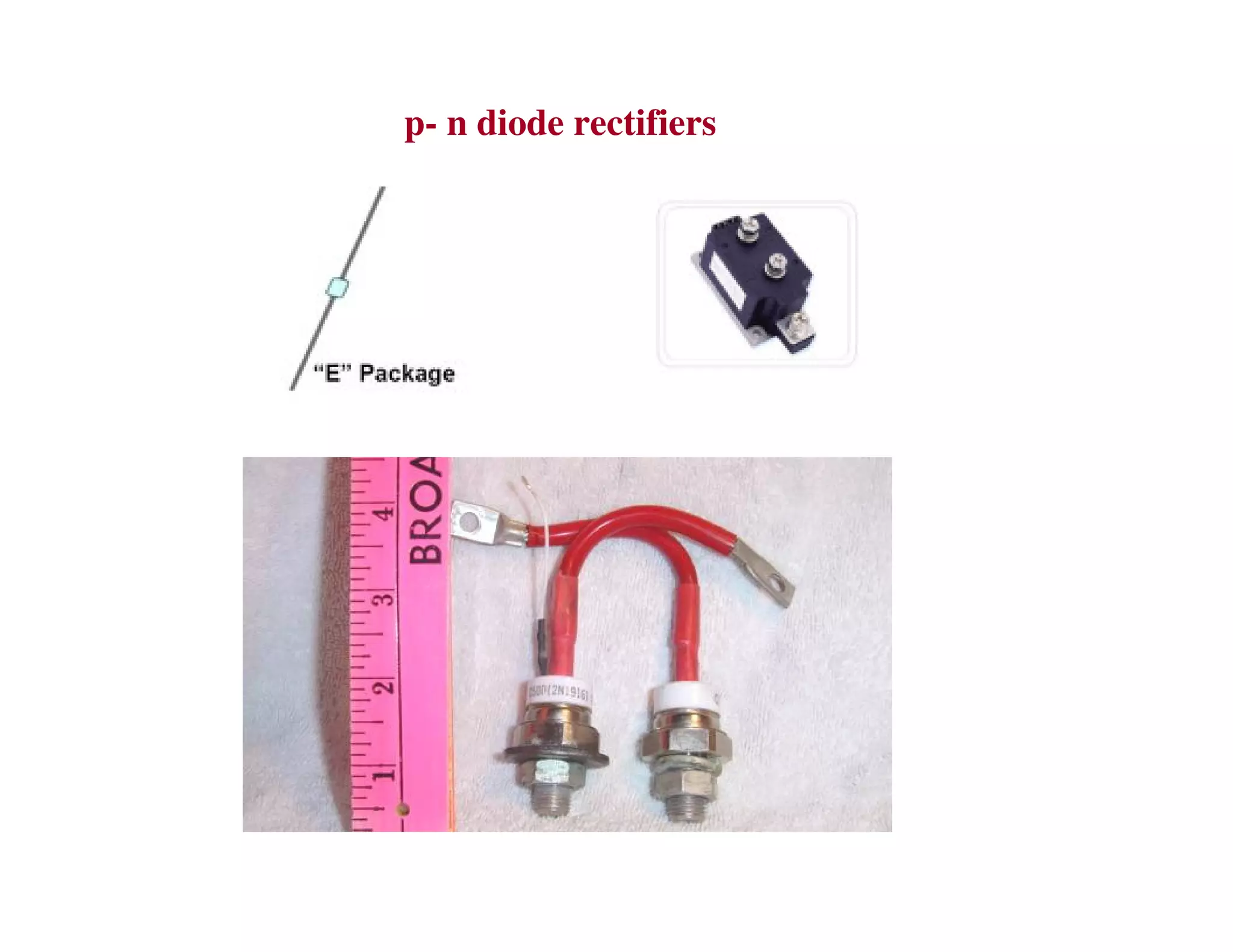
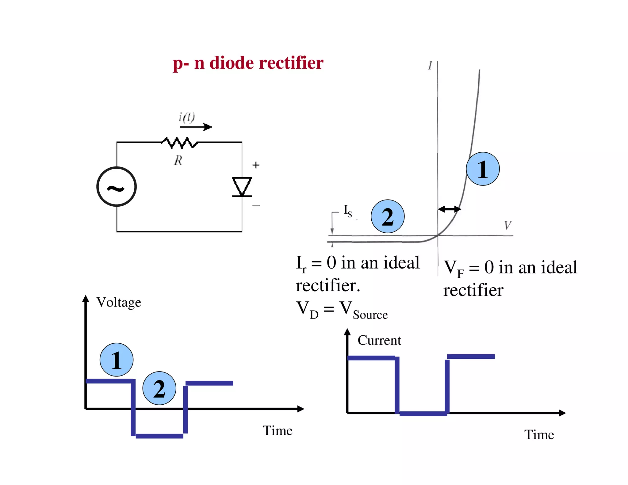
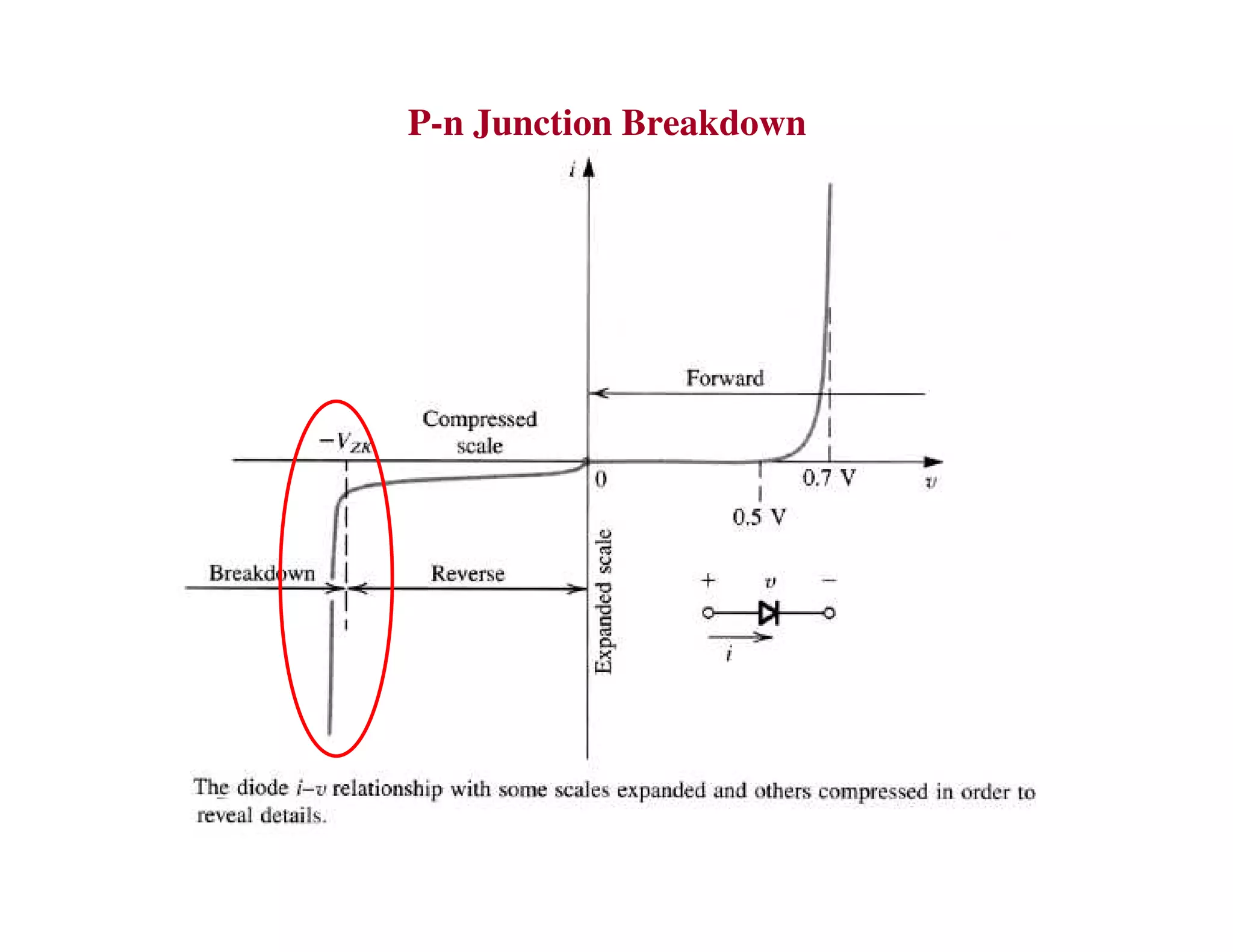
1. P-N diode rectifiers use the asymmetric conduction of P-N junctions to allow current in only one direction, rectifying an AC input into a pulsed DC output.
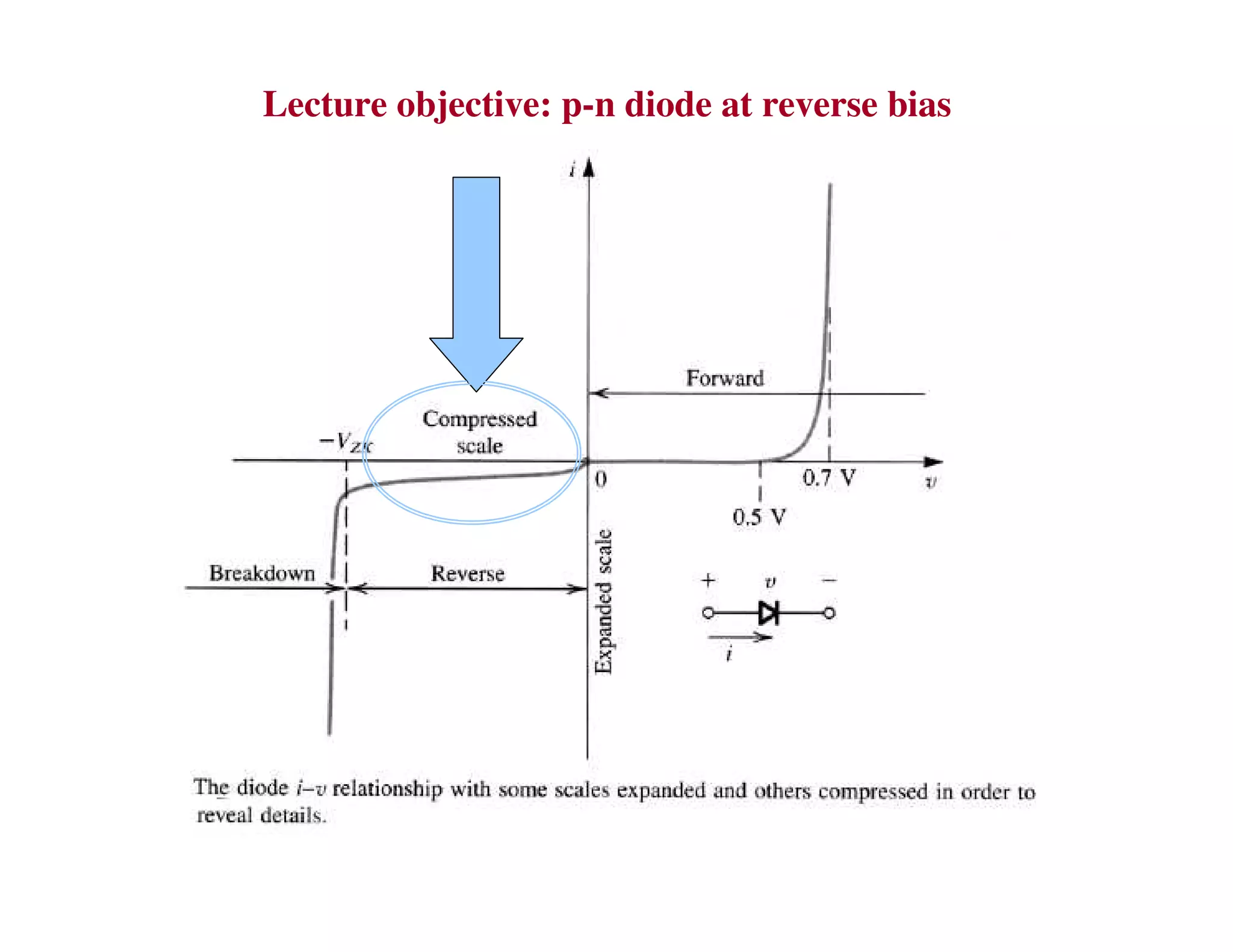
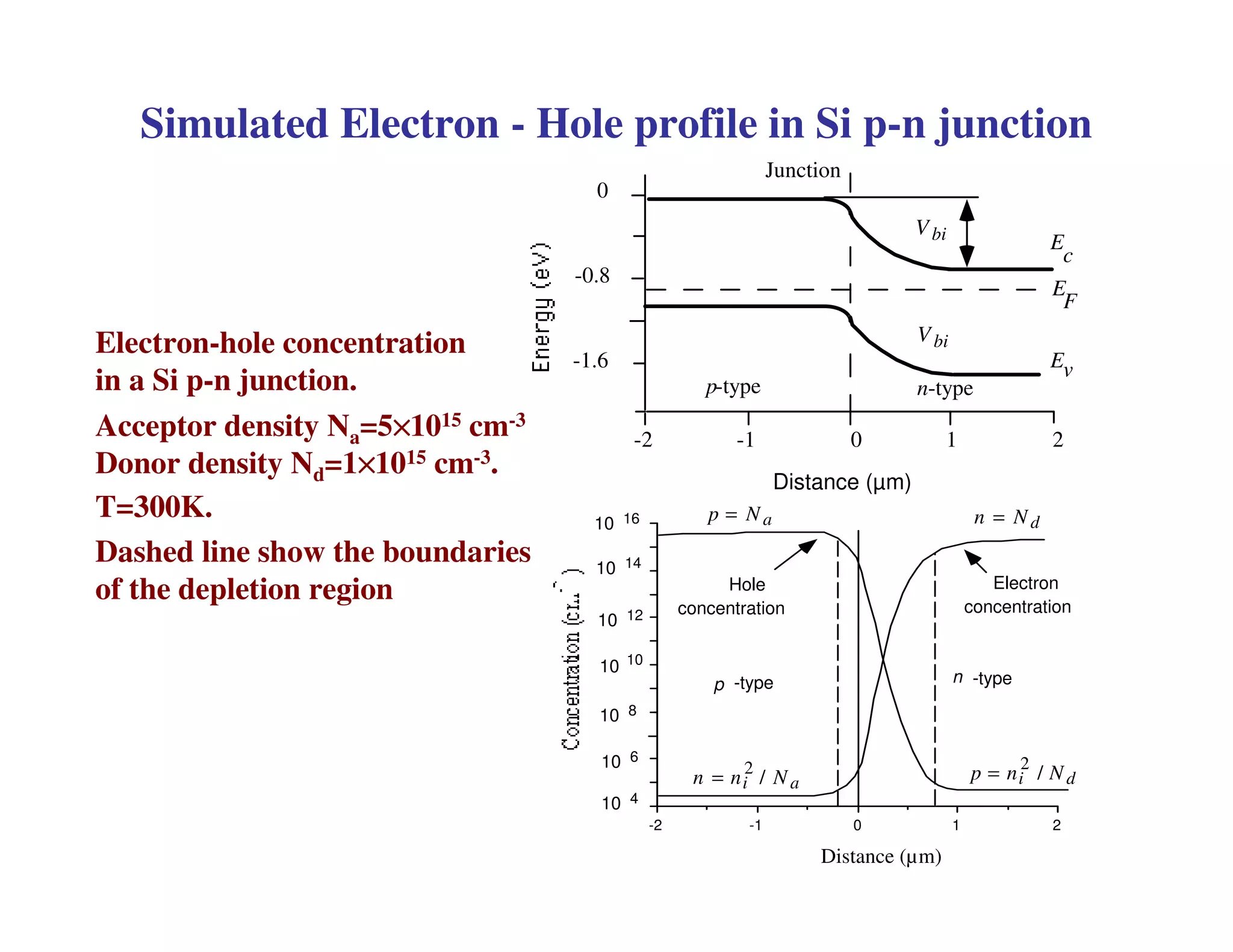
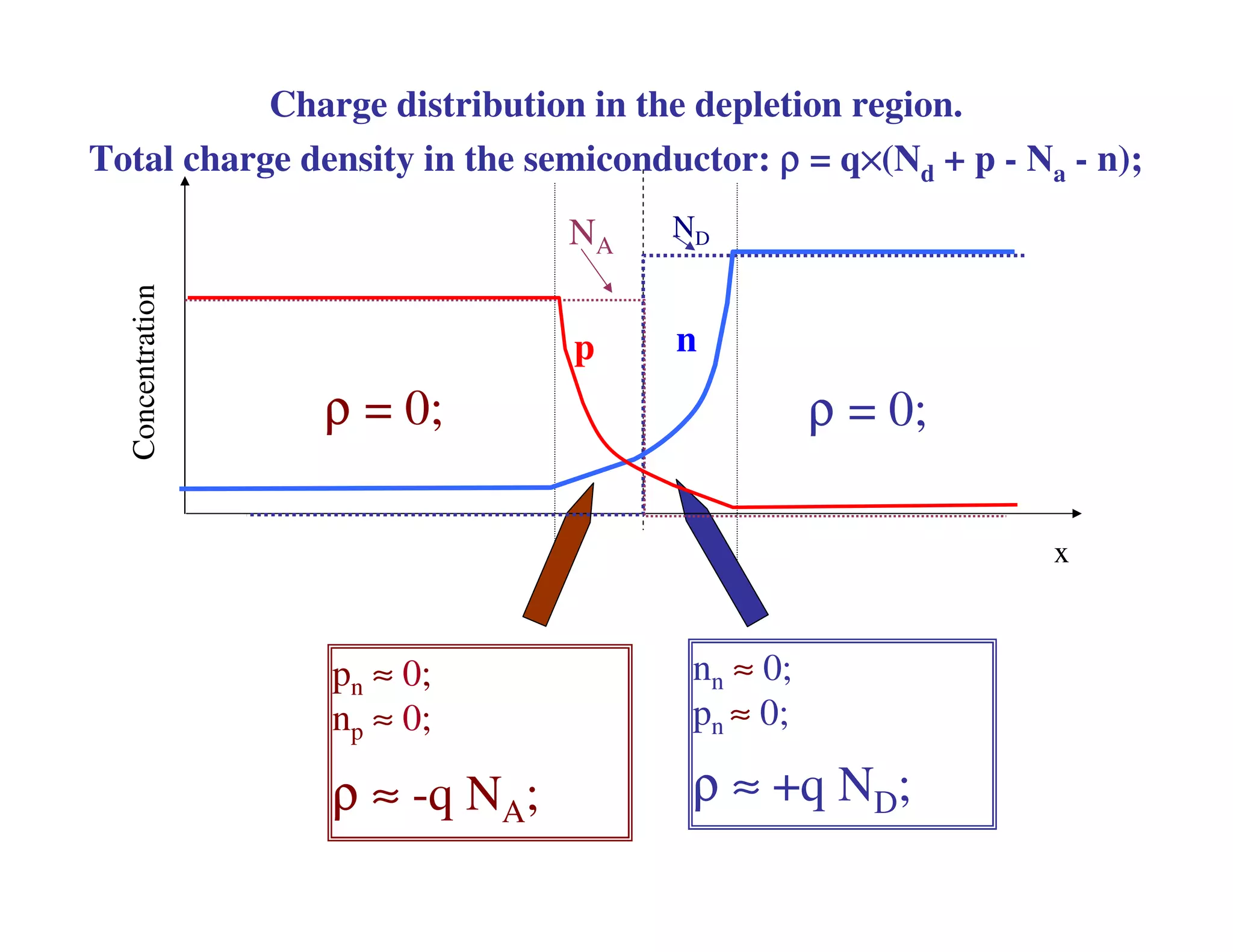
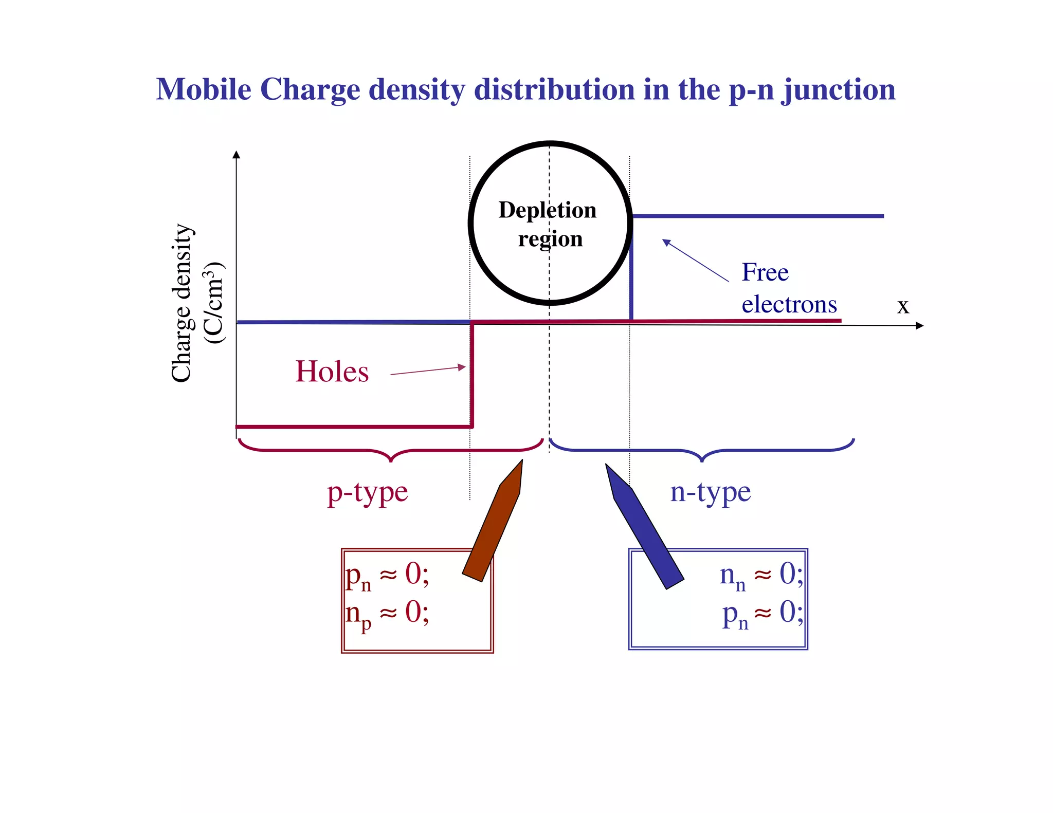
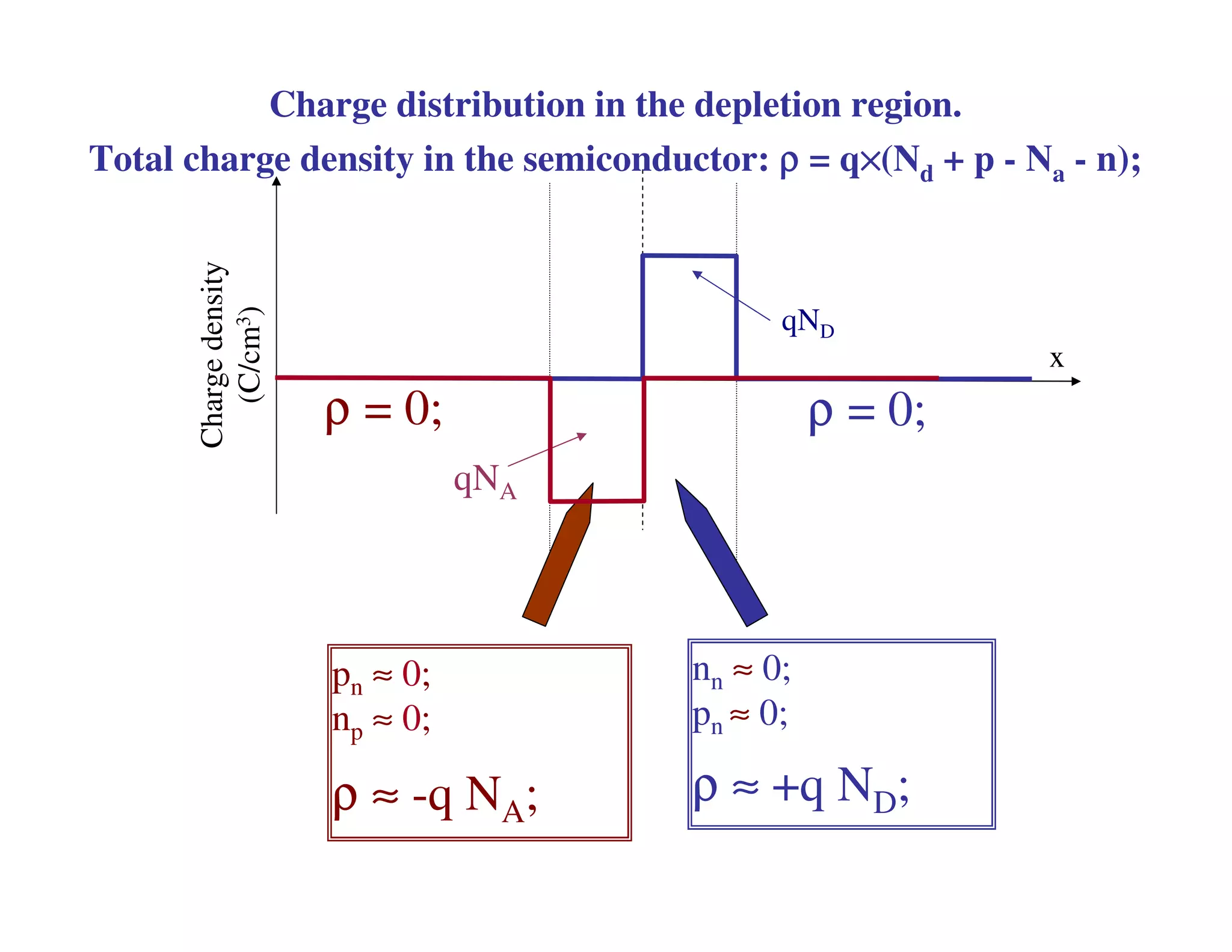
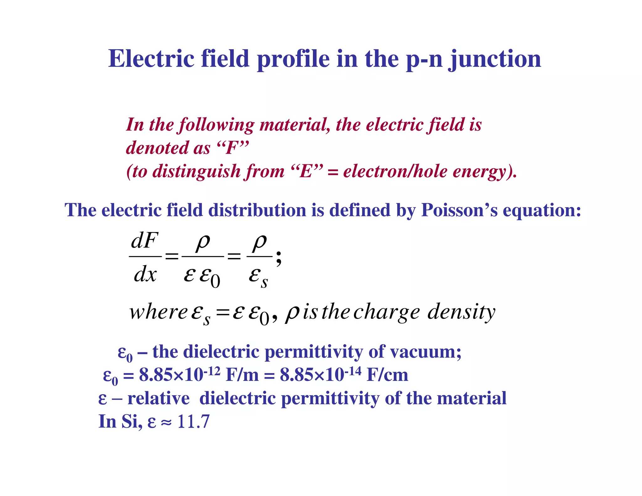
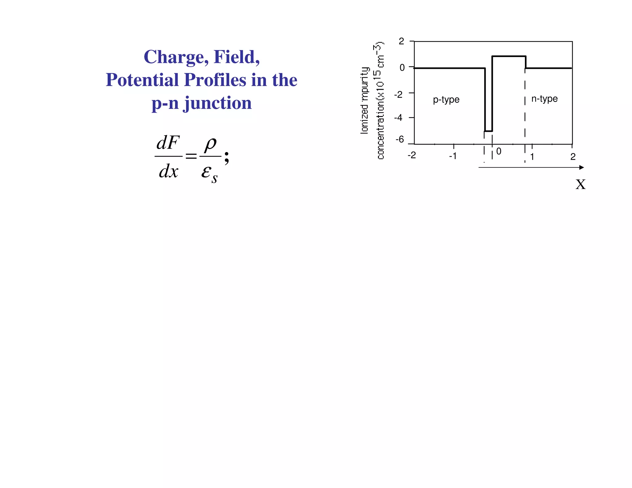
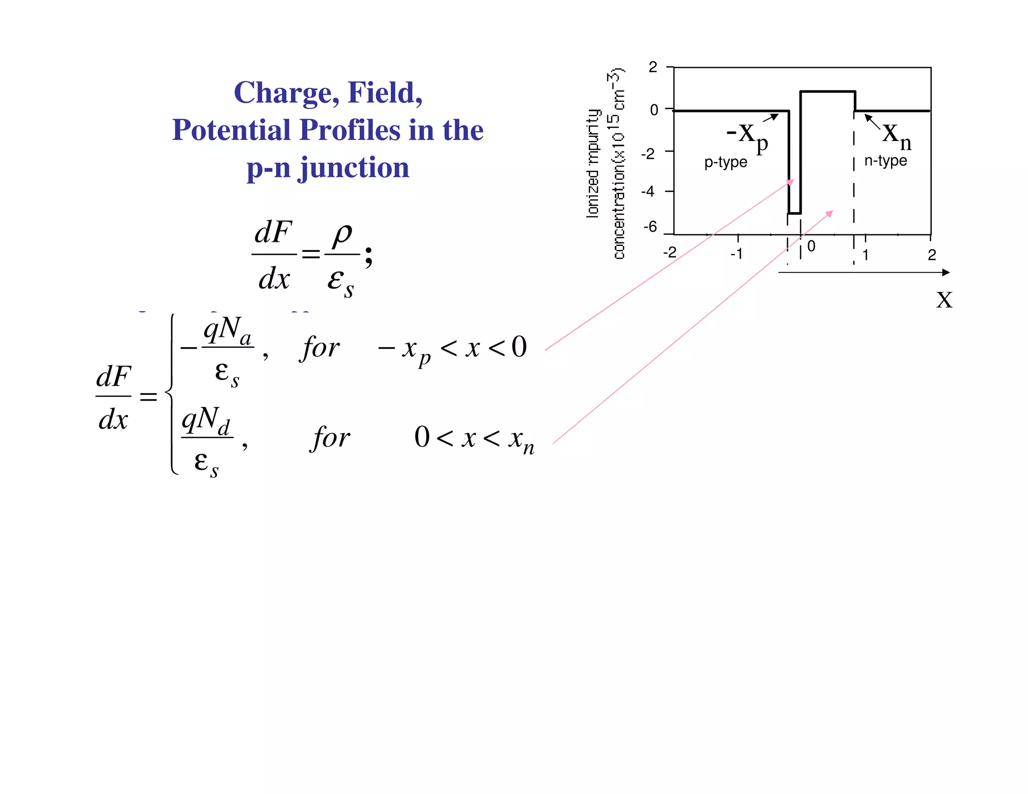
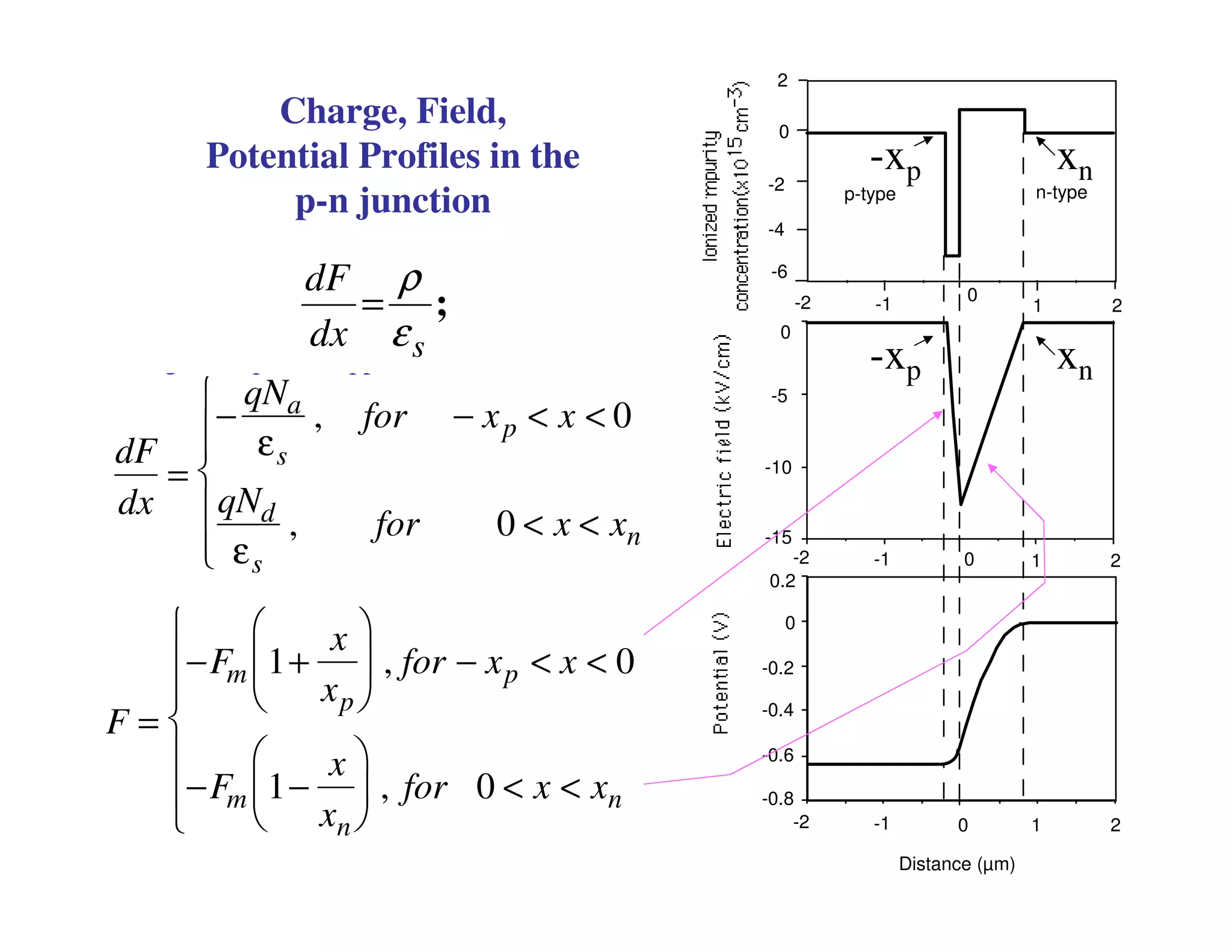
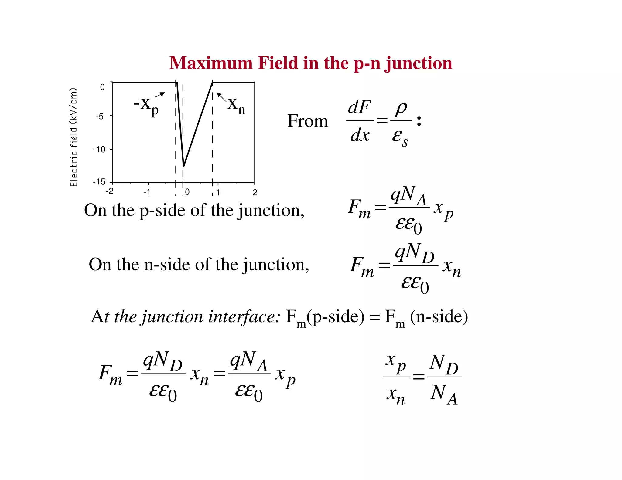
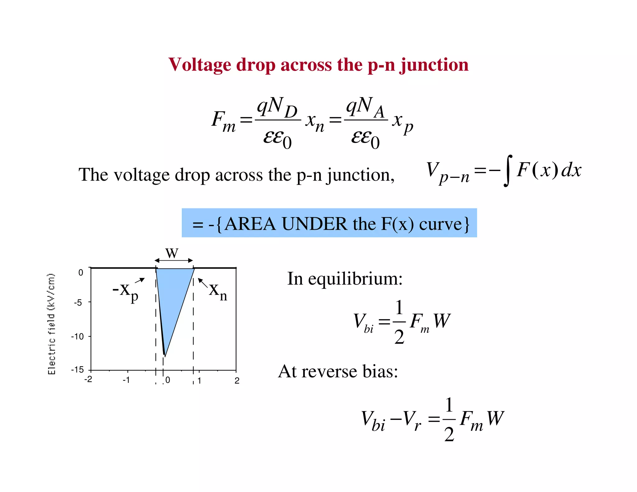
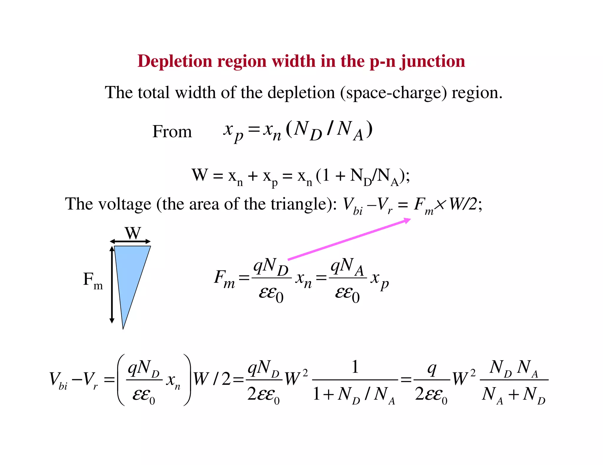
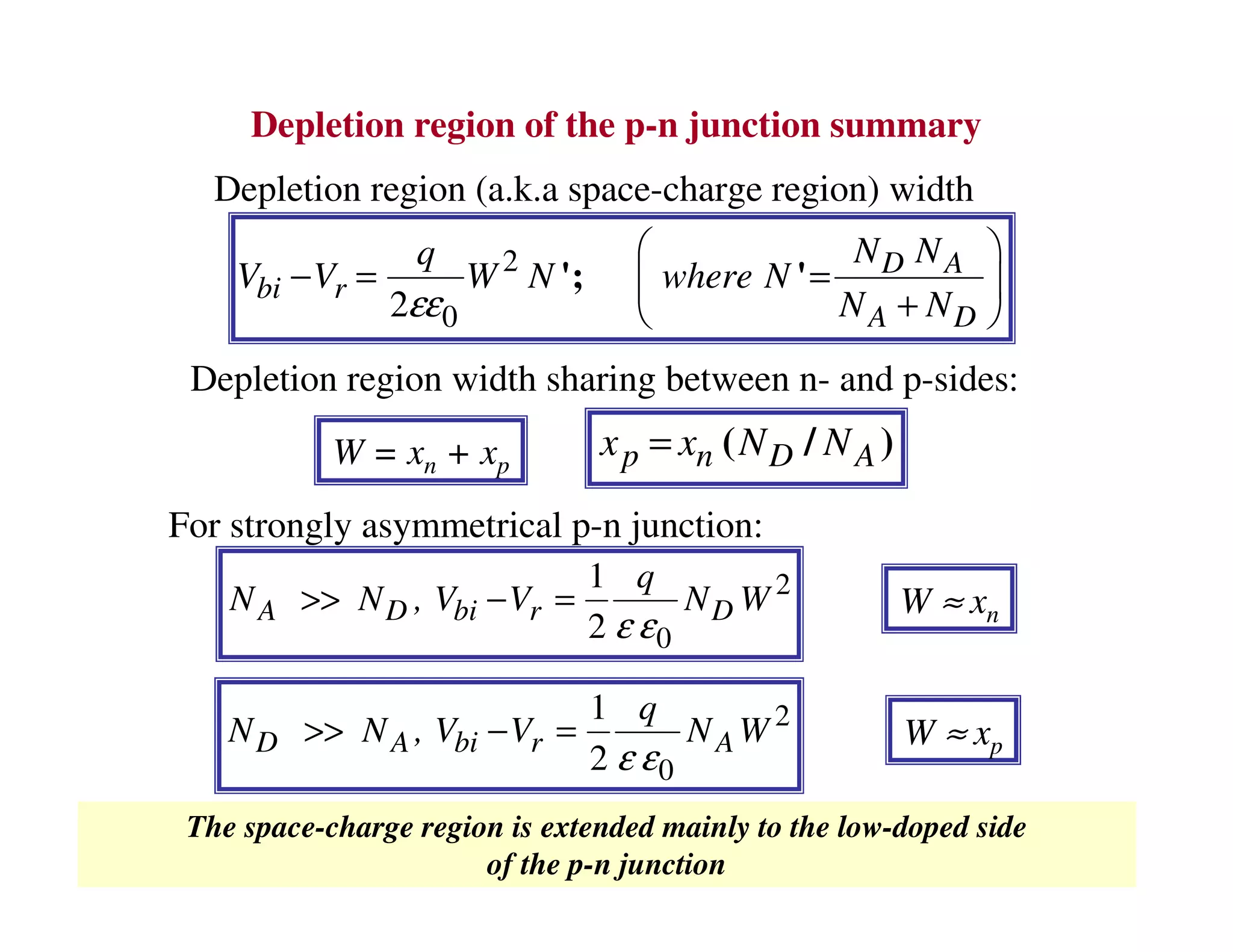
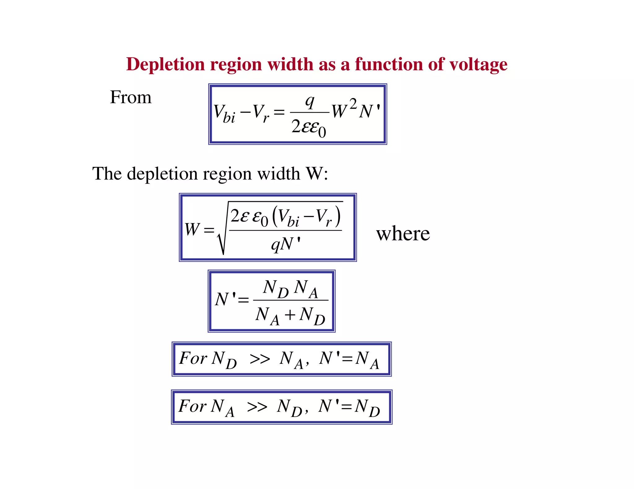
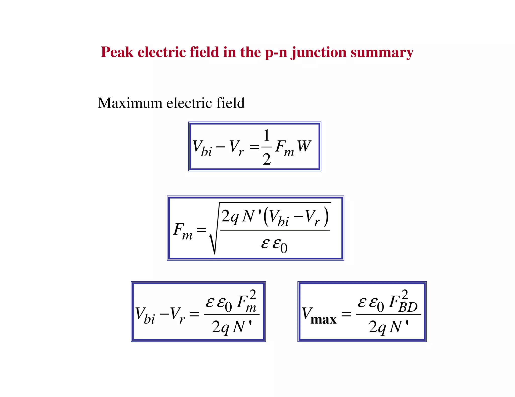
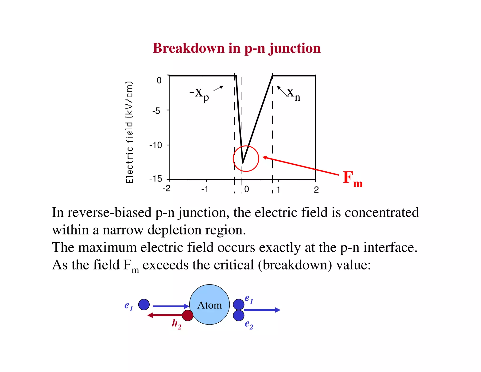
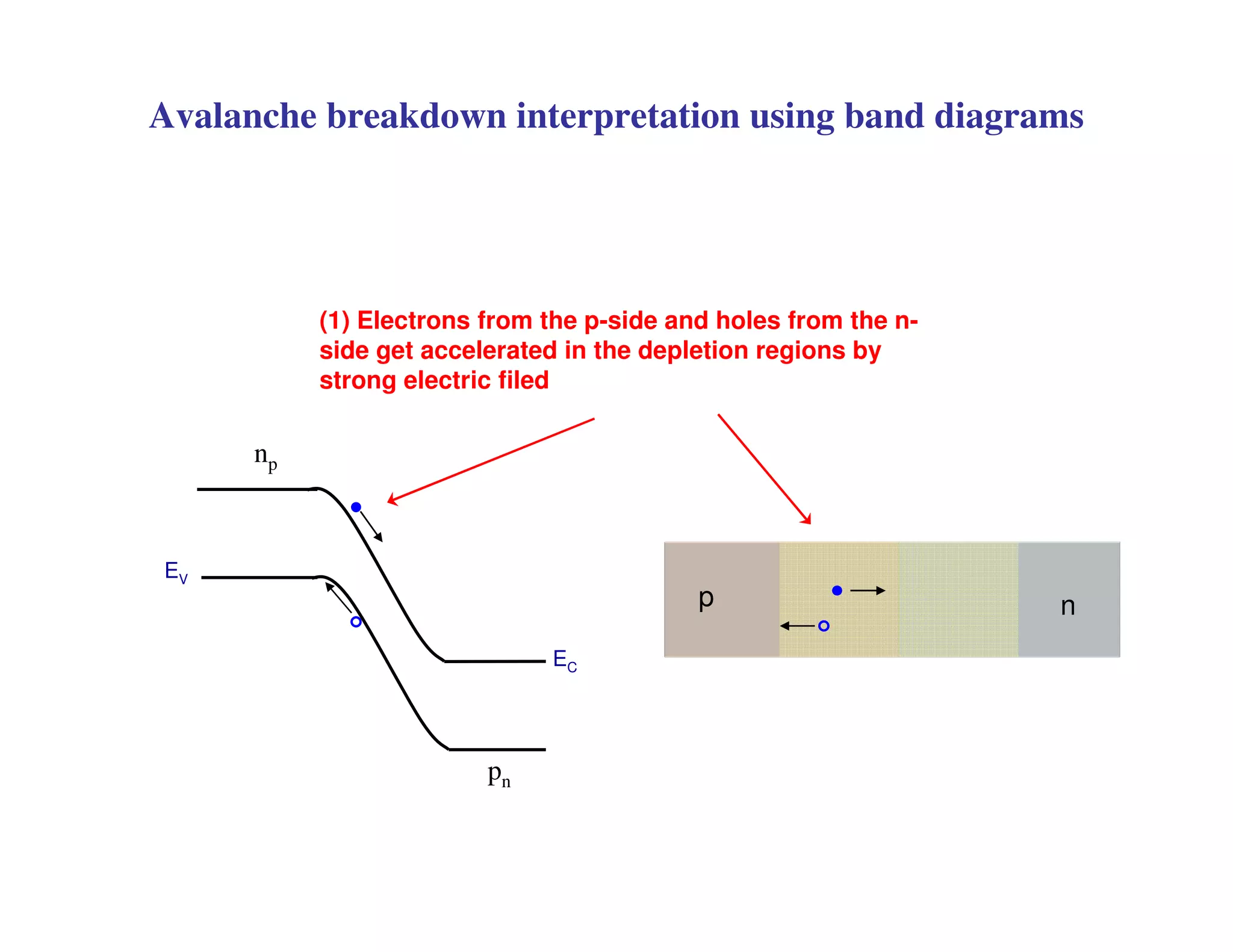
2. When a P-N junction is reverse biased, a depletion region forms where the P and N regions are depleted of mobile charge carriers. This results in a built-in electric field.
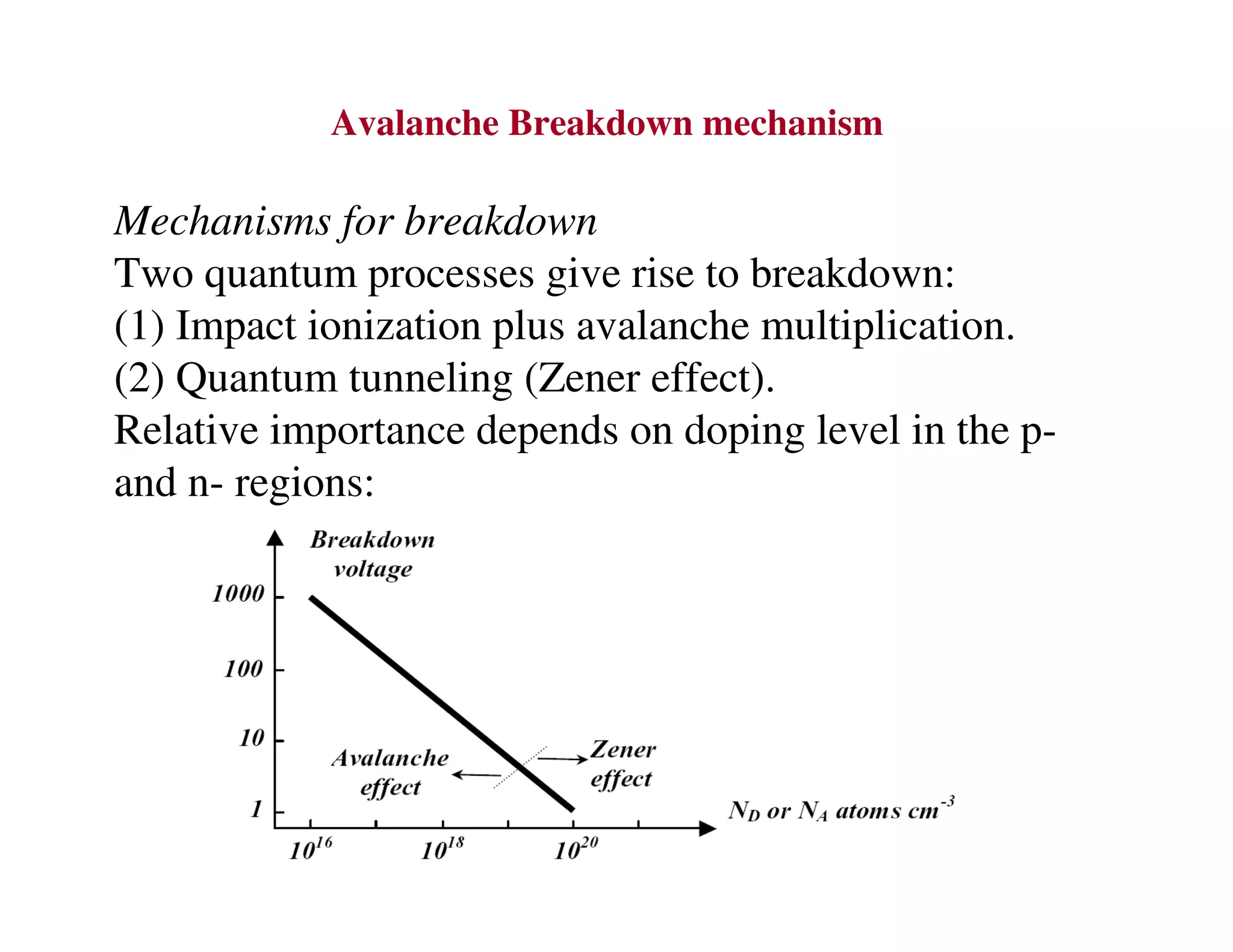
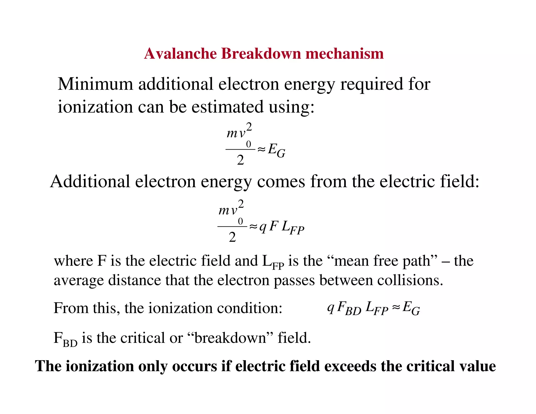
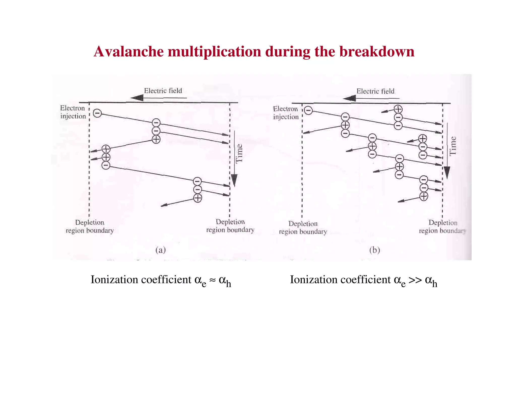
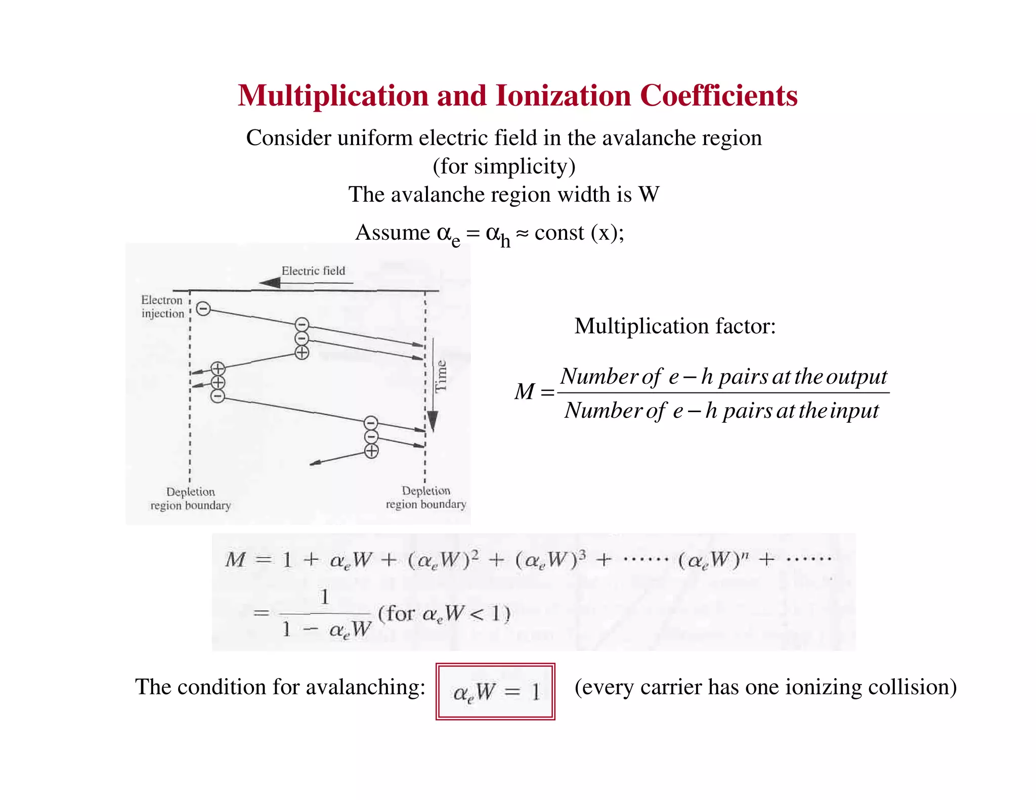
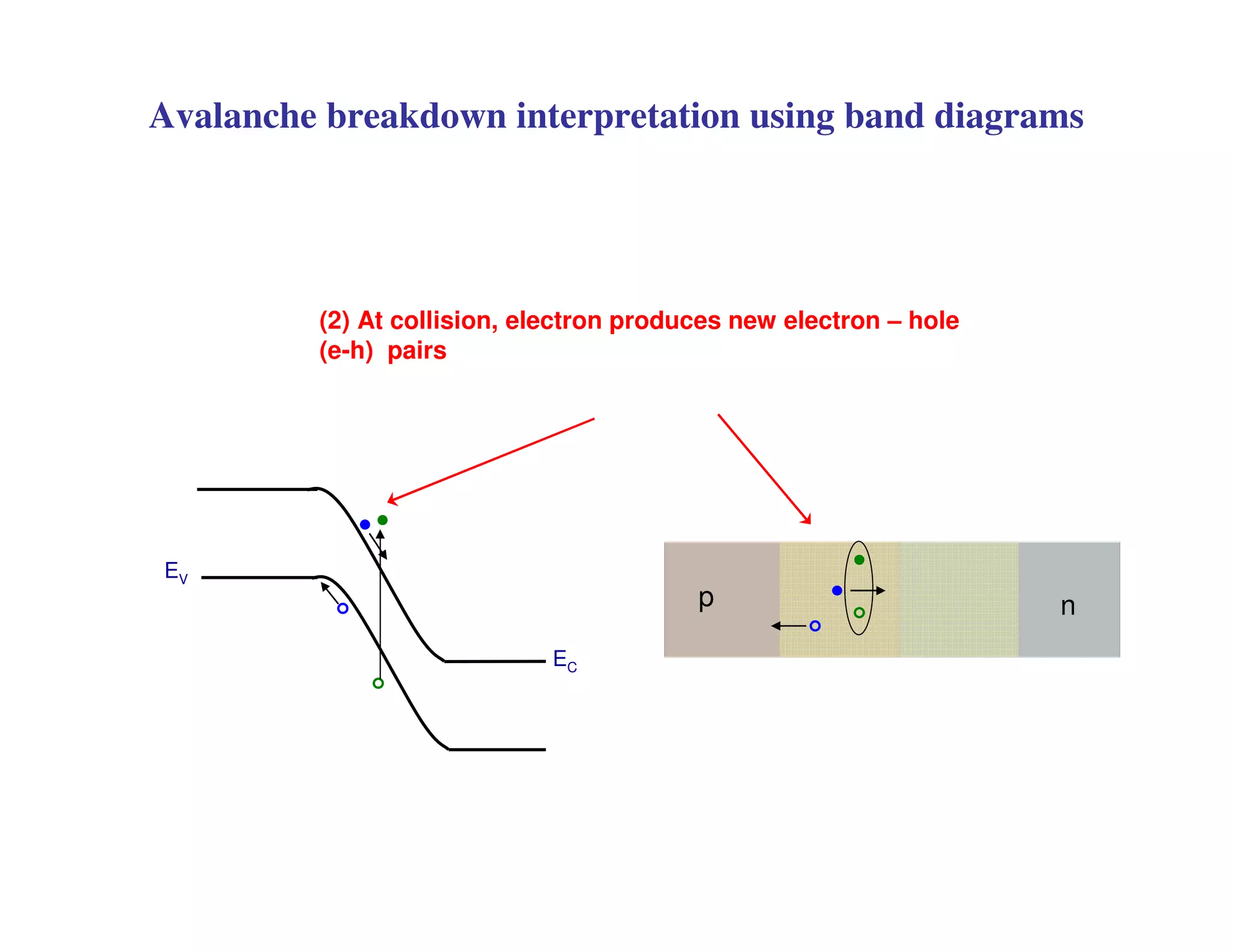
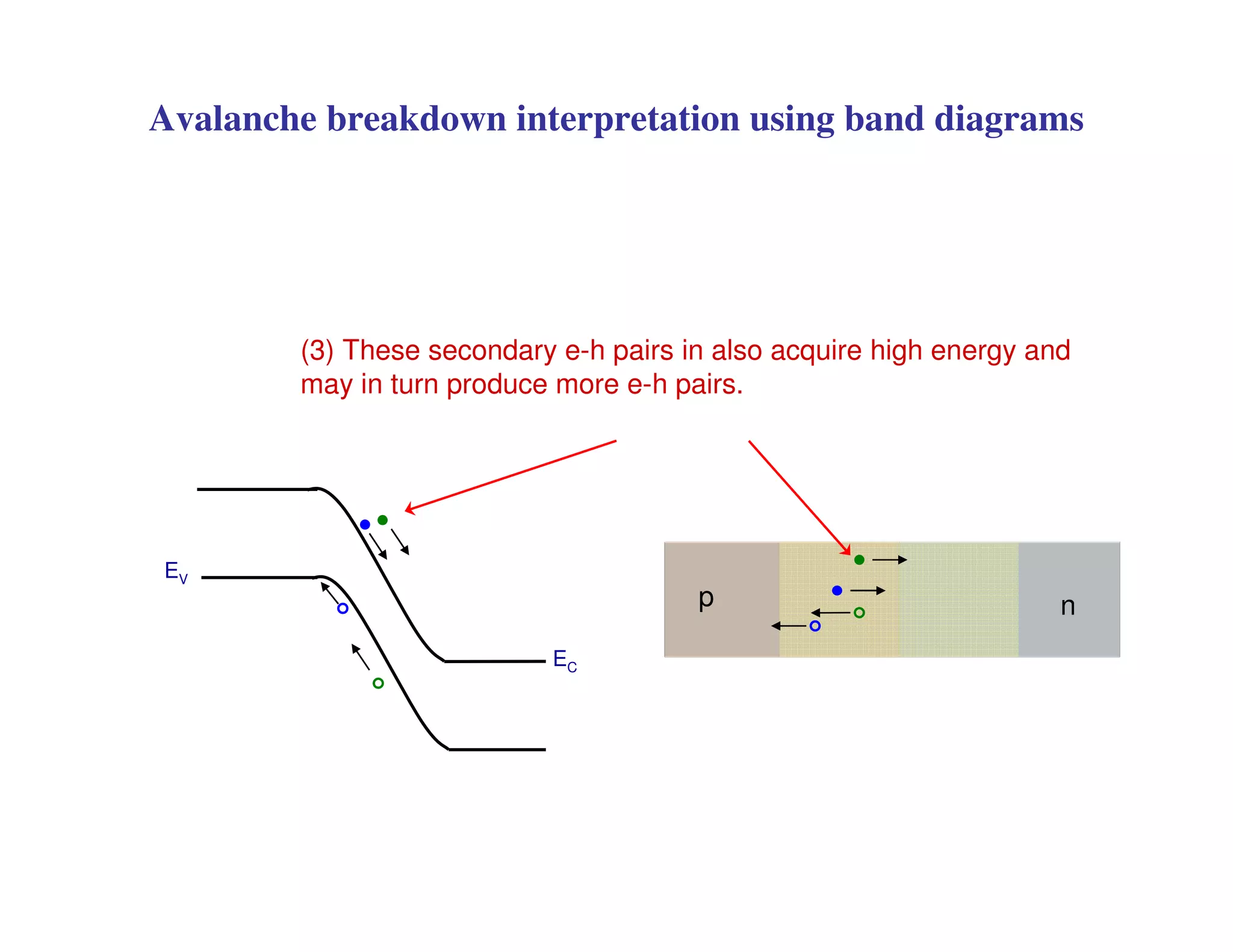
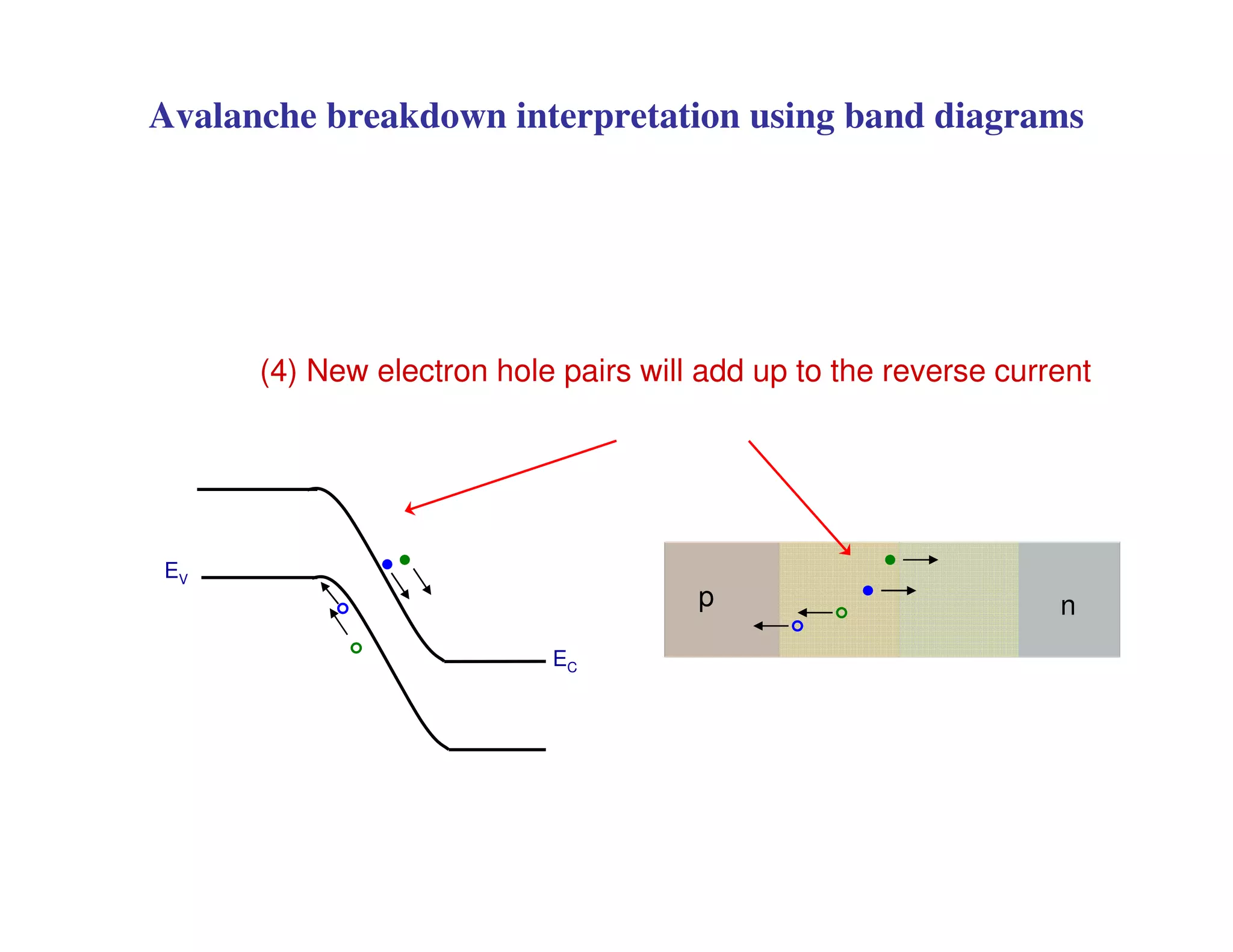
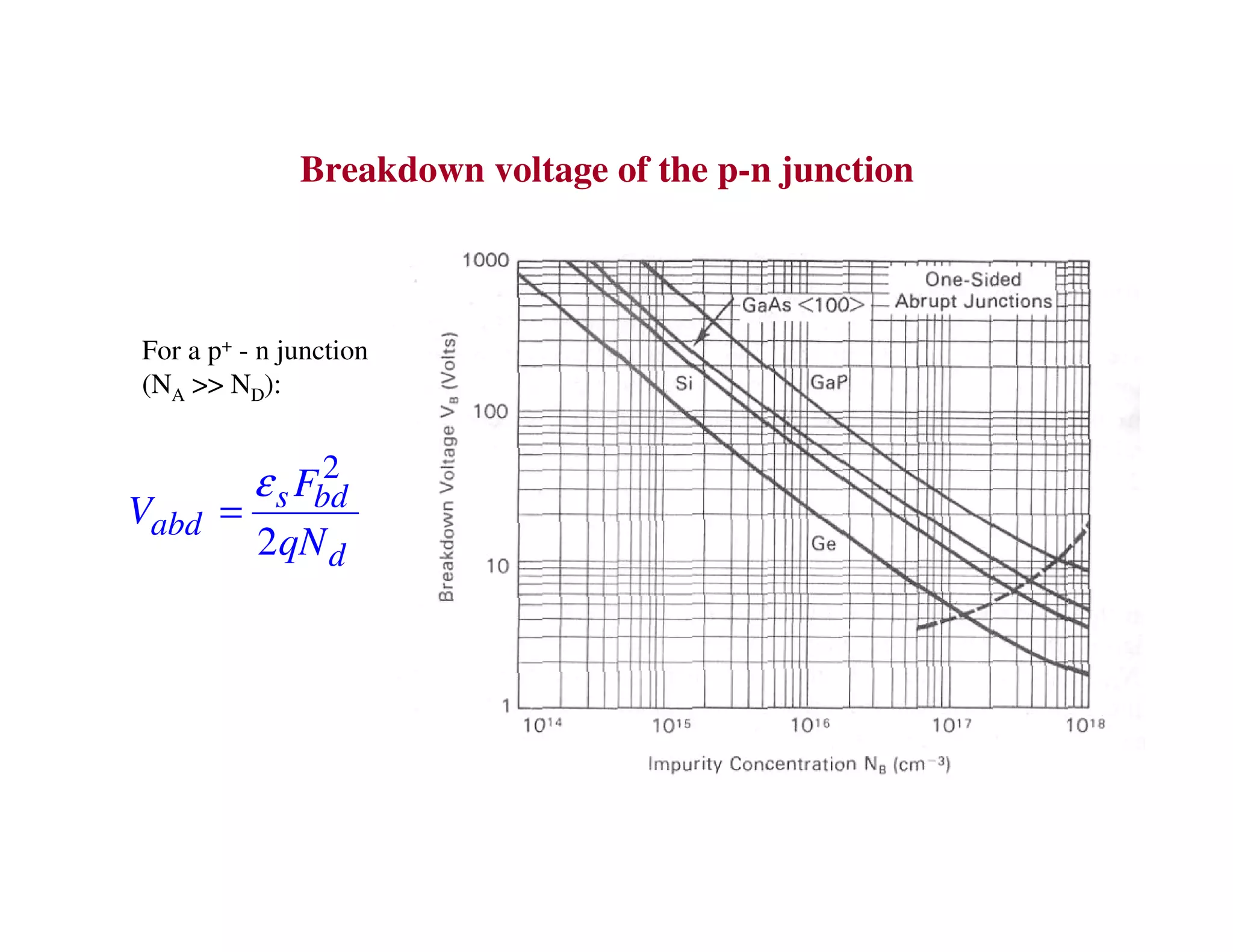
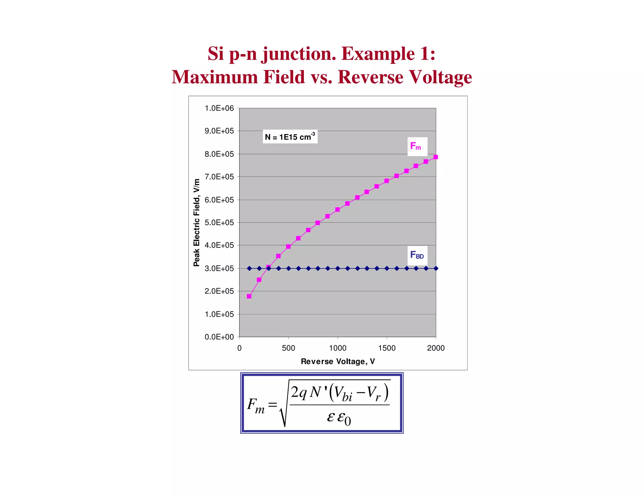
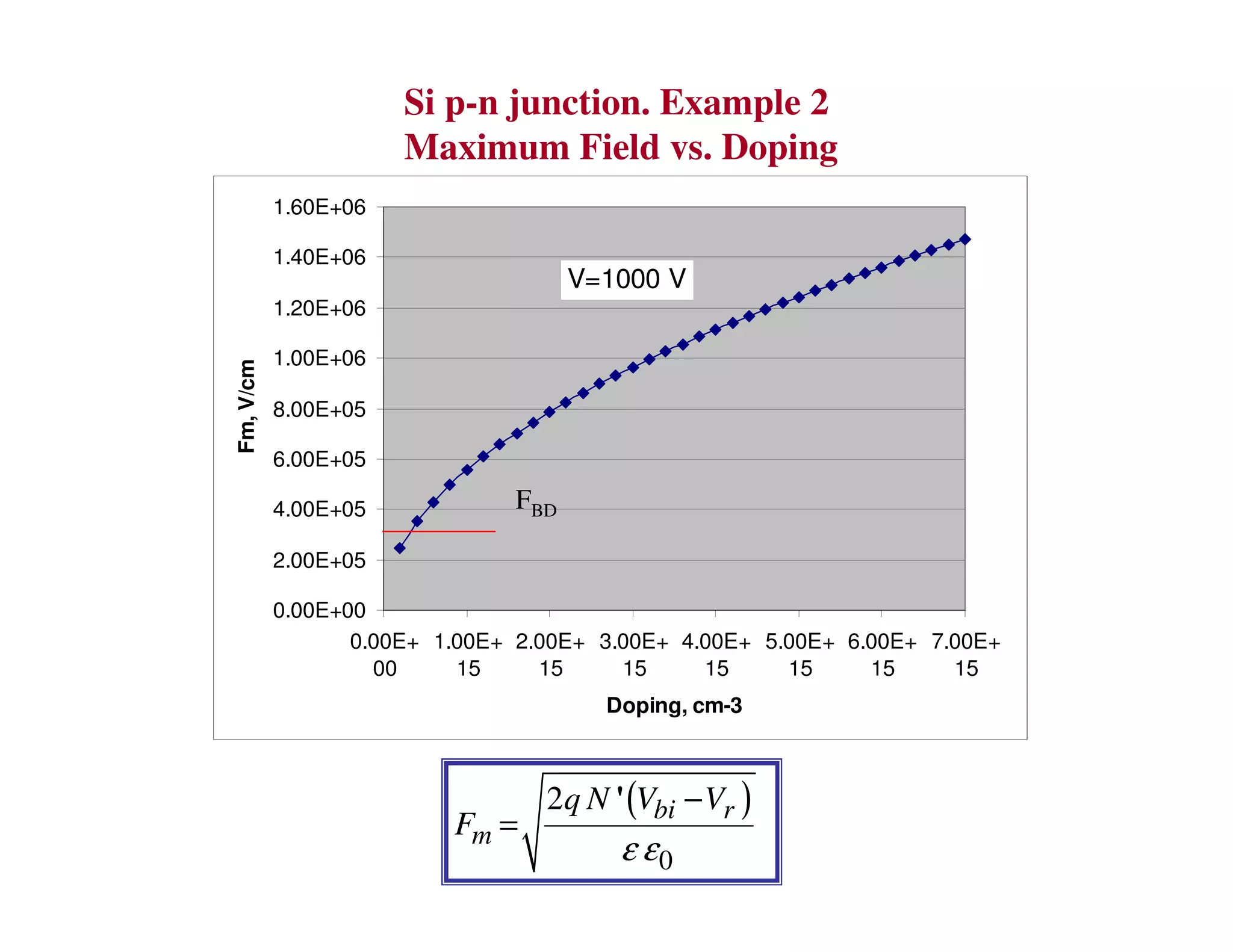
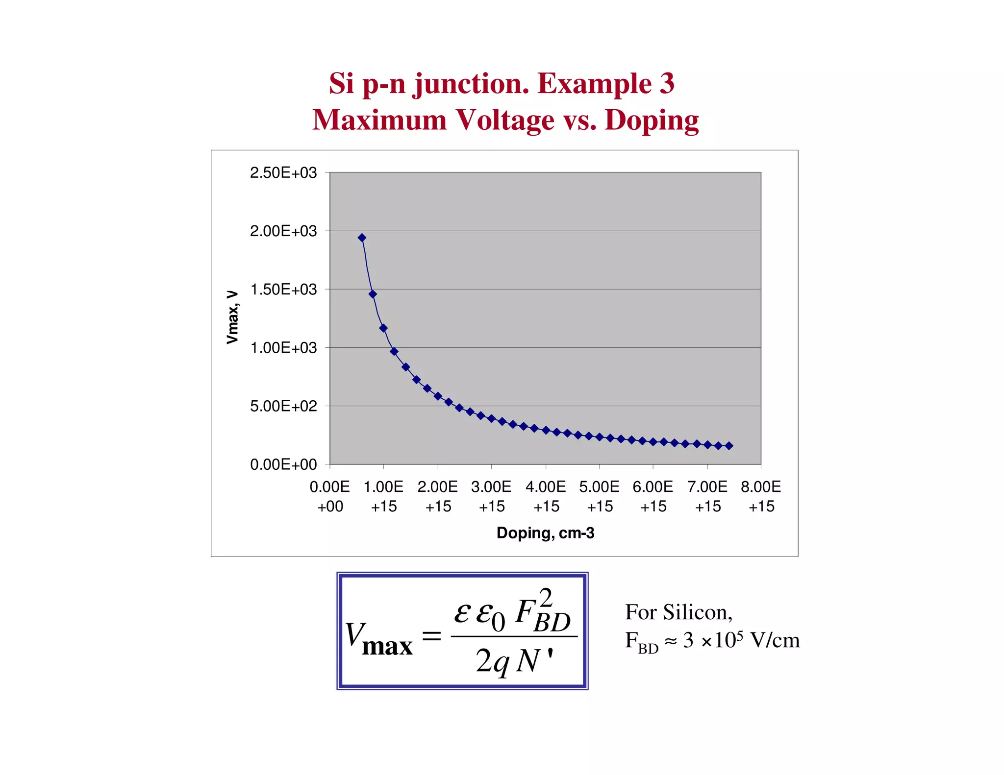
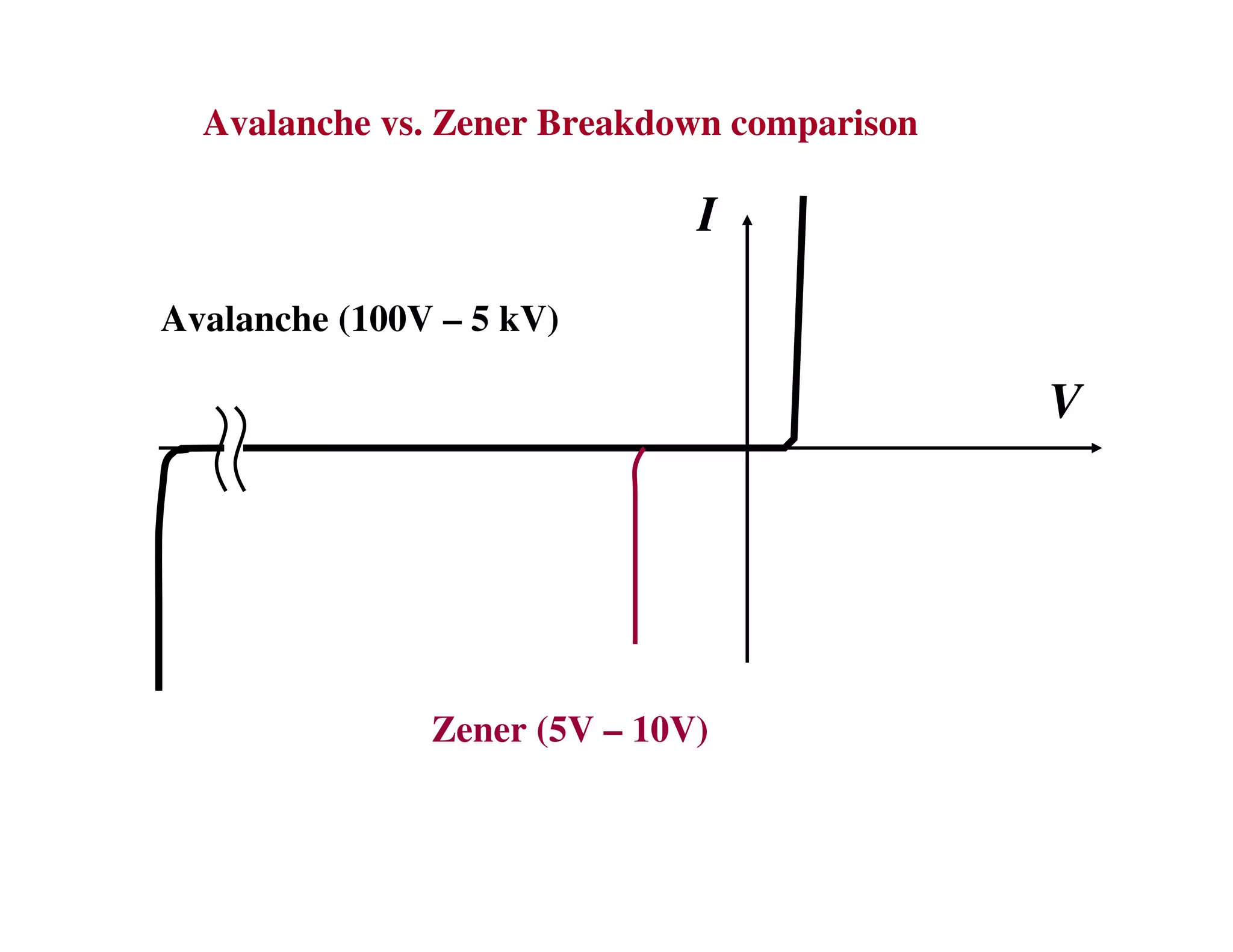
3. Under sufficient reverse bias, avalanche breakdown can occur where the built-in electric field accelerates carriers to energies high enough to liberate other carriers through impact ionization, causing an avalanche multiplication of carriers and a sharp rise in reverse current.