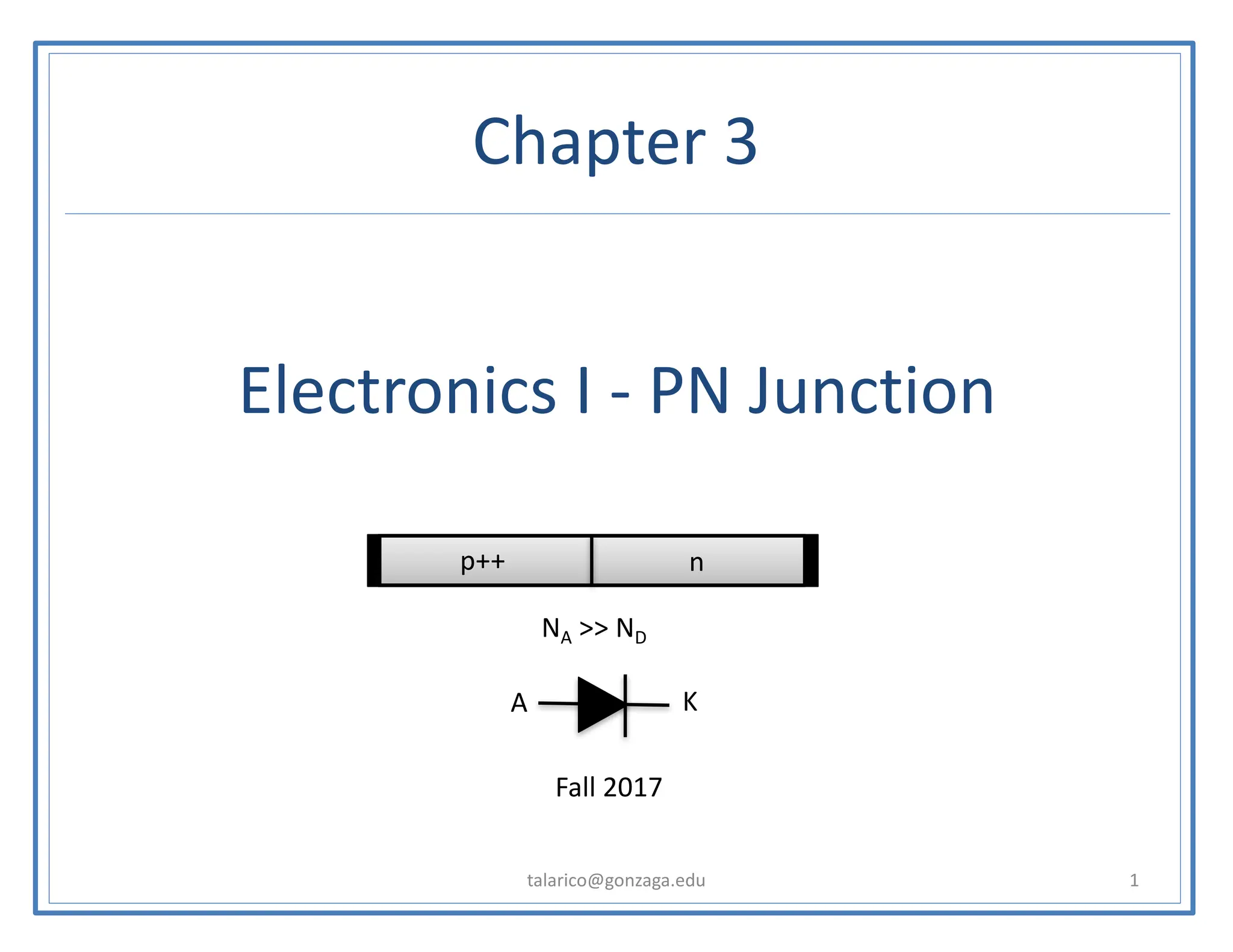
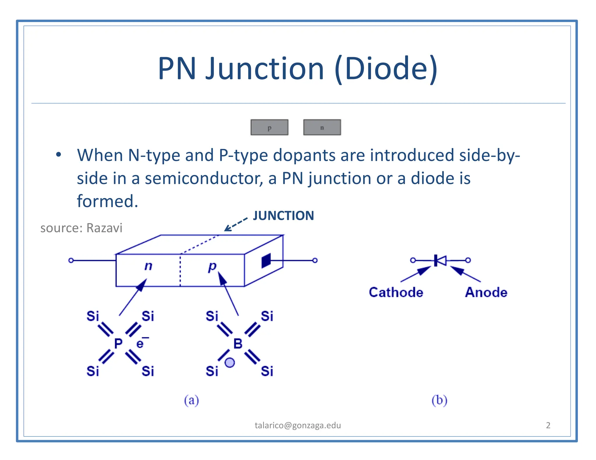
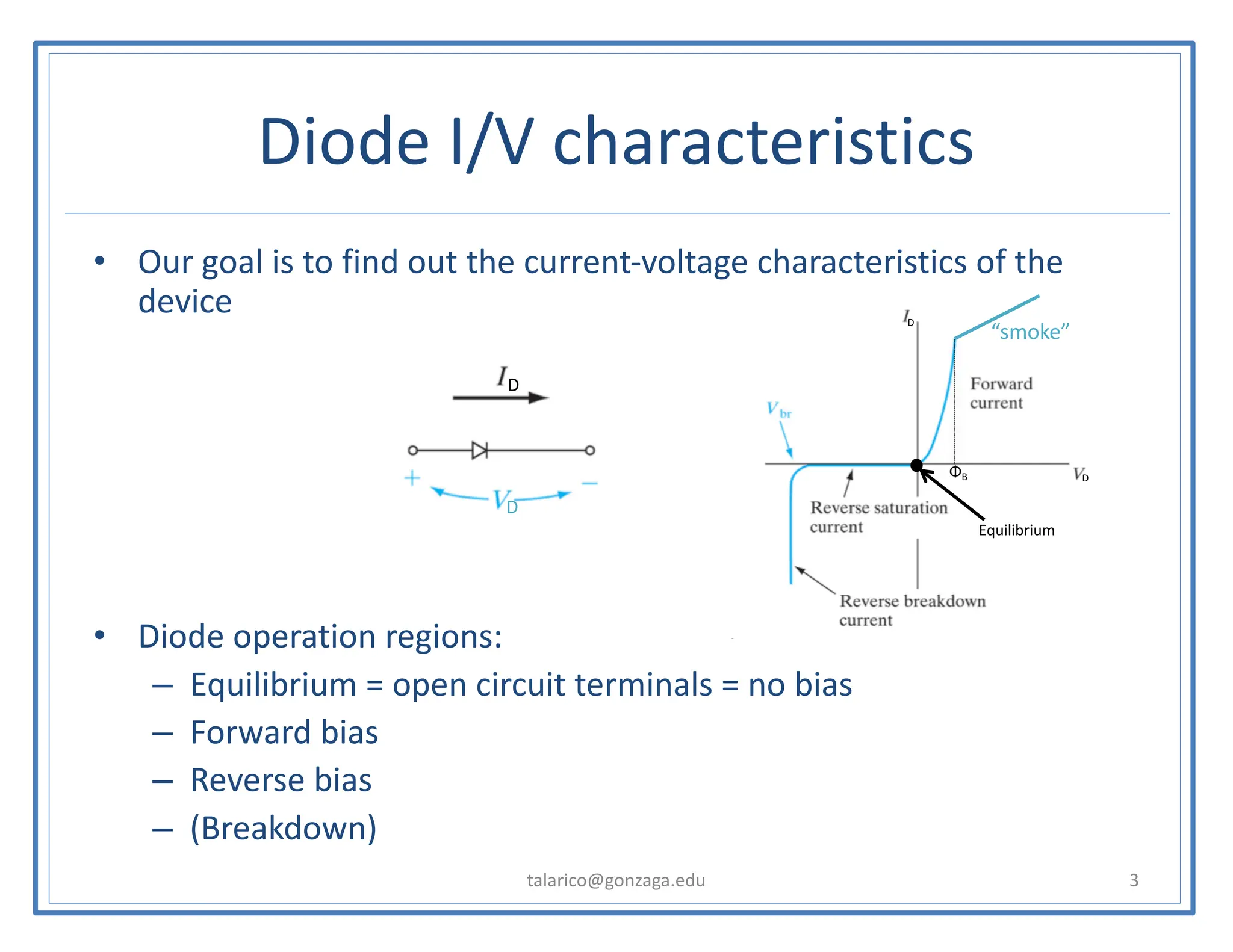
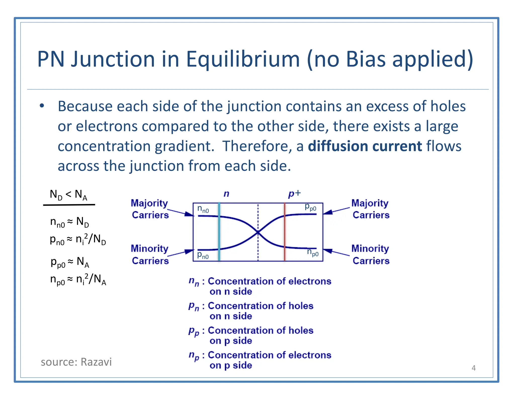
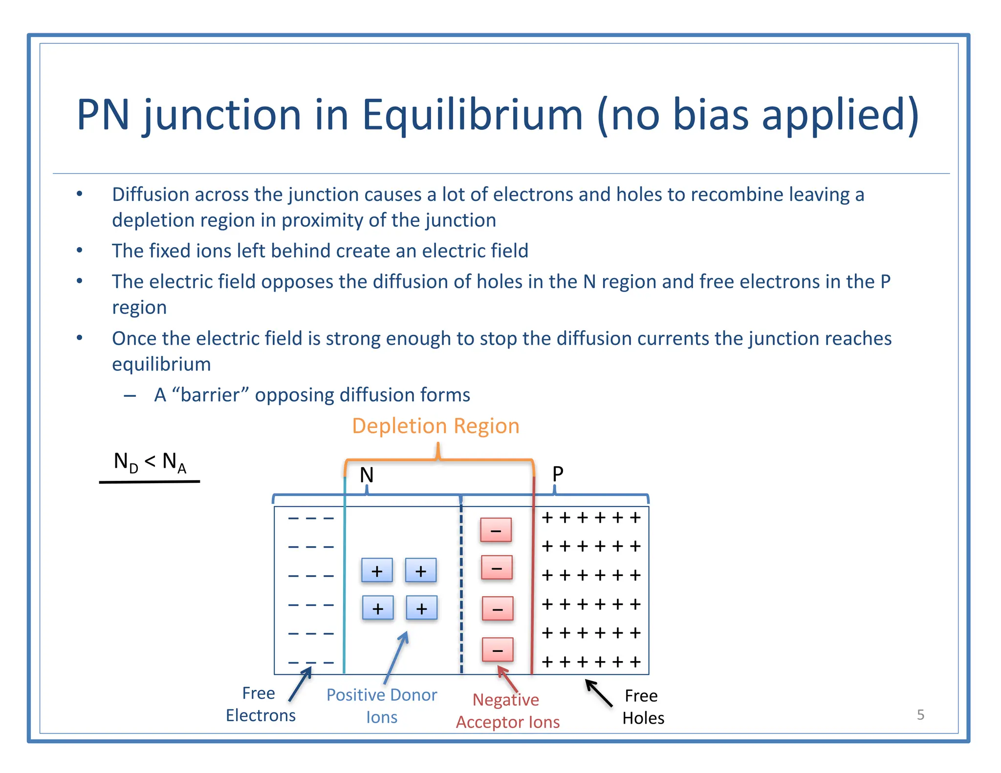
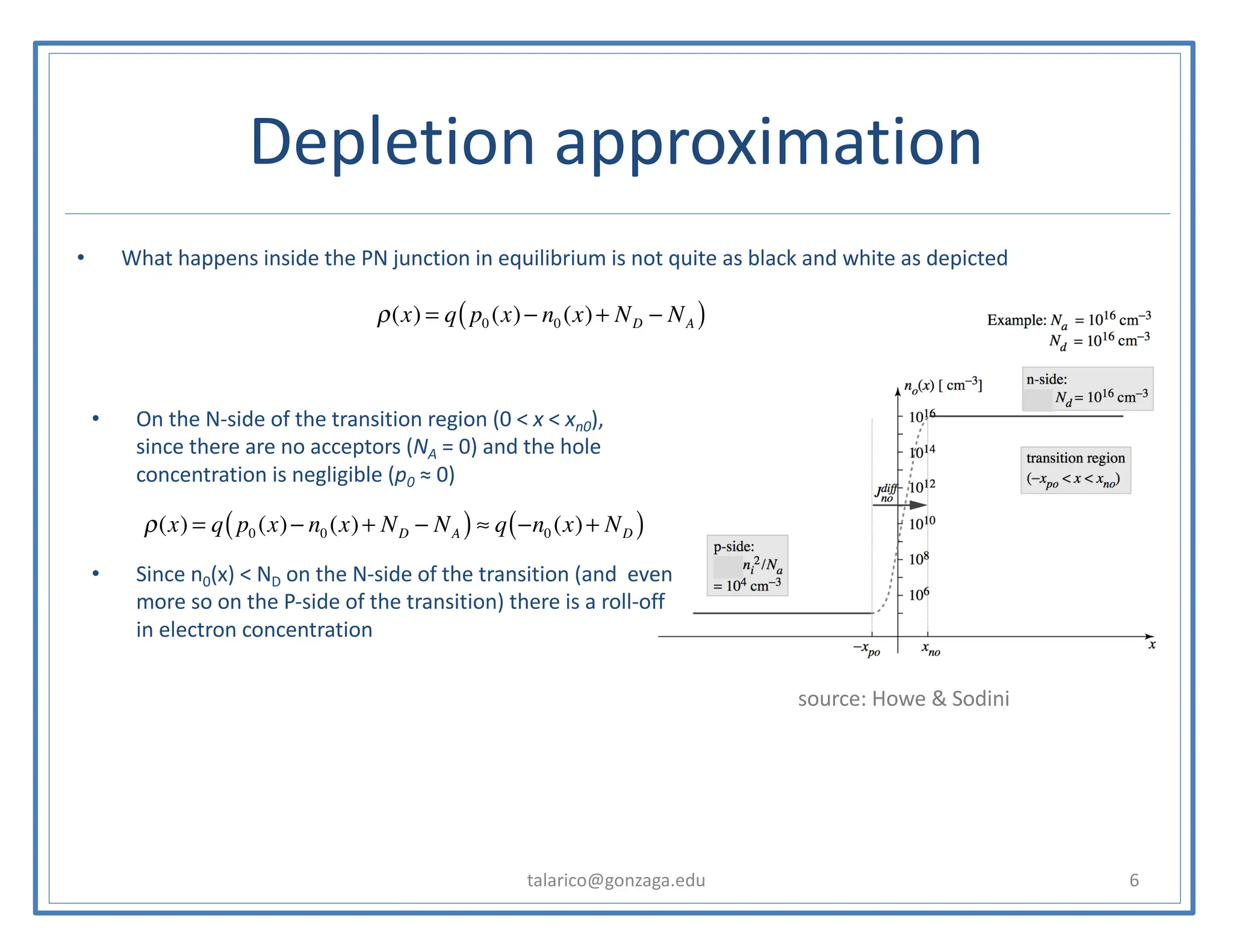
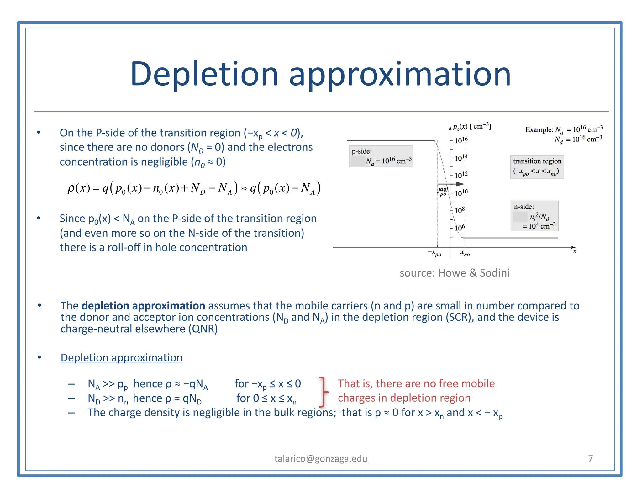
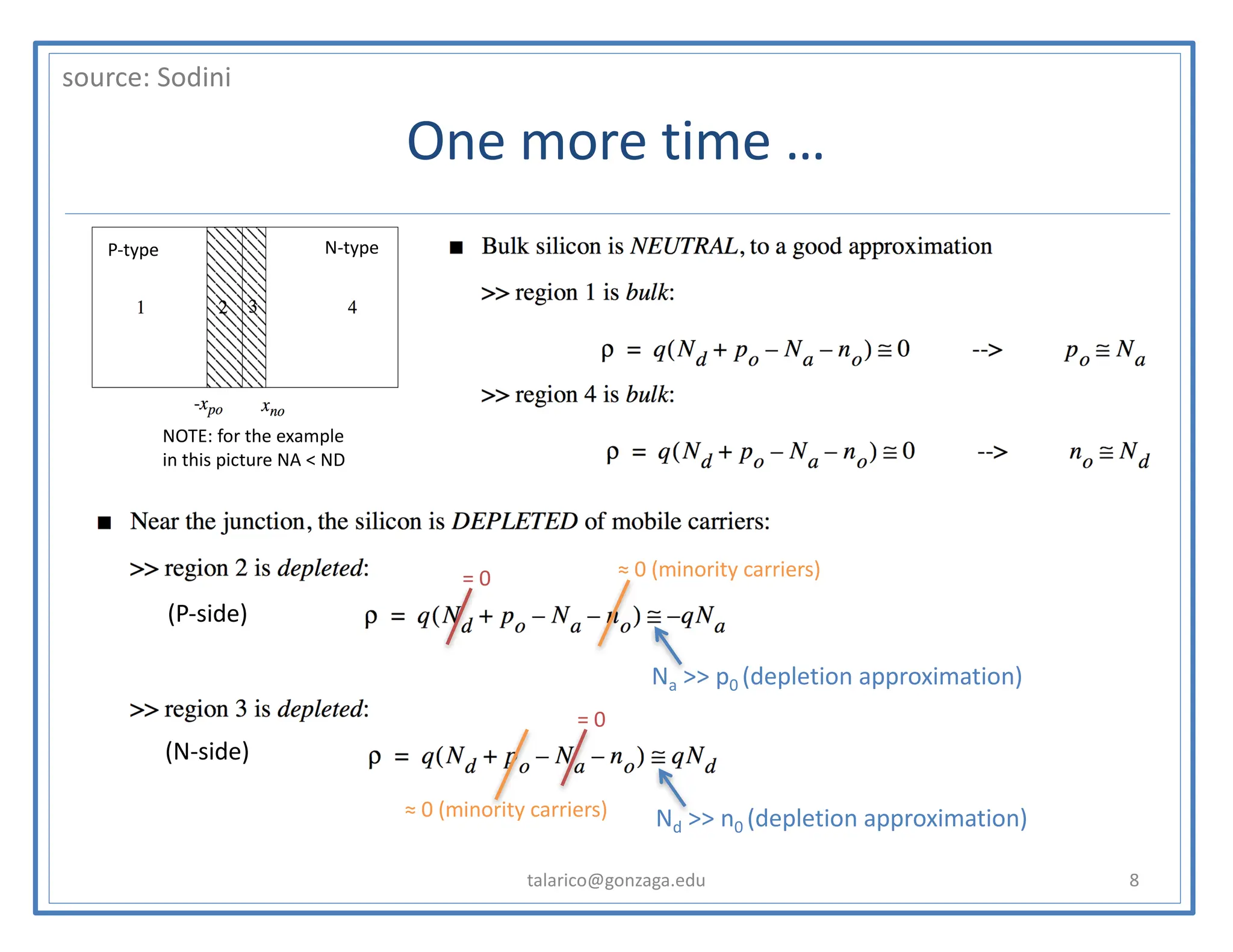
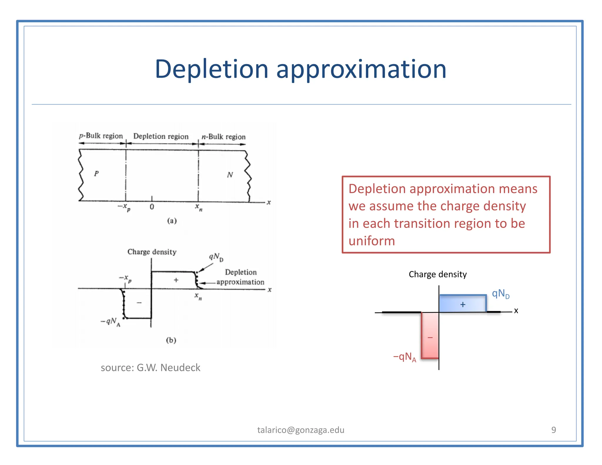
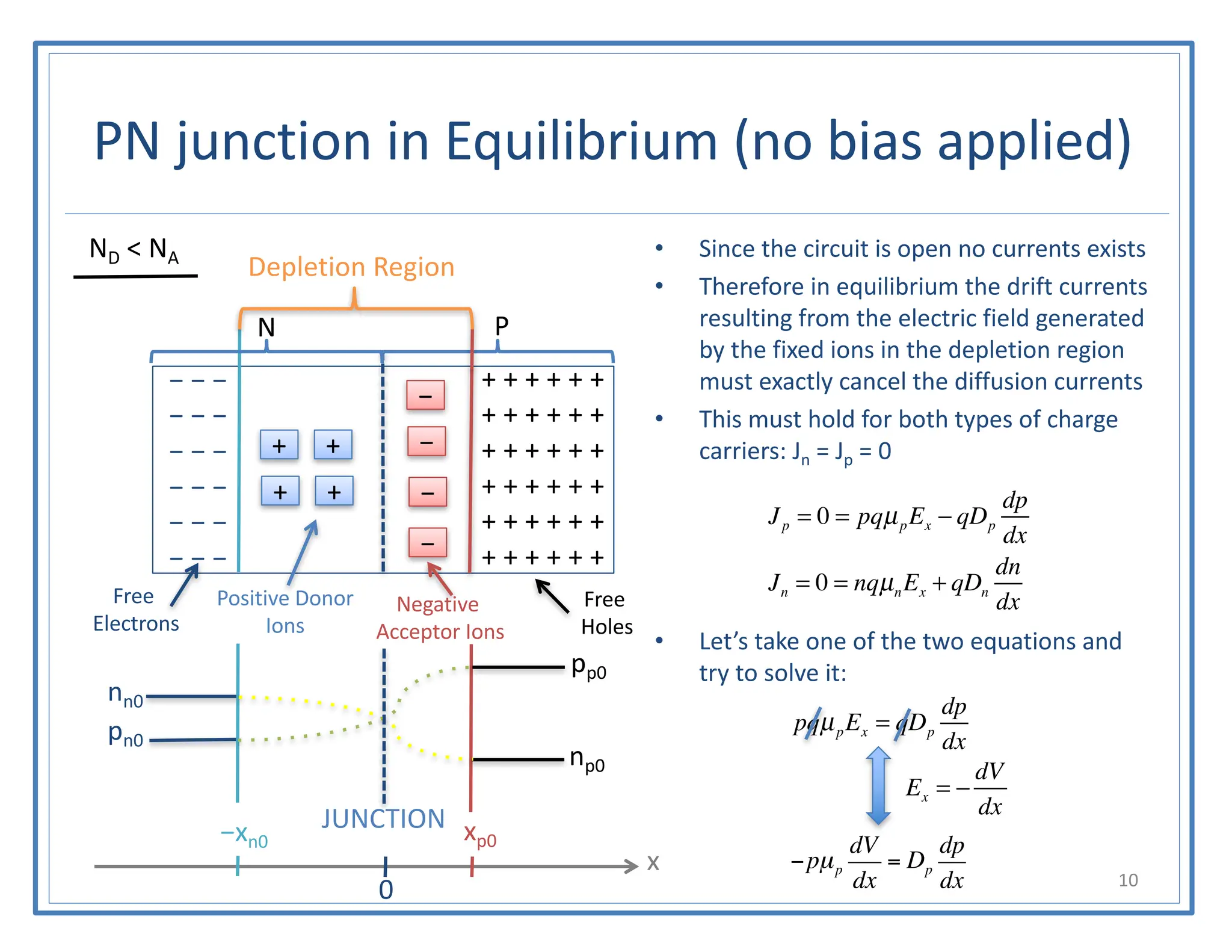
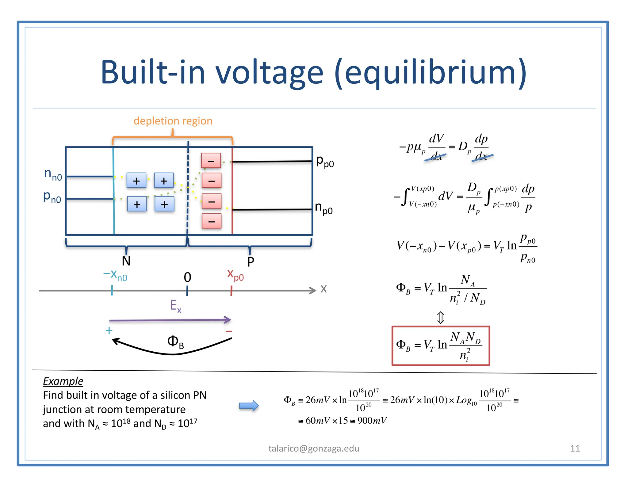
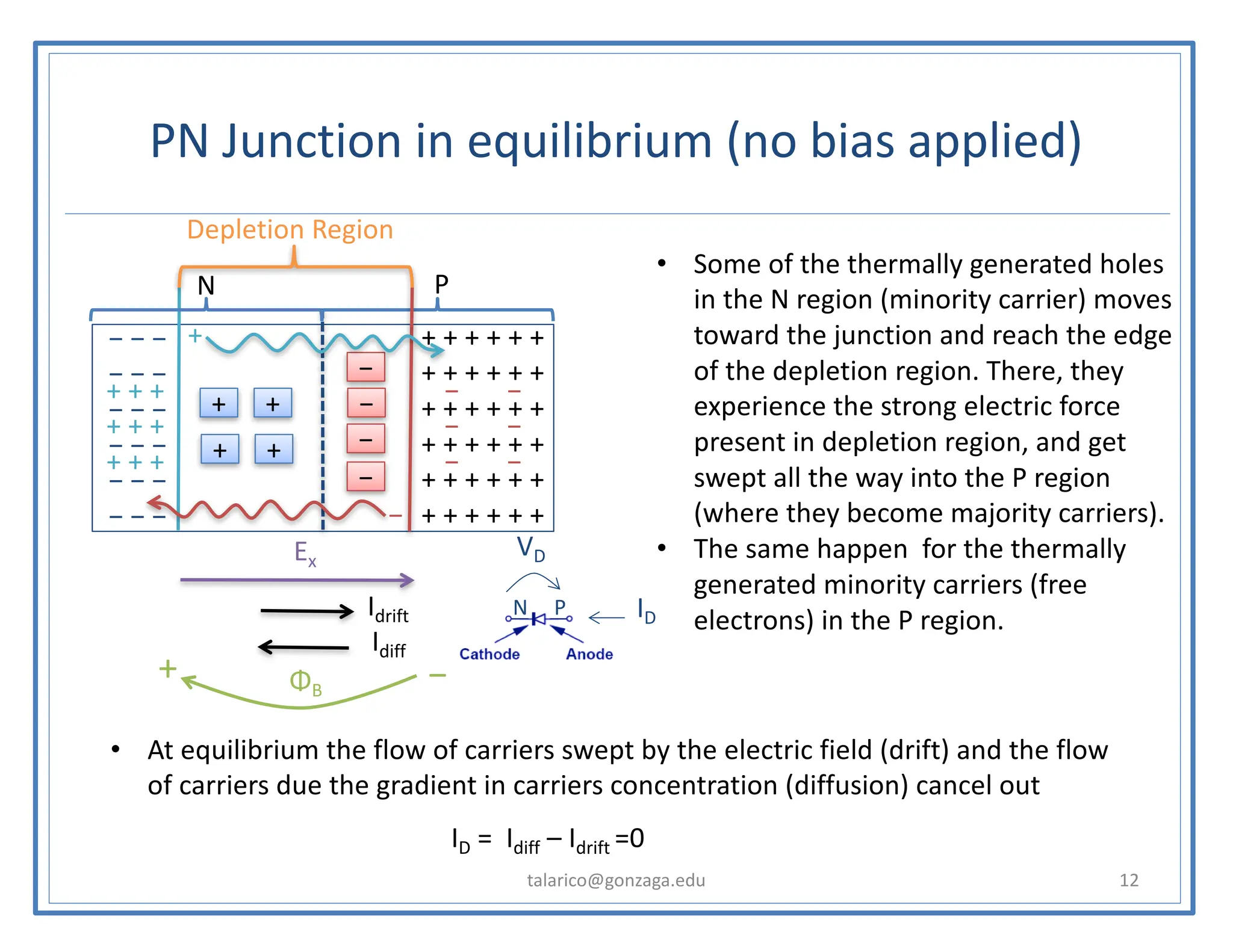
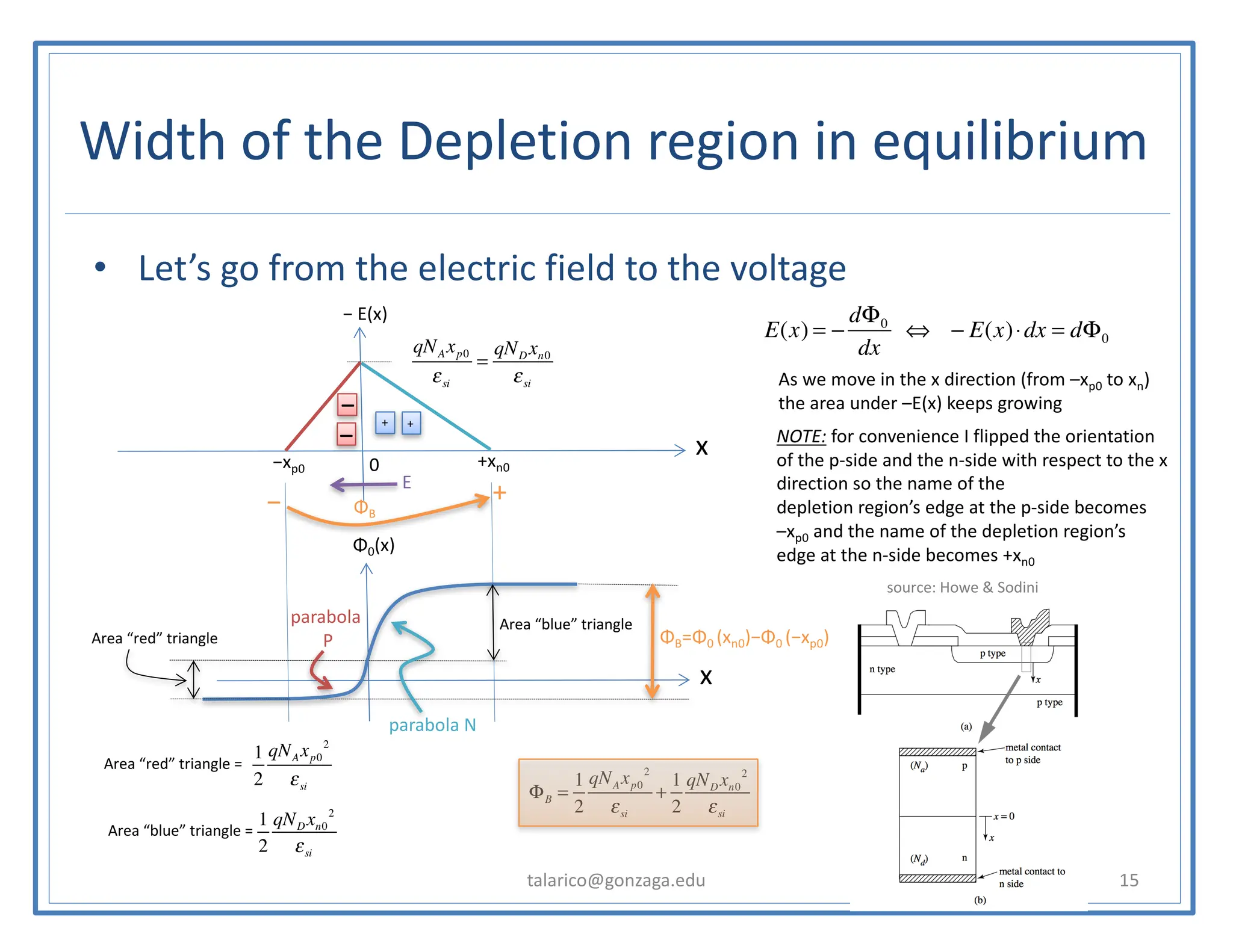
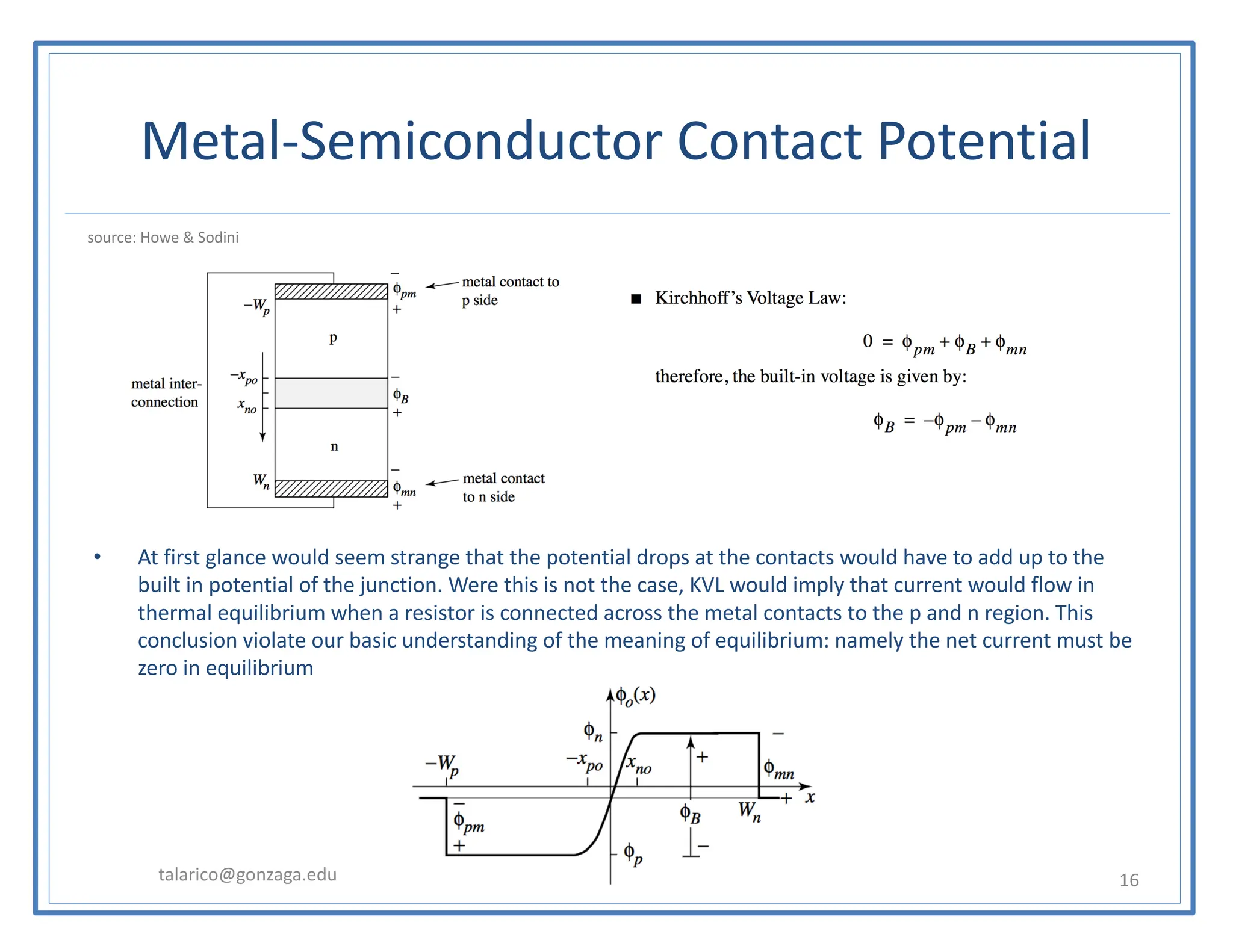
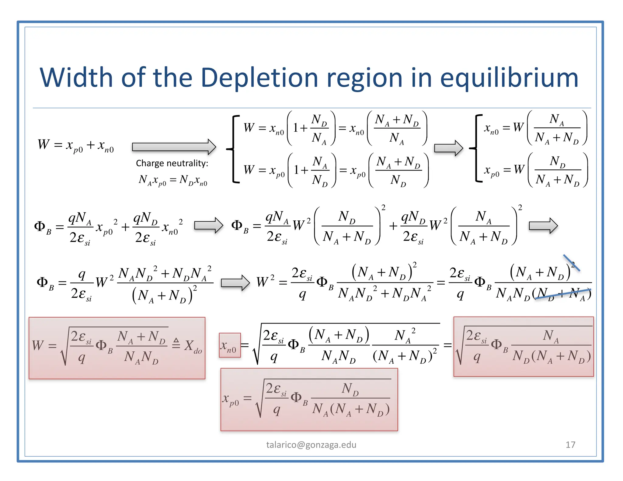
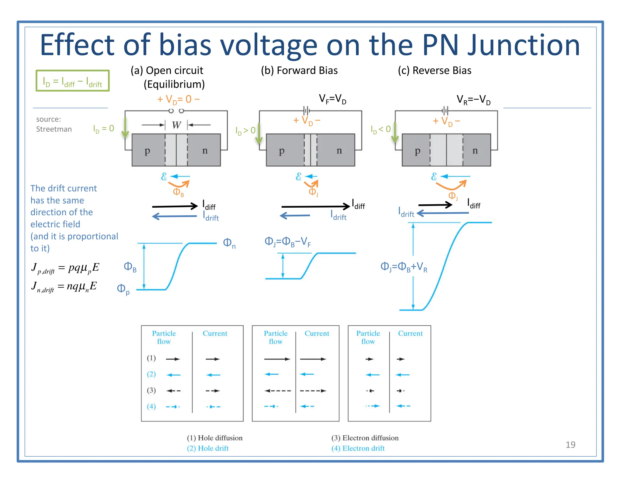
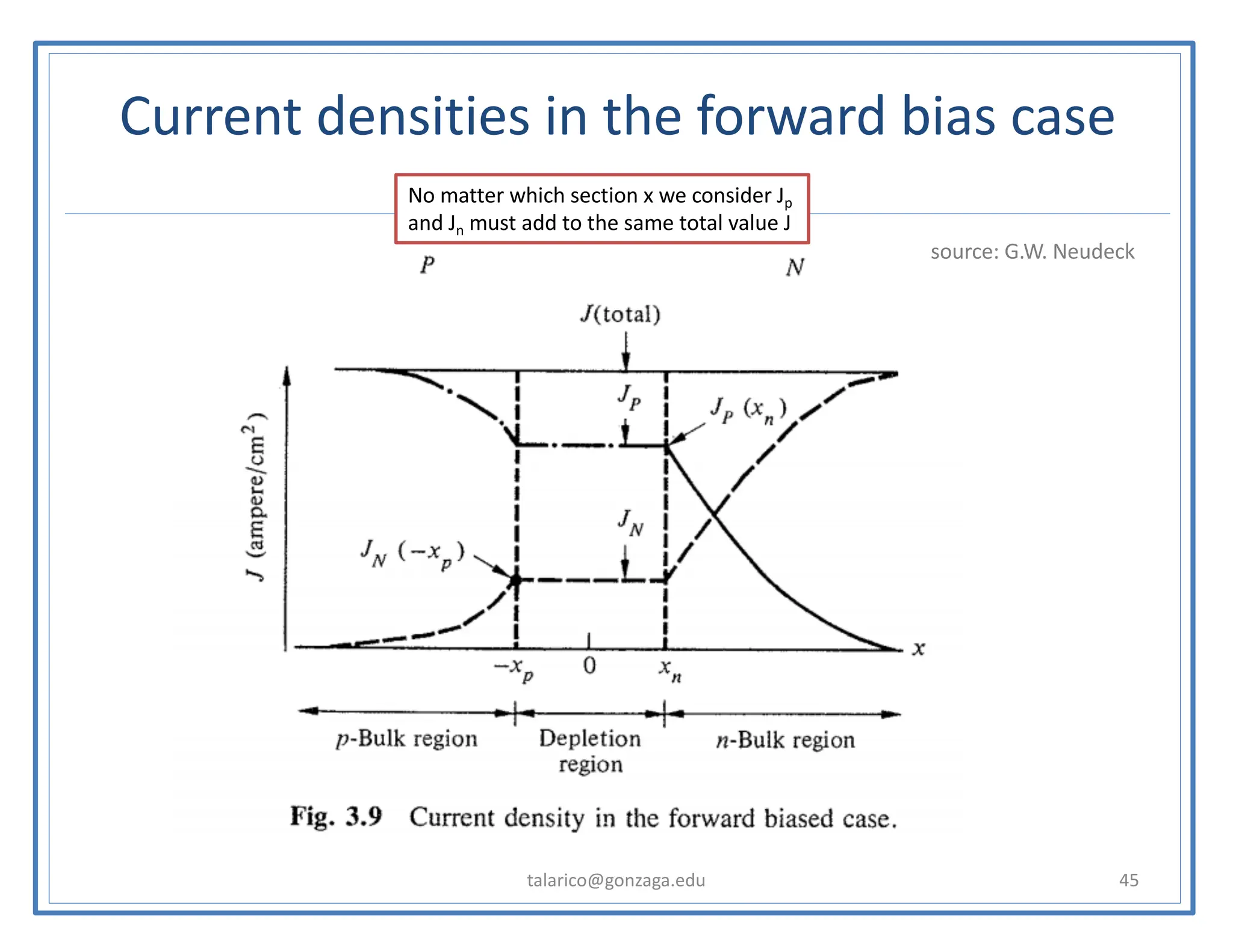
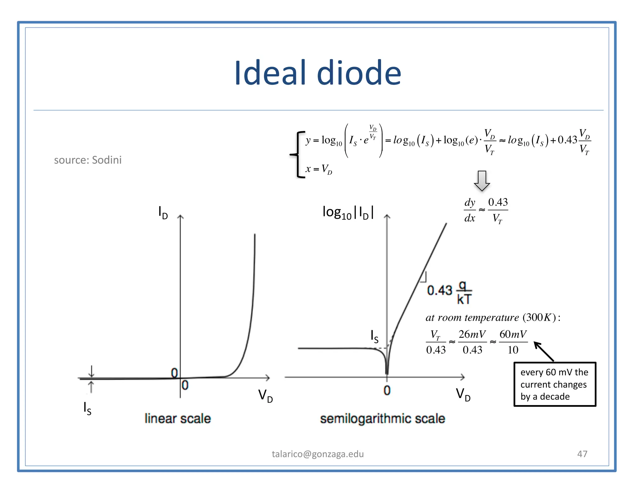
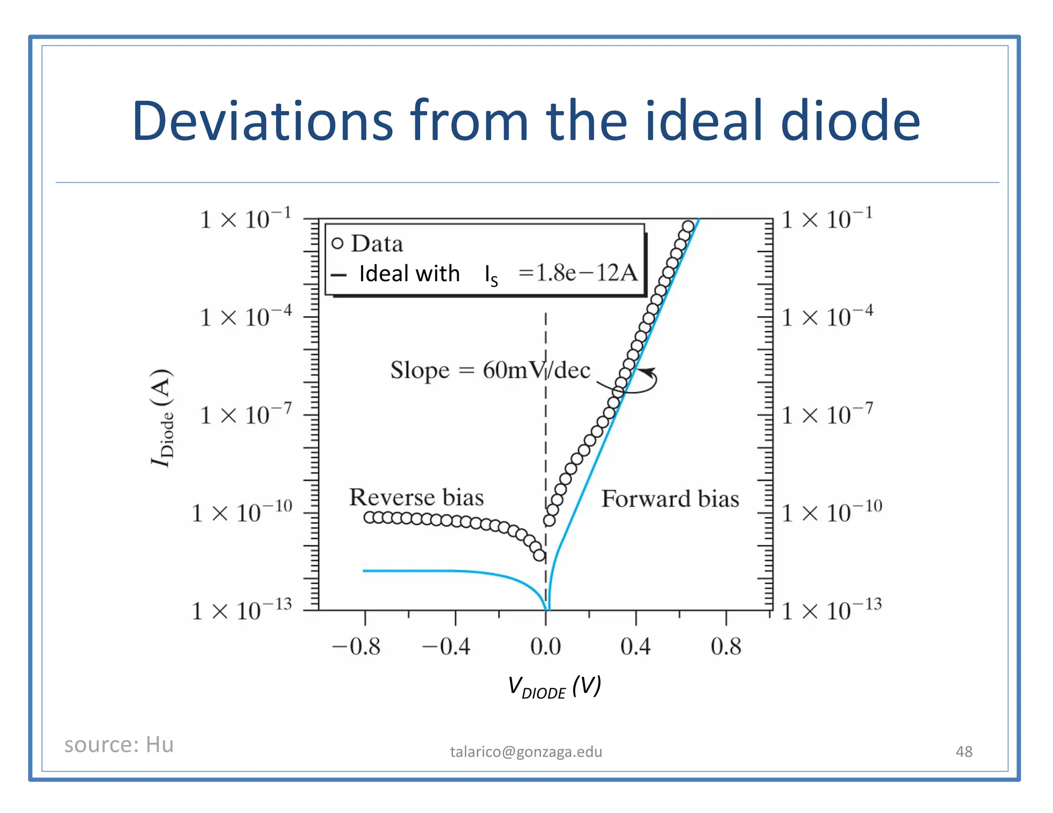
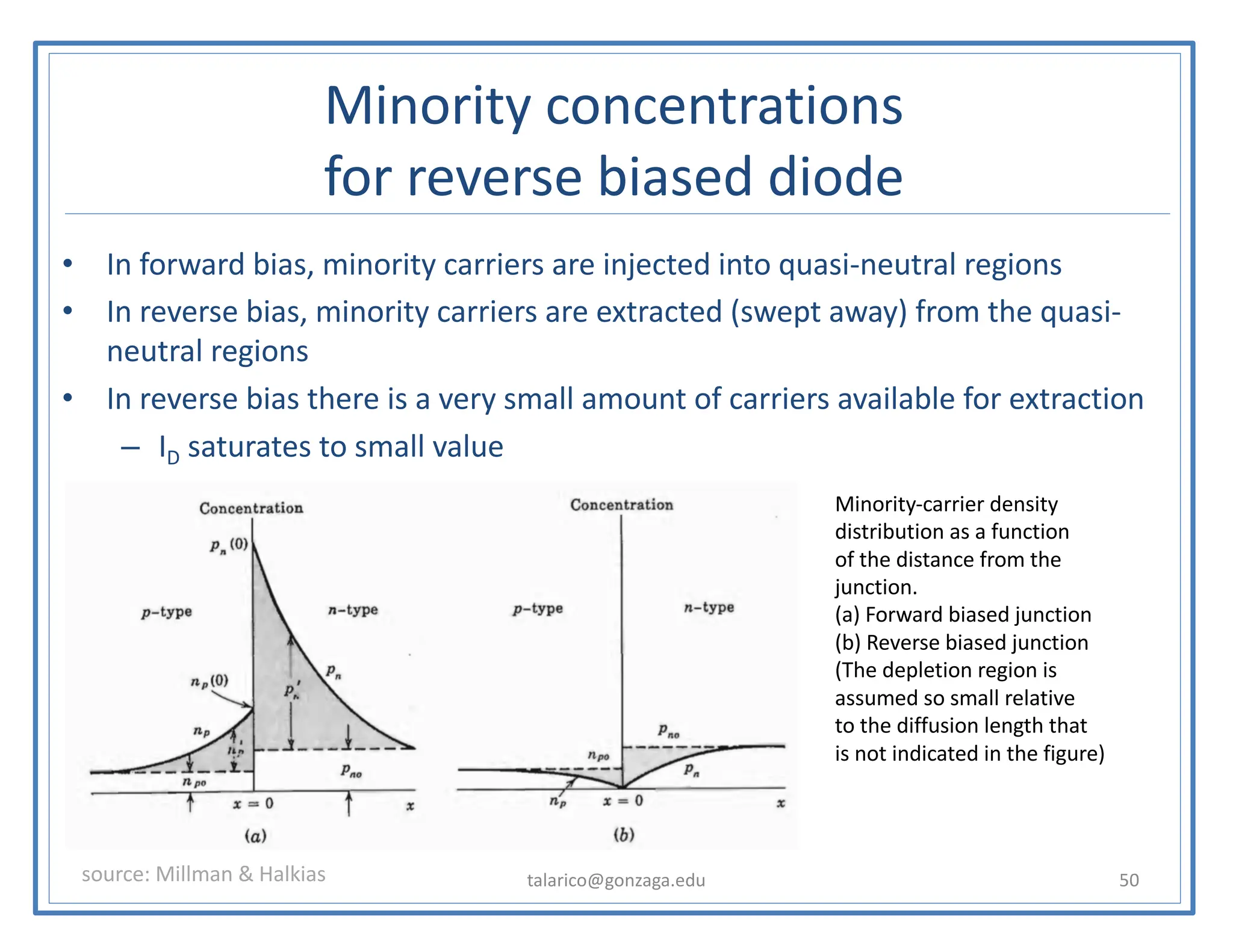
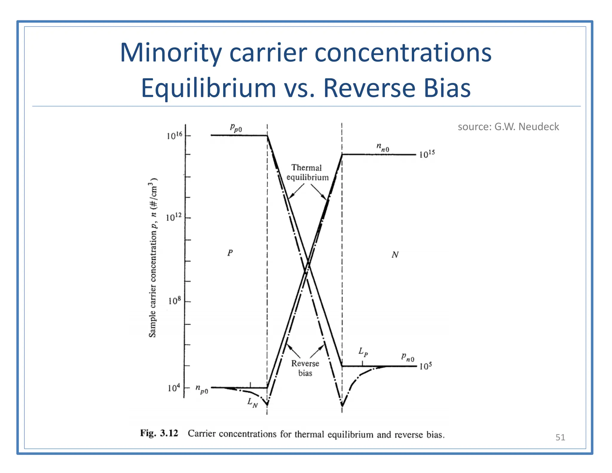
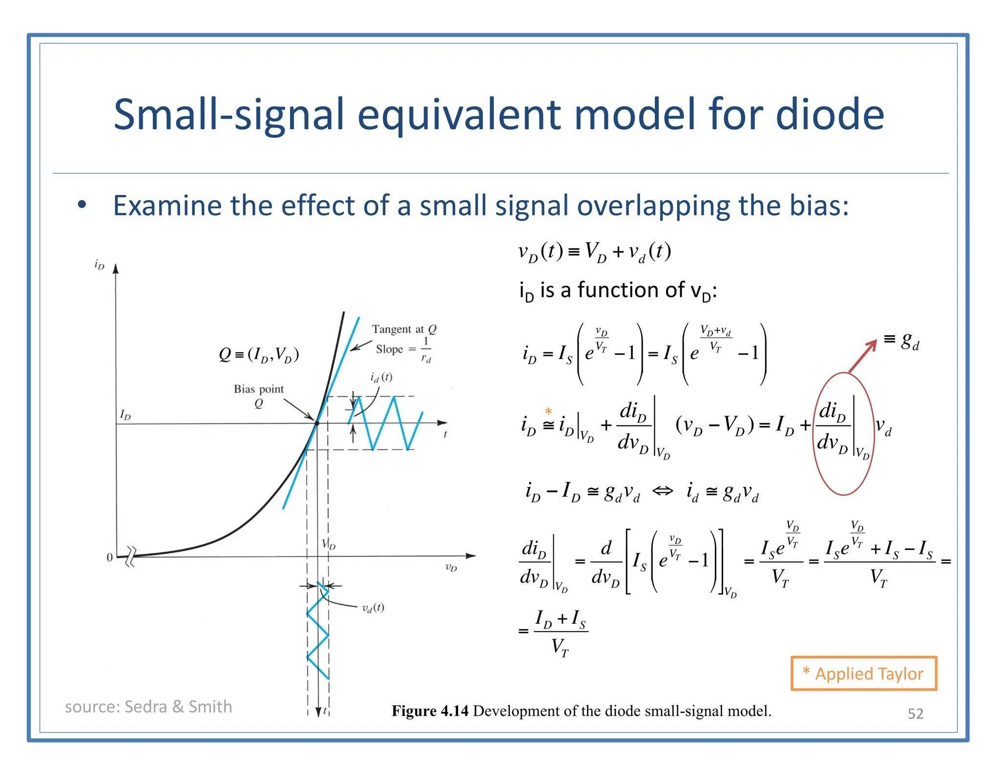
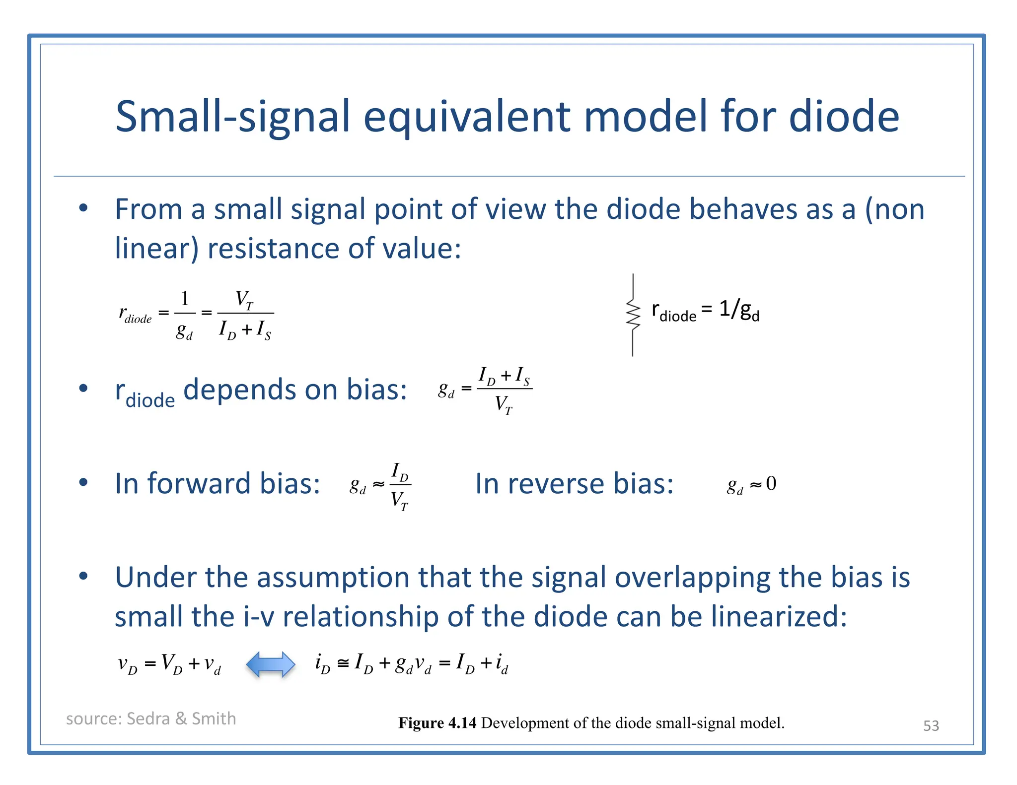
This document discusses the PN junction diode. It begins by explaining how a PN junction forms when P-type and N-type semiconductors are placed side by side. It then discusses the current-voltage characteristics of diodes in different operating regions: equilibrium (open circuit), forward bias, and reverse bias. The document goes on to explain the diffusion and drift currents that occur in the depletion region of a PN junction in equilibrium, and how these currents cancel out, resulting in no net current flow. It also discusses how the built-in voltage arises across the junction in equilibrium due to the diffusion potential.
![Width of the Depletion region in equilibrium
13
− − −
− − −
− − −
− − −
+ + + + + +
+ + + + + +
+ + + + + +
+ + + + + +
−
−
−
−
+
+
+
+
P
N
−xn0 +xp0
0
E
metal contact
A
K
metal contact
−xn0 +xp0
x
concentration [cm−3]
pp0=NA
np0≈ni
2/NA
nn0=ND
pn0≈ni
2/ND
W=Xd0
Idrift
Idiff
−xn0
x
+xp0
ρ = charge density [Cb/cm−3]
−qNA
+qND
|Q −|= qNAAxp0
|Q +|= qNDAxn0](https://image.slidesharecdn.com/ch3pnjunction-231218112829-88e67200/75/ch3_pnjunction-pptx-pdf-13-2048.jpg)
![Width of the Depletion region in equilibrium
talarico@gonzaga.edu 14
−xn0
x
+xp0
ρ = charge density [Cb/cm−3]
−qNA
+qND
|Q −|= qNAAxp0
|Q +|= qNDAxn0
Charge conservation:
|Q+ |=|Q− | ! QJ 0
"
AqND xn0 = AqNAxp0
"
ND xn0 = NAxp0
E(x)
x
−xn0 +xp0
E(0) =
−qNAxp0
εsi
=
−qND xn0
εsi
! Emax
PoissonEquation:
dE
dx
=
ρ
εsi
!
dE =
ρ
εsi
dx
As long as we know how to compute
the area of a rectangle we are fine
with the math !!!
Permittivity of crystalline silicon:
εsi ≈ 11.7×8.85×10−12 F/m
εr ε0](https://image.slidesharecdn.com/ch3pnjunction-231218112829-88e67200/75/ch3_pnjunction-pptx-pdf-14-2048.jpg)
![Charge on either side of the depletion region
(in equilibrium)
talarico@gonzaga.edu 18
QJ 0 !|Q+ |=|Q− |= AqND xn0
xn0
x
−xp0
ρ = charge density [Cb/cm−3]
−qNA
+qND
|Q −|= qNAAxp0
|Q +|= qNDAxn0
QJ 0 = AqNDW
NA
NA + ND
= Aq
NAND
NA + ND
W
QJ 0 = Aq
NAND
NA + ND
2εsi
q
ΦB
NA + ND
NAND
= A 2εsiq
NAND
NA + ND
ΦB
Junction Charge
xn0 = W
NA
NA + ND
⎛
⎝
⎜
⎞
⎠
⎟
xp0 = W
ND
NA + ND
⎛
⎝
⎜
⎞
⎠
⎟
= xn0
= W=Xd0](https://image.slidesharecdn.com/ch3pnjunction-231218112829-88e67200/75/ch3_pnjunction-pptx-pdf-18-2048.jpg)


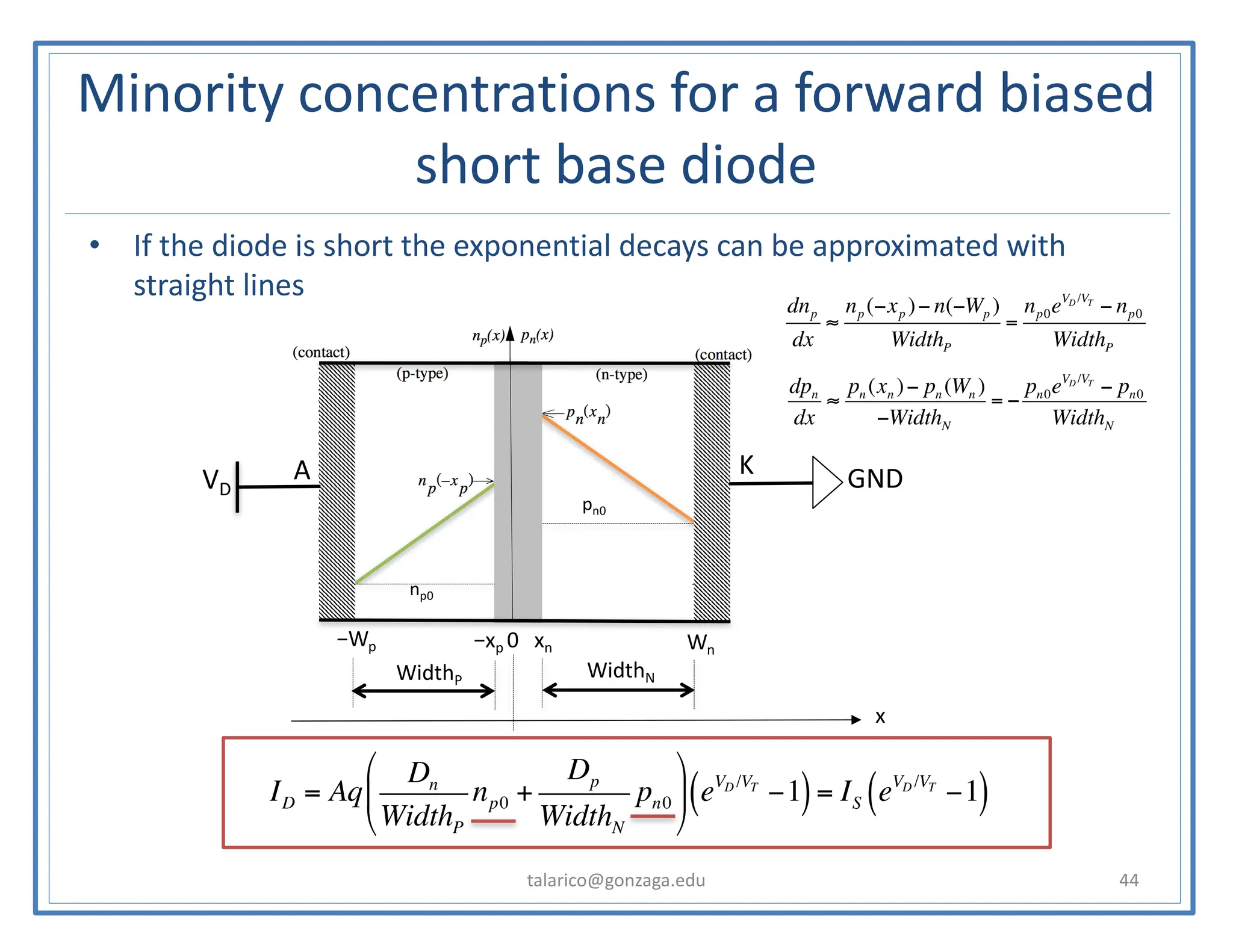
![Aside (a simple trick to simplify the math)
talarico@gonzaga.edu 39
• Change the axis selection for the bulk regions as follows:
• This way we can write the minority carriers concentrations as follows:
np (x'') = Δnpe
−
x''
Ln
pn (x') = Δpne
−
x'
Lp
x'' ! 0'' ≡ −xp
x' ! 0' ≡ xn
Ln = Dnτn
Lp = Dpτ p
source: G.W. Neudeck
source: G.W. Neudeck
Ln = Diffusion length for electrons [m]
Lp = Diffusion length for holes [m]
Dn = Diffusion coefficient for electron [m2/s]
Dp = Diffusion coefficient for holes [m2/s]
τn = mean lifetime for electrons [s]
τp = mean lifetime for holes [s]
VA = voltage applied ≡ VD](https://image.slidesharecdn.com/ch3pnjunction-231218112829-88e67200/75/ch3_pnjunction-pptx-pdf-39-2048.jpg)


![Diffusion capacitance
• Let’s examine what happen when we apply a small increase in
voltage (vD=VD+vd=VD+ΔvD)
talarico@gonzaga.edu 59
Small increase in VD
Small increase in qPn
Small increase in qNn
Behaves as a capacitor of capacitance:
n(xn) [for VD+vd]
n(xn) [for VD]
n
p
p(xn) [for VD+vd]
p(xn) [for VD]
Cdn =
dqPn
dvD vD=VD
=
qA
2
Wn − xn
( )
ni
2
Nd
1
VT
e
VD
VT](https://image.slidesharecdn.com/ch3pnjunction-231218112829-88e67200/75/ch3_pnjunction-pptx-pdf-59-2048.jpg)


![Diffusion capacitance
talarico@gonzaga.edu 63
0
−xp
−Wp
p(−xp) for VD
p
p-QNR
Na
−dqNp
n(−xp) for VD
ni
2
Na
x
n
p(−xp) for VD+vd
+dqPp
n(−xp) for VD+vd
n(xn) [for VD+vd]
n(xn) [for VD]
n
p
p(xn) [for VD+vd]
p(xn) [for VD]
−dqNn
+dqPn](https://image.slidesharecdn.com/ch3pnjunction-231218112829-88e67200/75/ch3_pnjunction-pptx-pdf-63-2048.jpg)


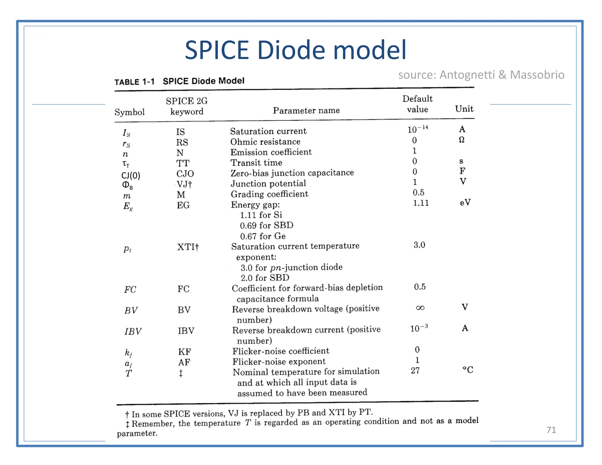
![SPICE characteristic of diode
talarico@gonzaga.edu 72
SPICE
source: Antognetti & Massobrio
Example:
D1 1 2 diode_1N4004
.model diode_1N4004 D (IS=18.8n RS=0 BV=400
+ IBV=5.00u CJO=30 M=0.333 N=2)
D2 3 4 idealmod_d
.model idealmod_d D
+ IS=10f
+ n = 0.01
+ IBV=0.1n
* By default BV = inf
General Sxntax:
D[name] <anode_node> <cathode_node> <modelname>
.model <modelname> D (<paramX>=<valueX> <paramY>=<valueY> ...)](https://image.slidesharecdn.com/ch3pnjunction-231218112829-88e67200/75/ch3_pnjunction-pptx-pdf-72-2048.jpg)