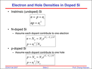
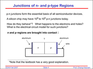
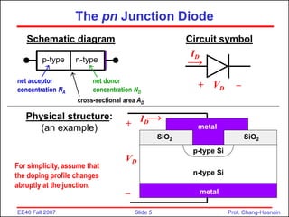
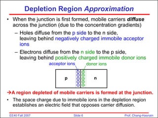
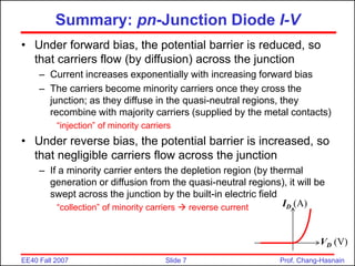
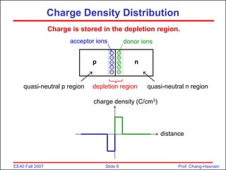
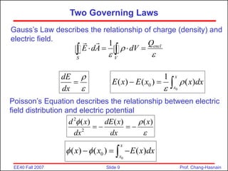
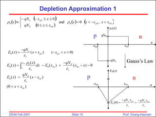
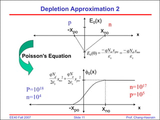
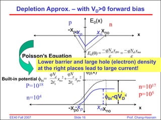
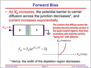
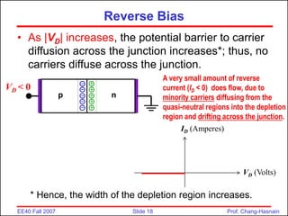
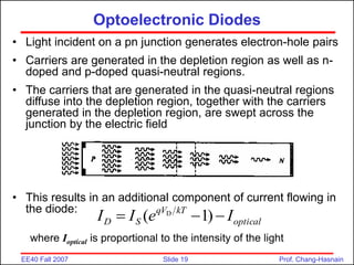
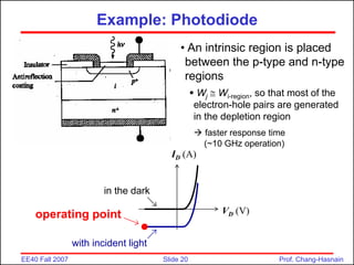
The document discusses electron and hole densities in doped silicon. It explains that pure silicon is an insulator, but can conduct when impurities are added that provide extra electrons (n-type silicon) or a deficit of electrons (p-type silicon). A pn junction is formed when n-type and p-type silicon are joined, which has interesting electrical properties and forms the basis of semiconductor devices. The document then summarizes the physics of a pn junction diode, including the depletion approximation and how applying a voltage affects carrier transport.
This document summarizes a lecture on PN junctions. It begins by discussing diffusion and how a concentration gradient causes particles to diffuse from an area of high concentration to low concentration. It then explains how bringing a p-type and n-type semiconductor together forms a PN junction. Minority carriers diffuse across the junction, leaving an electric field. The depletion approximation is introduced, where the junction region is assumed to be completely depleted of free carriers, simplifying the analysis of the electric field.
05 reverse biased junction & breakdownZerihunDemere
1. P-N diode rectifiers use the asymmetric conduction of P-N junctions to allow current in only one direction, rectifying an AC input into a pulsed DC output.
2. When a P-N junction is reverse biased, a depletion region forms where the P and N regions are depleted of mobile charge carriers. This results in a built-in electric field.
3. Under sufficient reverse bias, avalanche breakdown can occur where the built-in electric field accelerates carriers to energies high enough to liberate other carriers through impact ionization, causing an avalanche multiplication of carriers and a sharp rise in reverse current.
This document provides an overview of diodes, including:
- What materials diodes are made from, such as silicon, germanium, and gallium arsenide.
- How n-type and p-type materials are created by doping semiconductors with different elements.
- How a pn junction is formed and its properties when biased, including the depletion region.
- Diode circuit models of increasing complexity, from ideal diode to models including barrier potential and resistance.
- Key diode characteristics like the shockley equation, transconductance curve, and dynamic resistance.
- Examples of calculating diode operating points and voltage drops in circuits.
- Different types of
1. The document discusses several key concepts in electrostatics including:
2. Line integral of electric field is equal to the negative of the potential difference between two points. Work done by an external force in moving a test charge between two points is equal to the potential difference.
3. Electrostatic force is a conservative force since the work done in moving a test charge along a closed path is zero, meaning the work is independent of the path taken.
4. Conductors allow the flow of electric charge through them, while insulators do not. Dielectrics can transmit electric effects when placed in an electric field through the induction of surface charges.
Introduction to physics of-semiconductorsssuser2090f5
The document provides an introduction to the basic physics of semiconductors. It discusses semiconductor materials and their properties, including PN junction diodes. It explains that PN junctions form the basis of most semiconductor devices. When a P-type and N-type semiconductor are joined, a PN junction or diode is created. The document outlines the three operating regions of a diode: equilibrium, reverse bias, and forward bias. It describes how current flows through diffusion and drift in each bias condition and how this determines the diode's I-V characteristics. The document also briefly discusses reverse breakdown that can occur under high reverse voltages.
Ch4 lecture slides Chenming Hu Device for ICChenming Hu
The document discusses PN junctions and their properties. It covers:
1) The basic structure of a PN junction and its energy band diagram under equilibrium conditions. A depletion region forms where the bands bend.
2) The built-in potential that exists across the depletion region due to the diffusion of charge carriers. This potential can be calculated from the doping concentrations.
3) The behavior of a PN junction under forward and reverse bias, including how the depletion region width changes with applied voltage. Carrier injection also occurs under forward bias.
4) Breakdown mechanisms that can occur under high reverse bias, including avalanche and tunneling breakdown. Zener diodes are designed to operate
This document discusses PN junctions and their properties. It covers:
1) The basic structure of a PN junction, including the depletion region and built-in potential.
2) How the depletion region width, built-in potential, and electric field vary with doping concentration and applied bias.
3) Poisson's equation and how it relates charge density to the electric field in the depletion region.
4) The capacitance-voltage characteristics of a PN junction and how this can be used to determine doping concentrations.
5) Breakdown mechanisms in PN junctions including Zener tunneling and avalanche breakdown.
1. The document discusses the principles and operation of pn-junction diodes and light emitting diodes (LEDs). It describes how a depletion region forms around the pn-junction due to diffusion of holes and electrons.
2. In an LED, electron-hole pair recombination in the depletion region and surrounding areas results in photon emission. The photon energy is approximately equal to the semiconductor's band gap energy.
3. Common LED materials use direct bandgap III-V semiconductors like GaAs and GaP or their alloys. The bandgap can be tuned to emit light across the visible and infrared spectra. Proper device design and encapsulation helps extract more light from the LED.
The document discusses photodetectors and the principles of p-n junction photodiodes. It describes the depletion region of a reverse biased p-n junction and how electron-hole pairs generated by photons are separated by the electric field. It also discusses pin photodiodes and how their intrinsic region allows for higher quantum efficiency and modulation frequencies compared to p-n junction photodiodes. Absorption coefficients of various semiconductor materials are shown as well as how direct and indirect bandgap materials differ in photon absorption.
This document describes characteristics of PN junction diodes and their usage as rectifiers. It discusses:
1) How a PN junction is formed and its depletion region. Forward and reverse biasing causes majority carrier flow or inhibits diffusion current.
2) Diode operation characteristics including the ideal switch model and practical model with 0.7V forward voltage drop. Breakdown occurs above the reverse voltage rating.
3) How diodes can be used as half-wave and full-wave rectifiers to convert AC to DC, including equations for output voltage and peak inverse voltage requirements.
The document provides an overview of PN junctions and CMOS transistors. It begins by describing how PN junctions are used in CMOS, including as diodes, ESD protection, and depletion capacitors. It then discusses the components and characteristics of abrupt and graded PN junctions, including depletion regions, capacitance, and forward/reverse bias behavior. The document also covers MOS transistors, including enhancement/depletion modes, weak inversion, and layout considerations. Key concepts are graphical representations of PN junction characteristics and the factors that determine MOS transistor threshold voltage.
1.0 construction principle of operation-types and characteristics-pn junction...sarath kumar
A P-N junction forms when a P-type semiconductor is placed in contact with an N-type semiconductor. Electrons diffuse from the N-type side into the P-type side, leaving ionized donor atoms on the N-side and accepting holes on the P-side. This creates an electric field across the depletion region that prevents further diffusion. No current flows under thermal equilibrium with zero bias. A P-N junction can be forward or reverse biased by applying a voltage, which affects the barrier and current flow. P-N junctions are the basic components of many semiconductor devices like diodes, transistors, and solar cells.
This document summarizes key concepts about P-N junction diodes:
1) When a P-type and N-type semiconductor are joined, their differing band structures cause bands to bend and form a depletion region with a built-in potential barrier.
2) Applying a forward bias lowers this barrier, allowing more current by thermionic emission. Reverse bias raises the barrier, cutting off current.
3) The depletion width and built-in voltage depend on doping concentrations, extending more into the lower-doped side. Forward bias shrinks while reverse bias widens the depletion region.
4) Current flow results from a split in quasi-Fermi levels when an applied voltage makes the Fermi level
A tunnel diode or Esaki diode is a type of semiconductor that is capable of very fast operation, well into the microwave frequency region, made possible by the use of the quantum mechanical effect called tunneling.
It was invented in August 1957 by Leo Esaki when he was with Tokyo Tsushin Kogyo, now known as Sony. In 1973 he received the Nobel Prize in Physics, jointly with Brian Josephson, for discovering the electron tunneling effect used in these diodes. Robert Noyce independently came up with the idea of a tunnel diode while working for William Shockley, but was discouraged from pursuing it.[1]
These diodes have a heavily doped p–n junction only some 10 nm (100 Å) wide. The heavy doping results in a broken bandgap, where conduction band electron states on the n-side are more or less aligned with valence band hole states on the p-side
Tunnel diodes were first manufactured by Sony in 1957[2] followed by General Electric and other companies from about 1960, and are still made in low volume today.[3] Tunnel diodes are usually made from germanium, but can also be made from gallium arsenide and silicon materials. They are used in frequency converters and detectors.[4] They have negative differential resistance in part of their operating range, and therefore are also used as oscillators, amplifiers, and in switching circuits using hysteresis.
Figure 6: 8–12 GHz tunnel diode amplifier, circa 1970
In 1977, the Intelsat V satellite receiver used a microstrip tunnel diode amplifier (TDA) front-end in the 14 to 15.5 GHz band. Such amplifiers were considered state-of-the-art, with better performance at high frequencies than any transistor-based front end.[5]
The highest frequency room-temperature solid-state oscillators are based on the resonant-tunneling diode (RTD).[6]
There is another type of tunnel diode called a metal–insulator–metal (MIM) diode, but present application appears restricted to research environments due to inherent sensitivities.[7] There is also a metal–insulator–insulator–metal MIIM diode which has an additional insulator layer. The additional insulator layer allows "step tunneling" for precise diode control.[8]
This document discusses conductors and dielectrics. It defines conductors as materials that allow free movement of charges, like metals. The key properties of conductors are that the electric field inside is zero, the charge density inside is zero, and free charges exist only on the surface. These properties influence how conductors behave in external electric fields, inducing opposite charges on surfaces. The document also discusses equipotential surfaces, Poisson's and Laplace's equations, and provides examples of calculating electric fields and charge distributions for various conductor configurations.
This document discusses pn junction diodes and the derivation of the ideal diode equation. It begins by qualitatively describing current flow under equilibrium, forward bias, and reverse bias conditions. It then shows the derivation of the ideal diode equation, which models current as a function of applied voltage. The derivation involves solving diffusion equations to find minority carrier distributions and currents, and equating these at the edges of the depletion region. The document defines the saturation current I0 as the rate of thermal carrier generation within one diffusion length of the depletion region. In summary, it provides an in-depth overview of the theoretical modeling of current in an ideal pn junction diode.
The document discusses P-N junctions, which are formed at the interface between P-type and N-type semiconductors. When these materials come into contact, majority charge carriers diffuse across the junction, leaving behind charged dopant ions. This creates an electric field and depletion region across the junction. At equilibrium with no applied voltage, a built-in potential barrier forms that prevents further carrier recombination. P-N junctions can be forward or reverse biased by an external voltage, affecting the electric field and current flow. They are the basic components of many semiconductor devices such as diodes, transistors, and solar cells.
This document provides an overview of electronics and semiconductor devices and circuits. It begins with definitions of electronics and electrical and electronics. It then discusses materials used in electronics like silicon and germanium. It covers key semiconductor concepts such as the energy band gap, intrinsic and extrinsic materials, and PN junctions. It also examines the structure and characteristics of semiconductor diodes under forward and reverse bias.
A p-n junction diode consists of a p-type semiconductor joined to an n-type semiconductor. When the two materials are joined, charge carriers diffuse across the junction leaving a depletion region devoid of free carriers. This creates a built-in electric field.
When a p-n junction diode is forward biased, the depletion region narrows allowing majority carriers to flow more easily across the junction. When reverse biased, the depletion region widens blocking the flow of majority carriers and only allowing a small leakage current of minority carriers.
P-n junction diodes have applications as rectifiers, solar cells, LEDs, and are components of other semiconductor devices like transistors. The behavior of diodes is modeled by the
This document discusses semiconductor diodes and rectifiers. It begins by explaining the physical principles of semiconductors, including intrinsic semiconductors and how doping with materials like phosphorus or boron creates n-type and p-type semiconductors. When a p-type and n-type material meet, it forms a pn junction with interesting electrical properties. Diodes are made from pn junctions and exhibit asymmetric conduction, allowing current in one direction but blocking it in the other. Diode circuits and models are also covered, along with important applications like rectification where diodes are used to convert AC to DC power.
This document discusses the PN junction diode. It begins by explaining how a PN junction forms when P-type and N-type semiconductors are placed side by side. It then discusses the current-voltage characteristics of diodes in different operating regions: equilibrium (open circuit), forward bias, and reverse bias. The document goes on to explain the diffusion and drift currents that occur in the depletion region of a PN junction in equilibrium, and how these currents cancel out, resulting in no net current flow. It also discusses how the built-in voltage arises across the junction in equilibrium due to the diffusion potential.
- The document discusses magnetic fields created by electric currents. It covers the magnetic field of a moving point charge, the Biot-Savart law for calculating the magnetic field from a current-carrying wire, and an example calculation of the magnetic field from a long straight wire.
- The right hand rule is introduced for determining the direction of magnetic fields.
- Maxwell's equations for static magnetic fields in integral and differential form are presented.
Basics of semiconductor, current equation, continuity equation, injected mino...Nidhee Bhuwal
This document provides an introduction to semiconductors. It discusses topics such as the crystal structure of germanium and silicon, intrinsic and extrinsic semiconductors, carrier mobility, and diffusion currents. Equations are presented for carrier concentrations, mass action law, drift current density, and the continuity equation. Generation and recombination of charge carriers is explained. Minority carrier injection, potential variation in graded semiconductors, and the contact potential of a step graded junction are also summarized.
This document discusses power electronics for photovoltaic (solar panel) applications. It covers photovoltaic module characteristics, single-stage and dual-stage power converter topologies for connecting photovoltaic generators to electric grids or loads, and control issues like maximum power point tracking and anti-islanding techniques. Mathematical models of photovoltaic cells and modules are presented along with examples of commercial photovoltaic modules and typical grid-connected system configurations.
This document discusses the physics of a p-n junction diode. It explains that at equilibrium, a depletion region forms at the junction due to diffusion of holes and electrons, creating a built-in potential barrier. The width of the depletion region and height of the barrier depend on the doping concentrations. Forward biasing shrinks the depletion region and lowers the barrier, allowing more current to flow. Reverse biasing widens the depletion region and increases the barrier, reducing the current flow and creating an asymmetric I-V characteristic. In the next part of the course, the minority carrier diffusion equation will be solved to make these diode characteristics quantitative.
The document discusses various topics in electromagnetism including:
1) The magnetic force on a current-carrying wire due to the Lorentz force.
2) The magnetic field produced by different current configurations such as a straight wire, circular loop, and solenoid.
3) Magnetic induction and how a changing magnetic field can induce an electromotive force based on Faraday's law of induction.
Similar to cch-LecuresF07-semiconductor-animation.ppt (20)
This document provides an overview of wound healing, its functions, stages, mechanisms, factors affecting it, and complications.
A wound is a break in the integrity of the skin or tissues, which may be associated with disruption of the structure and function.
Healing is the body’s response to injury in an attempt to restore normal structure and functions.
Healing can occur in two ways: Regeneration and Repair
There are 4 phases of wound healing: hemostasis, inflammation, proliferation, and remodeling. This document also describes the mechanism of wound healing. Factors that affect healing include infection, uncontrolled diabetes, poor nutrition, age, anemia, the presence of foreign bodies, etc.
Complications of wound healing like infection, hyperpigmentation of scar, contractures, and keloid formation.
Gender and Mental Health - Counselling and Family Therapy Applications and In...PsychoTech Services
A proprietary approach developed by bringing together the best of learning theories from Psychology, design principles from the world of visualization, and pedagogical methods from over a decade of training experience, that enables you to: Learn better, faster!
ISO/IEC 27001, ISO/IEC 42001, and GDPR: Best Practices for Implementation and...PECB
Denis is a dynamic and results-driven Chief Information Officer (CIO) with a distinguished career spanning information systems analysis and technical project management. With a proven track record of spearheading the design and delivery of cutting-edge Information Management solutions, he has consistently elevated business operations, streamlined reporting functions, and maximized process efficiency.
Certified as an ISO/IEC 27001: Information Security Management Systems (ISMS) Lead Implementer, Data Protection Officer, and Cyber Risks Analyst, Denis brings a heightened focus on data security, privacy, and cyber resilience to every endeavor.
His expertise extends across a diverse spectrum of reporting, database, and web development applications, underpinned by an exceptional grasp of data storage and virtualization technologies. His proficiency in application testing, database administration, and data cleansing ensures seamless execution of complex projects.
What sets Denis apart is his comprehensive understanding of Business and Systems Analysis technologies, honed through involvement in all phases of the Software Development Lifecycle (SDLC). From meticulous requirements gathering to precise analysis, innovative design, rigorous development, thorough testing, and successful implementation, he has consistently delivered exceptional results.
Throughout his career, he has taken on multifaceted roles, from leading technical project management teams to owning solutions that drive operational excellence. His conscientious and proactive approach is unwavering, whether he is working independently or collaboratively within a team. His ability to connect with colleagues on a personal level underscores his commitment to fostering a harmonious and productive workplace environment.
Date: May 29, 2024
Tags: Information Security, ISO/IEC 27001, ISO/IEC 42001, Artificial Intelligence, GDPR
-------------------------------------------------------------------------------
Find out more about ISO training and certification services
Training: ISO/IEC 27001 Information Security Management System - EN | PECB
ISO/IEC 42001 Artificial Intelligence Management System - EN | PECB
General Data Protection Regulation (GDPR) - Training Courses - EN | PECB
Webinars: https://pecb.com/webinars
Article: https://pecb.com/article
-------------------------------------------------------------------------------
For more information about PECB:
Website: https://pecb.com/
LinkedIn: https://www.linkedin.com/company/pecb/
Facebook: https://www.facebook.com/PECBInternational/
Slideshare: http://www.slideshare.net/PECBCERTIFICATION
LAND USE LAND COVER AND NDVI OF MIRZAPUR DISTRICT, UPRAHUL
This Dissertation explores the particular circumstances of Mirzapur, a region located in the
core of India. Mirzapur, with its varied terrains and abundant biodiversity, offers an optimal
environment for investigating the changes in vegetation cover dynamics. Our study utilizes
advanced technologies such as GIS (Geographic Information Systems) and Remote sensing to
analyze the transformations that have taken place over the course of a decade.
The complex relationship between human activities and the environment has been the focus
of extensive research and worry. As the global community grapples with swift urbanization,
population expansion, and economic progress, the effects on natural ecosystems are becoming
more evident. A crucial element of this impact is the alteration of vegetation cover, which plays a
significant role in maintaining the ecological equilibrium of our planet.Land serves as the foundation for all human activities and provides the necessary materials for
these activities. As the most crucial natural resource, its utilization by humans results in different
'Land uses,' which are determined by both human activities and the physical characteristics of the
land.
The utilization of land is impacted by human needs and environmental factors. In countries
like India, rapid population growth and the emphasis on extensive resource exploitation can lead
to significant land degradation, adversely affecting the region's land cover.
Therefore, human intervention has significantly influenced land use patterns over many
centuries, evolving its structure over time and space. In the present era, these changes have
accelerated due to factors such as agriculture and urbanization. Information regarding land use and
cover is essential for various planning and management tasks related to the Earth's surface,
providing crucial environmental data for scientific, resource management, policy purposes, and
diverse human activities.
Accurate understanding of land use and cover is imperative for the development planning
of any area. Consequently, a wide range of professionals, including earth system scientists, land
and water managers, and urban planners, are interested in obtaining data on land use and cover
changes, conversion trends, and other related patterns. The spatial dimensions of land use and
cover support policymakers and scientists in making well-informed decisions, as alterations in
these patterns indicate shifts in economic and social conditions. Monitoring such changes with the
help of Advanced technologies like Remote Sensing and Geographic Information Systems is
crucial for coordinated efforts across different administrative levels. Advanced technologies like
Remote Sensing and Geographic Information Systems
9
Changes in vegetation cover refer to variations in the distribution, composition, and overall
structure of plant communities across different temporal and spatial scales. These changes can
occur natural.
How to Make a Field Mandatory in Odoo 17Celine George
In Odoo, making a field required can be done through both Python code and XML views. When you set the required attribute to True in Python code, it makes the field required across all views where it's used. Conversely, when you set the required attribute in XML views, it makes the field required only in the context of that particular view.
This presentation was provided by Racquel Jemison, Ph.D., Christina MacLaughlin, Ph.D., and Paulomi Majumder. Ph.D., all of the American Chemical Society, for the second session of NISO's 2024 Training Series "DEIA in the Scholarly Landscape." Session Two: 'Expanding Pathways to Publishing Careers,' was held June 13, 2024.
Walmart Business+ and Spark Good for Nonprofits.pdfTechSoup
"Learn about all the ways Walmart supports nonprofit organizations.
You will hear from Liz Willett, the Head of Nonprofits, and hear about what Walmart is doing to help nonprofits, including Walmart Business and Spark Good. Walmart Business+ is a new offer for nonprofits that offers discounts and also streamlines nonprofits order and expense tracking, saving time and money.
The webinar may also give some examples on how nonprofits can best leverage Walmart Business+.
The event will cover the following::
Walmart Business + (https://business.walmart.com/plus) is a new shopping experience for nonprofits, schools, and local business customers that connects an exclusive online shopping experience to stores. Benefits include free delivery and shipping, a 'Spend Analytics” feature, special discounts, deals and tax-exempt shopping.
Special TechSoup offer for a free 180 days membership, and up to $150 in discounts on eligible orders.
Spark Good (walmart.com/sparkgood) is a charitable platform that enables nonprofits to receive donations directly from customers and associates.
Answers about how you can do more with Walmart!"
BÀI TẬP BỔ TRỢ TIẾNG ANH LỚP 9 CẢ NĂM - GLOBAL SUCCESS - NĂM HỌC 2024-2025 - ...
cch-LecuresF07-semiconductor-animation.ppt
1. Slide 1
EE40 Fall 2007 Prof. Chang-Hasnain
EE40
Lecture 32
Prof. Chang-Hasnain
11/21/07
Reading: Supplementary Reader
2. Slide 2
EE40 Fall 2007 Prof. Chang-Hasnain
Electron and Hole Densities in Doped Si
( )
2
v f
E E kT
a v
i a
p N N e
p n N
• Instrinsic (undoped) Si
• N-doped Si
– Assume each dopant contribute to one electron
• p-doped Si
– Assume each dopant contribute to one hole
( )
2
f c
E E kT
d c
i d
n N N e
p n N
2
i
i
n p n
np n
3. Slide 3
EE40 Fall 2007 Prof. Chang-Hasnain
Summary of n- and p-type silicon
Pure silicon is an insulator. At high temperatures it conducts
weakly.
If we add an impurity with extra electrons (e.g. arsenic,
phosphorus) these extra electrons are set free and we have a
pretty good conductor (n-type silicon).
If we add an impurity with a deficit of electrons (e.g. boron) then
bonding electrons are missing (holes), and the resulting holes
can move around … again a pretty good conductor (p-type
silicon)
Now what is really interesting is when we join n-type and p-type
silicon, that is make a pn junction. It has interesting electrical
properties.
4. Slide 4
EE40 Fall 2007 Prof. Chang-Hasnain
Junctions of n- and p-type Regions
A silicon chip may have 108 to 109 p-n junctions today.
p-n junctions form the essential basis of all semiconductor devices.
How do they behave*? What happens to the electrons and holes?
What is the electrical circuit model for such junctions?
n and p regions are brought into contact :
n p
aluminum
aluminum
wire
?
*Note that the textbook has a very good explanation.
5. Slide 5
EE40 Fall 2007 Prof. Chang-Hasnain
The pn Junction Diode
Schematic diagram
p-type n-type
ID
+ VD –
Circuit symbol
Physical structure:
(an example)
p-type Si
n-type Si
SiO2
SiO2
metal
metal
ID
+
VD
–
net donor
concentration ND
net acceptor
concentration NA
For simplicity, assume that
the doping profile changes
abruptly at the junction.
cross-sectional area AD
6. Slide 6
EE40 Fall 2007 Prof. Chang-Hasnain
• When the junction is first formed, mobile carriers diffuse
across the junction (due to the concentration gradients)
– Holes diffuse from the p side to the n side,
leaving behind negatively charged immobile acceptor
ions
– Electrons diffuse from the n side to the p side,
leaving behind positively charged immobile donor ions
A region depleted of mobile carriers is formed at the junction.
• The space charge due to immobile ions in the depletion region
establishes an electric field that opposes carrier diffusion.
Depletion Region Approximation
+
+
+
+
+
–
–
–
–
–
p n
acceptor ions donor ions
7. Slide 7
EE40 Fall 2007 Prof. Chang-Hasnain
Summary: pn-Junction Diode I-V
• Under forward bias, the potential barrier is reduced, so
that carriers flow (by diffusion) across the junction
– Current increases exponentially with increasing forward bias
– The carriers become minority carriers once they cross the
junction; as they diffuse in the quasi-neutral regions, they
recombine with majority carriers (supplied by the metal contacts)
“injection” of minority carriers
• Under reverse bias, the potential barrier is increased, so
that negligible carriers flow across the junction
– If a minority carrier enters the depletion region (by thermal
generation or diffusion from the quasi-neutral regions), it will be
swept across the junction by the built-in electric field
“collection” of minority carriers reverse current ID (A)
VD (V)
8. Slide 8
EE40 Fall 2007 Prof. Chang-Hasnain
quasi-neutral p region
Charge Density Distribution
+
+
+
+
+
–
–
–
–
–
p n
acceptor ions donor ions
depletion region quasi-neutral n region
charge density (C/cm3)
distance
Charge is stored in the depletion region.
9. Slide 9
EE40 Fall 2007 Prof. Chang-Hasnain
Two Governing Laws
2
2
( ) ( ) ( )
d x dE x x
dx dx
0
0
1
( ) ( ) ( )
x
x
E x E x x dx
dE
dx
1 encl
S V
Q
E dA dV
Gauss’s Law describes the relationship of charge (density) and
electric field.
Poisson’s Equation describes the relationship between electric
field distribution and electric potential
0
0
( ) ( ) ( )
x
x
x x E x dx
10. Slide 10
EE40 Fall 2007 Prof. Chang-Hasnain
Depletion Approximation 1
0 ( ) ( ) ( 0)
a
po po
s
qN
E x x x x x
0
0
0
0
0
0 ,
0
and
0
0
n
p
n
d
p
a
x
x
x
x
x
x
x
qN
x
x
qN
x
xno
x
x
-xpo
ρo(x)
-qNa
qNd
xno x
x
-xpo
E0(x)
s
no
d
s
po
a x
qN
x
qN
E
)
0
(
0
0
0 0
0
( )
( ) ( ) ( ) 0
( ) ( )
(0 )
no
x
d
no no
x
s s
d
no
s
no
x qN
E x dx E x x x
qN
E x x x
x x
Gauss’s Law
p n
p n
11. Slide 11
EE40 Fall 2007 Prof. Chang-Hasnain
Depletion Approximation 2
p n
P=1018
n=104
n=1017
p=105
x
E0(x)
s
no
d
s
po
a x
qN
x
qN
E
)
0
(
0
xno
-xpo
2
2
2
2 po
s
a
no
s
d
x
qN
x
qN
0(x)
x
xno
-xpo
Poisson’s Equation
12. Slide 12
EE40 Fall 2007 Prof. Chang-Hasnain
EE40
Lecture 33
Prof. Chang-Hasnain
11/26/07
Reading: Supplementary Reader
13. Slide 13
EE40 Fall 2007 Prof. Chang-Hasnain
Depletion Approximation 3
0 0 0
( ) ( ) ( ) ( ) 0
po po
po po
x x
a
po po
x x
s
x x
a
po
x x
s
qN
x E x dx x x x dx
qN
xdx x dx
2
0 ( ) ( ) ( 0)
2
a
po po
s
qN
x x x x x
2
0 0 0
0 0
2
0 0
( ) ( ) (0) ( ) (0 )
2
2
x x
d a
no po
s s
x x
d a
no po
s s
qN qN
x E x dx x x dx x
qN qN
x dx x dx x
2 2
0 ( ) (2 ) (0 )
2 2
d a
no po no
s s
qN qN
x x x x x x x
14. Slide 14
EE40 Fall 2007 Prof. Chang-Hasnain
Effect of Applied Voltage
• The quasi-neutral p and n regions have low resistivity,
whereas the depletion region has high resistivity. Thus,
when an external voltage VD is applied across the
diode, almost all of this voltage is dropped across
the depletion region. (Think of a voltage divider
circuit.)
• If VD > 0 (forward bias), the potential barrier to carrier
diffusion is reduced by the applied voltage.
• If VD < 0 (reverse bias), the potential barrier to carrier
diffusion is increased by the applied voltage.
p n
+
+
+
+
+
–
–
–
–
–
VD
15. Slide 15
EE40 Fall 2007 Prof. Chang-Hasnain
Depletion Approx. – with VD<0 reverse bias
p n
P=1018
n=1017
x
E0(x)
s
no
d
s
po
a x
qN
x
qN
E
)
0
(
0
xno
-xpo
2
2
2
2 po
s
a
no
s
d
x
qN
x
qN
0(x)
x
xno
-xpo
bi
Built-in potential bi=
-xp xn
-xp xn
bi-qVD
Higher barrier and few holes in n-
type lead to little current! p=105
n=104
16. Slide 16
EE40 Fall 2007 Prof. Chang-Hasnain
Depletion Approx. – with VD>0 forward bias
Poisson’s Equation
p n
n=104
n=1017
p=105
x
E0(x)
s
no
d
s
po
a x
qN
x
qN
E
)
0
(
0
xno
-xpo
2
2
2
2 po
s
a
no
s
d
x
qN
x
qN
0(x)
x
xno
-xpo
bi
Built-in potential bi=
-xp xn
bi-qVD
Lower barrier and large hole (electron) density
at the right places lead to large current!
-xp xn
P=1018
17. Slide 17
EE40 Fall 2007 Prof. Chang-Hasnain
Forward Bias
• As VD increases, the potential barrier to carrier
diffusion across the junction decreases*, and
current increases exponentially.
ID (Amperes)
VD (Volts)
* Hence, the width of the depletion region decreases.
p n
+
+
+
+
+
–
–
–
–
–
VD > 0
The carriers that diffuse across the
junction become minority carriers in
the quasi-neutral regions; they then
recombine with majority carriers,
“dying out” with distance.
D
( 1)
qV kT
D S
I I e
18. Slide 18
EE40 Fall 2007 Prof. Chang-Hasnain
Reverse Bias
• As |VD| increases, the potential barrier to carrier
diffusion across the junction increases*; thus, no
carriers diffuse across the junction.
ID (Amperes)
VD (Volts)
* Hence, the width of the depletion region increases.
p n
+
+
+
+
+
–
–
–
–
–
VD < 0
A very small amount of reverse
current (ID < 0) does flow, due to
minority carriers diffusing from the
quasi-neutral regions into the depletion
region and drifting across the junction.
19. Slide 19
EE40 Fall 2007 Prof. Chang-Hasnain
• Light incident on a pn junction generates electron-hole pairs
• Carriers are generated in the depletion region as well as n-
doped and p-doped quasi-neutral regions.
• The carriers that are generated in the quasi-neutral regions
diffuse into the depletion region, together with the carriers
generated in the depletion region, are swept across the
junction by the electric field
• This results in an additional component of current flowing in
the diode:
where Ioptical is proportional to the intensity of the light
optical
kT
V
q
S
D I
e
I
I
)
1
( D
Optoelectronic Diodes
20. Slide 20
EE40 Fall 2007 Prof. Chang-Hasnain
Example: Photodiode
• An intrinsic region is placed
between the p-type and n-type
regions
Wj Wi-region, so that most of the
electron-hole pairs are generated
in the depletion region
faster response time
(~10 GHz operation)
ID (A)
VD (V)
with incident light
in the dark
operating point
21. Slide 21
EE40 Fall 2007 Prof. Chang-Hasnain
Planck Constant
• Planck’s constant h = 6.625·10-34 J·s
• E=hnhc/l1.24 eV-mm/lmm)
• C is speed of light and hn is photon energy
• The first type of quantum effect is the quantization of
certain physical quantities.
• Quantization first arose in the mathematical formulae of
Max Planck in 1900. Max Planck was analyzing how the
radiation emitted from a body was related to its
temperature, in other words, he was analyzing the
energy of a wave.
• The energy of a wave could not be infinite, so Planck
used the property of the wave we designate as the
frequency to define energy. Max Planck discovered a
constant that when multiplied by the frequency of any
wave gives the energy of the wave. This constant is
referred to by the letter h in mathematical formulae. It is
a cornerstone of physics.
22. Slide 22
EE40 Fall 2007 Prof. Chang-Hasnain
Bandgap Versus Lattice Constant
Si