Download to read offline
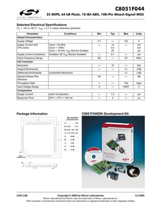
![C8051F044
25 MIPS, 64 kB Flash, 10-Bit ADC, 100-Pin Mixed-Signal MCU
Analog Peripherals High-Speed 8051 µC Core
10-Bit ADC - Pipelined instruction architecture; executes 70% of instructions in 1 or 2
- ±1 LSB INL; guaranteed monotonic system clocks
- Programmable throughput up to 100 ksps - Up to 25 MIPS throughput with 25 MHz system clock
- 13 external inputs; programmable as single-ended or differential - Expanded interrupt handler
- Programmable amplifier gain: 16, 8, 4, 2, 1, 0.5 Memory
- Data-dependent windowed interrupt generator - 4352 bytes data RAM
- Built-in temperature sensor (±3 °C) - 64 kB Flash; in-system programmable in 512-byte sectors (512 bytes
High-Voltage Differential Amplifier are reserved)
- 60 V common mode input range
- External parallel data memory interface
- Offset adjust from –60 to +60 V CAN Bus 2.0B
- 16 gain settings from 0.05 to 16 - 32 message objects
Three Comparators - ”Mailbox" implementation only interrupts CPU when needed
Internal Voltage Reference Digital Peripherals
Precision VDD Monitor/Brown-out Detector - 64 port I/O; all are 5 V tolerant
On-Chip JTAG Debug & Boundary Scan - Hardware SMBus™ (I2C™ compatible), SPI™, and two UART serial
- On-chip debug circuitry facilitates full speed, non-intrusive in-system ports available concurrently
debug (no emulator required) - Programmable 16-bit counter array with 6 capture/compare modules
- Provides breakpoints, single stepping, watchpoints, stack monitor, pro- - 5 general-purpose 16-bit counter/timers
gram trace memory - Dedicated watchdog timer; bidirectional reset
- Inspect/modify memory and registers - Real-time clock mode using timer 3 or PCA
- Superior performance to emulation systems using ICE-chips, target Clock Sources
pods, and sockets
- IEEE1149.1 compliant boundary scan - Internal programmable 2% oscillator: up to 25 MHz
Supply Voltage: 2.7 to 3.6 V - External oscillator: Crystal, RC, C, or Clock
- Typical operating current: 10 mA at 25 MHz
Package
- Multiple power saving sleep and shutdown modes - 100-pin TQFP (standard lead and lead-free packages)
Temperature Range: –40 to +85 °C Ordering Part Numbers
- Lead-free package: C8051F044-GQ
- Standard package: C8051F044
VDD
VDD Digital Power
UART0 P0 P0.0
8
VDD
DGND UART1 Drv P0.7
DGND
DGND
SFR Bus SMBus C
AV+
AV+ Analog Power 0 SPI Bus
R P1 P1.0
AV+ O Drv P1.7
AGND
AGND
AGND
5 PCA
Timers
S
S P2.0/CPx
TCK
TMS
TDI
JTAG
Logic
Boundary Scan
Debug HW
1 0,1,2,3,4
B
A
P2
Drv P2.7/CPx
TDO Port
RST Reset 64 kB 0,1,2,3 R
&4 P3.0/AINAMUX0
FLASH P3
Latches Drv
MONEN
VDD
Monitor
WDT C 32x136
P3.7/AINAMUX7
CAN CANTX
XTAL1
XTAL2
External
Oscillator
o CANRAM
2.0B CANRX
Circuit 256 byte
r
System
Clock
VREF VREF
RAM
Internal
e 4 kB
XRAM +
P2.0
CP0 P2.1
2% -
P2.2
Oscillator +
CP1 P2.3
-
P2.4
+
CP2 P2.5
VREF0 -
AIN0.0
AIN0.1
AIN0.2
AIN0.3 P4.0
A ADC Port 4 <from crossbar> P4 P4.4
M Prog
100 ksps DRV P4.5/ALE
U Gain
External Data Memory Bus Bus Control
Ctrl Latch
P4.6/RD
X (10-Bit) P4.7/WR
P5 Latch P5.0/A0
P5
Address [15:0]
TEMP
SENSOR Addr [7:0] DRV P5.7/A7
A P6 Latch P6.0/A8
P6
M 8:2
Addr [15:8] DRV P6.7/A15
U
X P7.0/D0
HVAIN+ P7 Latch P7
HVAMP Data [7:0] DRV
Data Latch P7.7/D7
HVAIN-
HVREF
HVCAP
CAN 2.0B Copyright © 2005 by Silicon Laboratories 5.5.2005](https://image.slidesharecdn.com/8051f044-121114120603-phpapp01/85/8051f044-1-320.jpg)

The document summarizes the features of the C8051F044 microcontroller, which includes: - A 10-bit analog-to-digital converter that can operate up to 100 ksps with ±1 LSB INL. - An 8051 microcontroller core that can operate up to 25 MIPS at 25 MHz. - 64kB of flash memory and 4352 bytes of data RAM. - Peripherals including CAN 2.0B, SMBus, SPI, UART, and timers. - Packaged in a 100-pin TQFP package.


