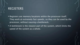
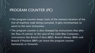
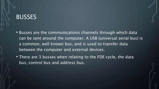
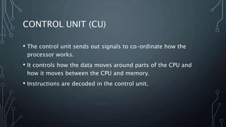
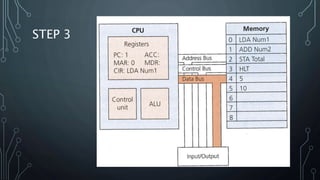
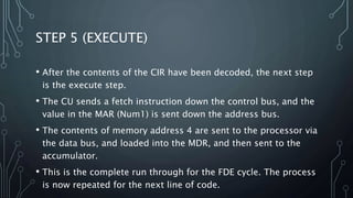
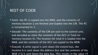
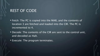
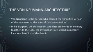
3. REGISTERS
• Registers are memory locations within the processor itself.
They work at extremely fast speeds, so they can be used by the
processor, without causing a bottleneck.
• A bottleneck is the slowest part of the system, which limits the
speed of the system as a whole.
4. PROGRAM COUNTER (PC)
• The program counter keeps track of the memory location of the
line of machine code being executed. It gets incremented, to
point to the next instruction.
• The program counter is also changed by instructions that alter
the flow of control. In the case of the Little Man Computer,
instructions like Branch if Zero (BRZ), Branch Always (BRA) and
Branch if Positive (BRP) can move the program counter
backwards or forwards.
5. MEMORY DATA REGISTER (MDR)
• The memory data register stores the data that has been fetched
from or stored in the memory.
6. MEMORY ADDRESS REGISTER
• The memory address register stores the address of the data or
instructions that are to be fetched from, or sent to.
7. CURRENT INSTRUCTION REGISTER (CIR)
• The current instruction register stores the most recently
fetched instruction, waiting to be decoded and executed.
8. ACCUMULATOR (ACC)
• The accumulator stores the results of calculations made by the
ALU.
• In the Little Man Computer, the instruction LDA loads the
contents of a given memory location into the accumulator, and
STA stores the contents of the accumulator in a given memory
location.
9. GENERAL PURPOSE REGISTERS
• Processors may also have general purpose registers.
• These can be used temporarily to store data being used rather
than sensing data to and from the comparatively much slower
memory.
10. BUSSES
• Busses are the communications channels through which data
can be sent around the computer. A USB (universal serial bus) is
a common, well known bus, and is used to transfer data
between the computer and external devices.
• There are 3 busses when relating to the FDE cycle, the data
bus, control bus and address bus.
11. WHAT DO THE BUSES DO IN THE FDE CYCLE
• The data bus carries data between the processor and memory.
• The address bus carries the address of the memory location
being read from or written to.
• And the control bus sends control signals from the control unit.
12. ARITHMETIC LOGIC UNIT (ALU)
• The ALU carries out the calculations and logical decisions.
• The results of its calculations are stored in the accumulator.
13. CONTROL UNIT (CU)
• The control unit sends out signals to co-ordinate how the
processor works.
• It controls how the data moves around parts of the CPU and
how it moves between the CPU and memory.
• Instructions are decoded in the control unit.
15. STEP 1 (FETCH)
• The first step in this set of instructions is to fetch the first
instruction from the memory.
• The program counter starts at 0 0(the program counter actually
points to the next instruction to be executed, but at the start of
the program, the next instruction is 0), and the value 0 is
loaded into the memory address register (MAR).
• The control unit (CU) then sends a fetch command, via the
control bus, and the value 0 is sent down the address bus,
meaning fetch the contents of memory location 0.
17. STEP 2
• The contents of location 0 (LDA Num1) are sent down the data
bus. This data is then stored in the memory data register
(MDR), and then moved to the current instruction register (CIR).
21. STEP 4 (DECODE)
• For the current instruction, the fetch step is complete, the next
step is the decode step.
• The contents of the CIR are sent to the CU.
• The CU decodes the instruction LDA Num1 as load the contents
of Num1 into the accumulator.
• As the program will be executing the instruction on Num1, this
location will be loaded onto the MAR.
23. STEP 5 (EXECUTE)
• After the contents of the CIR have been decoded, the next step
is the execute step.
• The CU sends a fetch instruction down the control bus, and the
value in the MAR (Num1) is sent down the address bus.
• The contents of memory address 4 are sent to the processor via
the data bus, and loaded into the MDR, and then sent to the
accumulator.
• This is the complete run through for the FDE cycle. The process
is now repeated for the next line of code.
25. REST OF CODE
• Fetch: The PC is copied to the MAR. The contents of memory
location 1 are loaded onto the CIR. The PC is incremented.
• Decode: The contents of the CIR are sent to the control unit,
and decoded as add the contents of Num2 (location 5) to the
contents of the accumulator.
• Execute: The contents of memory location 5 are fetched from
memory and loaded into the MDR, and then to the ALU.
26. REST OF CODE
• Fetch: the PC is copied into the MAR, and the contents of
memory location 2 are fetched and loaded into the CIR. The PC
is incremented to 3.
• Decode: The contents of the CIR are sent to the control unit,
and decoded as store the contents of the ACC in Total (in
memory location 6). The location for total 6 is loaded into the
MAR, and the contents of the ACC are copied to the MDR.
• Execute: A write signal is sent down the control bus, the
location 6 is sent down the address bus and the contents of the
MDR (15) is sent down the data bus. This results in the value 15
27. REST OF CODE
• Fetch: The PC is copied into the MAR, and the contents of
location 3 are fetched and loaded into the CIR. The PC is
incremented to 4.
• Decode: The contents of the CIR are sent to the control unit,
and decoded as Halt.
• Execute: The program terminates.
28. THE VON NEUMANN ARCHITECTURE
• Von Neumann is the person who created the simplified version
of the processor at the start of this presentation.
• In his diagram, the instructions and data are stored in memory
together. In the LMC, the instructions are stored in memory
locations 0 to 3, and the data in