
Recommended
More Related Content
Similar to Digital-Unit-III.ppt
Similar to Digital-Unit-III.ppt (20)
Recently uploaded
Recently uploaded (20)
Digital-Unit-III.ppt
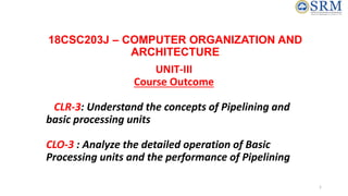
- 1. 18CSC203J – COMPUTER ORGANIZATION AND ARCHITECTURE UNIT-III Course Outcome CLR-3: Understand the concepts of Pipelining and basic processing units CLO-3 : Analyze the detailed operation of Basic Processing units and the performance of Pipelining 1
- 2. Topics Covered • Fundamental concepts of basic processing unit • Performing ALU operation • Register Transfer • Execution of complete instruction • Multiple bus organization • Hardwired control • Generation of control signals • Micro-programmed control, Microinstruction • Micro-program Sequencing • Micro instruction with Next address field 2
- 3. PROCESSING UNIT FUNCTIONS OF CPU: • CPU carries out all forms of data processing tasks. • It saves information, intermediate results and instructions. • CPU monitors the functionality of all computer components. COMPONENTS OF CPU: • Memory or storage unit: The memory unit stores all the instructions and data. This unit provides data to other units of the computer if necessary. Also known as main memory, or RAM (Random Access Memory). • Control unit: This unit monitors all computing processes but does not execute actual data processing. • Arithmetic Logic Unit (ALU): This does all the calculations and makes the decisions. 3
- 4. FUNDAMENTAL CONCEPTS OF BASIC PROCESSING UNIT • Processor fetches one instruction at a time and perform the specified operation. • Instructions are fetches from successive memory locations except for branch/ jump instruction. • The address of the next instruction to be executed is tracked by the Program Counter (PC) register. • Instruction Register (IR) contains instruction that is currently executed. • Instruction execution happens in three phases: Fetch: Fetch the instruction from the specified memory Decode: Determined the opcode and the operands Execute: Run the instruction 4
- 5. REGISTER TRANSFERS 5 • For each register two control signals are used : To place the contents of that register on the bus To load the data on the bus into register • The input and output of register are connected to the bus through switches controlled by the signals Rin and Rout.
- 6. SIGNAL DIAGRAM For Register Transfer 6
- 7. EXECUTING AN INSTRUCTION • Transfer a word of data from one processor register to another or to the ALU • Perform Arithmetic and Logic operation and store the result in processor register • Fetch the contents of a given memory location and load into processor register. • Store a word of data from a processor register into a given memory location • Fetch the contents of memory location pointed by the PC. The contents of this memory location is loaded to the IR-Fetch phase IR [[PC]] • Increment the PC by 4 (assume the word size as 4 ) PC[PC]+4 • Carry out the actions specified by the instruction in the IR-Execution phase • Datapath • MDR: Two inputs and two outputs since data can be loaded from memory or processor bus. • MAR: Input line is connected to internal bus and output line to external bus • Control lines: uses instruction decoder and control logic block to issue control signals • R0-R(n-1): General Purpose registers whose numbers vary between processors. • TEMP, Y and Z: Temporary registers used by the processor during instruction execution 7
- 8. 8 Fig : Single bus organization of datapath
- 9. EXECUTION OF COMPLETE INSTRUCTION • Initiate instruction fetch by loading contents of PC to MAR. • Send Read request to memory. Incrementing PC • Contents of PC is loaded to register B. • Set select signal to 4, which make multiplexer to select const 4, which is then added to B. The result is available in Z. • The content of Z is loaded to PC. Load IR • The word is fetched from the memory and loaded into IR • Decoding: Instruction decoding circuit interprets contents of IR. • Execution: Control circuitry is activated to issue relevant control signals. • Load MAR with contents of R3. Initiate memory read. Transfer R1 to Y. ADD (R3), R1 • Perform addition on Y and MDR after selecting Y. • Load the result from Z to R1. 9
- 10. PERFORMING AN ARITHMETIC OR LOGIC OPERATION • The ALU is a combinational circuit that has no internal storage. • ALU gets the two operands from MUX and bus. The result is temporarily stored in register Z. • The sequence of operations to add contents of R1 and R2 and store it in R3: FETCHING WORD FROM MEMORY • Address will be loaded into MAR from PC • Read operation will be issued in the bus and the data will be loaded into MDR. • Wait for Memory Function Completed (WMFC): This signal is issued to make the processor to wait for the reply from the memory (MFC ). Fig: Fetching word form Memory 10
- 11. EXECUTION OF BRANCH INSTRUCTIONS • Branch instruction replaces the contents of PC with the branch target address, which is usually obtained by adding an offset X given in the branch instruction. • The offset X is usually the difference between the branch target address and the address immediately following the branch instruction. • Two types of branch: conditional and unconditional branch Unconditional Branch: • Offset value : branch target address –address immediately following the branch instruction. • Offset value is obtained from IR and is available in X. • Y contains the updated PC value. Add the offset address along with PC to find the branch target. • Now load the calculated branch target from Z to PC. 11
- 12. • Check status of condition codes before loading branch target into PC Condition Codes • The CPU maintains a set of single-bit condition code registers. • These registers are set by arithmetic and logical operations and can be tested to perform conditional branches. Examples: Carry flag. If set, the most recent operation generated a carry out of the most significant bit. Use to detect overflow for unsigned operations. Zero flag. The most recent operation yielded zero. Sign flag. The most recent operation yielded a negative value. Overflow flag. The most recent operation caused a two’s complement overflow – either negative or positive. Branch on negative • If N=0 then the processor return to step 1 after step 4. • If N=1 then load a new value into PC to perform branching. EXECUTION OF CONDITIONAL BRANCH 12
- 13. MULTIPLE BUS ORGANIZATION • Single bus structure takes long time for transfer of data in a clock cycle • To avoid the above said process ,multiple internal paths are enabled in commercial processors . • This allows to have several transfers to take place in parallel 13
- 14. Multi Bus • The next slide has the three bus structure which is connecting registers and the ALU of processors • Register file: is a single block of all general purpose registers • Register file has three ports. • First Two output ports are connected to different registers placed on the Bus A and Bus B. • One more third port connected to Bus C during the same clock cycle. • Buses A and B used to Transfer the source operands to A and B inputs of ALU.(Arithmetic and logic operations are performed) • The result is transferred over the Bus C. • Three bus arrangement avoids the usage of registers Y and Z. • Incrementer Unit: is used to increment the PC by 4 which eliminates the usage of ALU. 14
- 15. Cont… • It increments the other addresses such as the memory addresses in Load and Store Multiple instructions. • Three operand instruction • Add R4,R5,R6 • STEP1: The contents of the PC are passed through the ALU using R=B control signal and loaded into MAR for(Memory Read operation) and the PC is incremented by 4 • Step2: The processor waits for MFC (WMFC-Wait for Memory Function completed) • STEP3: MFC loads the data received into MDR. And again data is transferred into IR • STEP4: Final execution phase requires only one control step providing more paths for data transfer results in reduction of clock cycles needed to execute an instruction. 15
- 17. Multiple-Bus Organization • Add R4, R5, R6 Step Action 1 PCout , R=B, MARin , Read, IncPC 2 WMFC 3 MDRoutB , R=B, IRin 4 R4outA , R5 outB , SelectA, Add, R6in , End Figure 7.9. Control sequence for the instruction. Add R4,R5,R6, for the three-bus organization in Figure 7.8. 17
- 19. Overview • To execute instructions, the processor must have some means of generating the control signals needed in the proper sequence. • Two categories: hardwired control and microprogrammed control • Hardwired system can operate at high speed; but with little flexibility. 19
- 20. Step Action 1 PCout , MARin , Read, Select4, Add, Zin 2 Zout , PCin , Yin , WMF C 3 MDRout , IRin 4 R3out , MARin , Read 5 R1out , Yin , WMF C 6 MDRout , SelectY,Add, Zin 7 Zout , R1in , End Figure 7.6. Control sequence for executionof the instruction Add (R3),R1. 7 Steps: 20
- 21. Cont… • The before slide depicts the sequence of control signals • Every step is completed in one clock period • Counter is used to keep track of the control steps. • Control signals are determined by following information 1. Contents of the control step counter 2. Contents of instruction register 3. Contents of condition code flags 4. External input signals, such as MFC and interrupt requests 21
- 22. Decoder/encoder block • Is a combinational circuit that generates the required control outputs depending on the state of all its input. • The control unit organization of the decoder and encoder block is shown in the next slide 22
- 23. Control Unit Organization Figure 7.10. Control unit organization. CLK Clock Control step IR encoder Decoder/ Control signals codes counter inputs Condition External 23
- 24. Detailed Block Description External inputs Figure 7.11. Separation of the decoding and encoding functions. Encoder Reset CLK Clock Control signals counter Run End Condition codes decoder Instruction Step decoder Control step IR T1 T2 Tn INS1 INS2 INS m 24
- 25. Explanation of decoding and encoding • The step decoder provides a separate signal signal line for each step or time slot in the control sequence • Output of the instruction decoder consists of separate line for each machine instruction. • Any instruction loaded into IR,one of the output lines INS1 trough INSm is set to 1 and all others are set to 0. • The input signals to the encoder are combined to generate individual control signals Yin,PCout 25
- 26. Generating Zin • Zin = T1 + T6 • ADD + T4 • BR + … • The signal is asserted during time slot T1 for all instruction ,T6 for an ADD instruction ,T4 for unconditional branch instruction Figure 7.12. Generation of the Zin control signal for the processor in Figure 7.1. T 1 Add Branch T 4 T 6 26
- 27. Generating End • End = T7 • ADD + T5 • BR + (T5 • N + T4 • N) • BRN +… Figure 7.13. Generation of the End control signal. T7 Add Branch Branch<0 T5 End N N T4 T5 27
- 28. End signal • End signRal starts a new instruction fetch cycle by resetting the control step counter to its starting value. • Control signal called RUN. • RUN set as 1 ,causes the counter to be incremented by one at the end of every clock cycle. • RUN equal to 0 , the counter stops counting • WMFC signal is issued to cause the processor to wait for the reply from memory 28
- 29. Cont… • These control unit organization viewed as state machine(one state to another in every clock cycle) • Output of the state machines are control signals. • Sequence of operations carried out by machine is determined by the wiring of logic elements,hence the name “hardwired”. • Controller operates at high speed 29
- 30. Complete Processor • This structure has instruction unit that fetches from instruction cache or from the main memory. • Processing unit to handle integer and floating point data. • Data cache is introduced between these units and main memory • Separate cache for instruction and data • Processor is connected to system bus. • Bus interface is used to connect to rest of memory and input output unit. 30
- 32. A control unit whose binary control variables are stored in memory is called a micro programmed control unit. Microprogrammed Control 32
- 33. 33 Microprogrammed Control Unit • Control signals • Group of bits used to select paths in multiplexers, decoders, arithmetic logic units • Control variables • Binary variables specify microoperations • Certain microoperations initiated while others idle • Control word • String of 1’s and 0’s represent control variables
- 34. 34 Microprogrammed Control Unit • Control memory • Memory contains control words • Microinstructions • Control words stored in control memory • Specify control signals for execution of microoperations • Microprogram • Sequence of microinstructions
- 35. 35 Control Unit Implementation • Hardwired • Micro programmed Instruction code Combinational Logic Circuits Memory Sequence Counter . . Control signals Control signals Next Address Generator (sequencer) CA R Control Memory CDR Decoding Circuit Memory . . CAR: Control Address Register CDR: Control Data Register Instruction code
- 36. 36 Control Memory • Read-only memory (ROM) • Content of word in ROM at given address specifies microinstruction • Each computer instruction initiates series of microinstructions (microprogram) in control memory • These microinstructions generate microoperations to • Fetch instruction from main memory • Evaluate effective address • Execute operation specified by instruction • Return control to fetch phase for next instruction Control memory (ROM) Control word (microinstruction) Address
- 37. 37 • Control memory • Contains microprograms (set of microinstructions) • Microinstruction contains • Bits initiate microoperations • Bits determine address of next microinstruction • Control address register (CAR) • Specifies address of next microinstruction Micro programmed Control Organization Control word Next Address Generator (sequencer) CA R Control Memory (ROM) CDR External input
- 38. 38 Microprogrammed Control Organization • Next address generator (microprogram sequencer) • Determines address sequence for control memory • Microprogram sequencer functions • Increment CAR by one • Transfer external address into CAR • Load initial address into CAR to start control operations
- 39. 39 Microprogrammed Control Organization • Control data register (CDR)- or pipeline register • Holds microinstruction read from control memory • Allows execution of microoperations specified by control word simultaneously with generation of next microinstruction • Control unit can operate without CDR Control word Next Address Generator (sequencer) CA R Control Memory (ROM) External input
- 40. Microinstruction Sequencing: A micro-program control unit can be viewed as consisting of two parts: The control memory that stores the microinstructions. Sequencing circuit that controls the generation of the next address. 40
- 41. Microinstruction Sequencing: A micro-program sequencer attached to a control memory inputs certain bits of the microinstruction, from which it determines the next address for control memory. A typical sequencer provides the following address- sequencing capabilities: Increment the present address for control memory. Branches to an address as specified by the address field of the micro instruction. Branches to a given address if a specified status bit is equal to 1. Transfer control to a new address as specified by an external source (Instruction Register). Has a facility for subroutine calls and returns. 41
- 42. Microinstruction Sequencing: Depending on the current microinstruction condition flags, and the contents of the instruction register, a control memory address must be generated for the next micro instruction. There are three general techniques based on the format of the address information in the microinstruction: Two Address Field. Single Address Field. Variable Format 42
- 43. Two address field The simplest approach is to provide two address field in each microinstruction and multiplexer is provided to select: Address from the second address field. Starting address based on the OPcode field in the current instruction. The address selection signals are provided by a branch logic module whose input consists of control unit flags plus bits from the control partition of the micro instruction. 43
- 45. Single address field Two-address approach is simple but it requires more bits in the microinstruction. With a simpler approach, we can have a single address field in the micro instruction with the following options for the next address. Address Field. Based on OPcode in instruction register. Next Sequential Address. enter image description here The address selection signals determine which option is selected. This approach reduces the number of address field to one. In most cases (in case of sequential execution) the address field will not be used. Thus the microinstruction encoding does not efficiently utilize the entire microinstruction. 45
- 47. Variable Format In this approach, there are two entirely different microinstruction formats. One bit designates which format is being used. In this first format, the remaining bits are used to activate control signals. In the second format, some bits drive the branch logic module, and the remaining bits provide the address. With the first format, the next address is either the next sequential address or an address derived from the instruction register. With the second format, either a conditional or unconditional branch is specified. 47
- 49. 49 Address Sequencing • Address sequencing capabilities required in control unit • Incrementing CAR • Unconditional or conditional branch, depending on status bit conditions • Mapping from bits of instruction to address for control memory • Facility for subroutine call and return
- 50. 50 Address Sequencing Instruction code Mapping logic Multiplexers Control memory (ROM) Subroutine Register (SBR) Branch logic Status bits Microoperations Control Address Register (CAR) Incrementer MUX select select a status bit Branch address
- 51. 51 Microprogram Example Computer Configuration MUX AR 10 0 PC 10 0 Address Memory 2048 x 16 MUX DR 15 0 Arithmetic logic and shift unit AC 15 0 SBR 6 0 CAR 6 0 Control memory 128 x 20 Control unit
- 52. 52 Microprogram Example Microinstruction Format EA is the effective address Symbol OP-code Description ADD 0000 AC AC + M[EA] BRANCH 0001 if (AC < 0) then (PC EA) STORE 0010 M[EA] AC EXCHANGE 0011 AC M[EA], M[EA] AC Computer instruction format I Opcode 15 14 11 10 Address 0 Four computer instructions F1 F2 F3 CD BR AD 3 3 3 2 2 7 F1, F2, F3: Microoperation fields CD: Condition for branching BR: Branch field AD: Address field
- 53. 53 Microinstruction Fields F1 Microoperation Symbol 000 None NOP 001 AC AC + DR ADD 010 AC 0 CLRAC 011 AC AC + 1 INCAC 100 AC DR DRTAC 101 AR DR(0-10) DRTAR 110 AR PC PCTAR 111 M[AR] DR WRITE F2 Microoperation Symbol 000 None NOP 001 AC AC - DR SUB 010 AC AC DR OR 011 AC AC DR AND 100 DR M[AR] READ 101 DR AC ACTDR 110 DR DR + 1 INCDR 111 DR(0-10) PC PCTDR F3 Microoperation Symbol 000 None NOP 001 AC AC DR XOR 010 AC AC’ COM 011 AC shl AC SHL 100 AC shr AC SHR 101 PC PC + 1 INCPC 110 PC AR ARTPC 111 Reserved
- 54. 54 Microinstruction Fields CD Condition Symbol Comments 00 Always = 1 U Unconditional branch 01 DR(15) I Indirect address bit 10 AC(15) S Sign bit of AC 11 AC = 0 Z Zero value in AC BR Symbol Function 00 JMP CAR AD if condition = 1 CAR CAR + 1 if condition = 0 01 CALL CAR AD, SBR CAR + 1 if condition = 1 CAR CAR + 1 if condition = 0 10 RET CAR SBR (Return from subroutine) 11 MAP CAR(2-5) DR(11-14), CAR(0,1,6) 0
- 55. 55 Symbolic Microinstruction Sample Format Label: Micro-ops CD BR AD Label may be empty or may specify symbolic address terminated with colon Micro-ops consists of 1, 2, or 3 symbols separated by commas CD one of {U, I, S, Z} U: Unconditional Branch I: Indirect address bit S: Sign of AC Z: Zero value in AC BR one of {JMP, CALL, RET, MAP} AD one of {Symbolic address, NEXT, empty}
- 56. 56 Fetch Routine Fetch routine - Read instruction from memory - Decode instruction and update PC AR PC DR M[AR], PC PC + 1 AR DR(0-10), CAR(2-5) DR(11-14), CAR(0,1,6) 0 Symbolic microprogram for fetch routine: ORG 64 PCTAR U JMP NEXT READ, INCPC U JMP NEXT DRTAR U MAP FETCH: Binary microporgram for fetch routine: 1000000 110 000 000 00 00 1000001 1000001 000 100 101 00 00 1000010 1000010 101 000 000 00 11 0000000 Binary address F1 F2 F3 CD BR AD Microinstructions for fetch routine:
- 57. 57 Symbolic Microprogram • Control memory: 128 20-bit words • First 64 words: Routines for 16 machine instructions • Last 64 words: Used for other purpose (e.g., fetch routine and other subroutines) • Mapping: OP-code XXXX into 0XXXX00, first address for 16 routines are 0(0 0000 00), 4(0 0001 00), 8, 12, 16, 20, ..., 60 ORG 0 NOP READ ADD ORG 4 NOP NOP NOP ARTPC ORG 8 NOP ACTDR WRITE ORG 12 NOP READ ACTDR, DRTAC WRITE ORG 64 PCTAR READ, INCPC DRTAR READ DRTAR I U U S U I U I U U I U U U U U U U U CALL JMP JMP JMP JMP CALL JMP CALL JMP JMP CALL JMP JMP JMP JMP JMP MAP JMP RET INDRCT NEXT FETCH OVER FETCH INDRCT FETCH INDRCT NEXT FETCH INDRCT NEXT NEXT FETCH NEXT NEXT NEXT ADD: BRANCH: OVER: STORE: EXCHANGE: FETCH: INDRCT: Label Microops CD BR AD Partial Symbolic Microprogram
- 58. 58 Binary Micro program Address Binary Microinstruction Micro Routine Decimal Binary F1 F2 F3 CD BR AD ADD 0 0000000 000 000 000 01 01 1000011 1 0000001 000 100 000 00 00 0000010 2 0000010 001 000 000 00 00 1000000 3 0000011 000 000 000 00 00 1000000 BRANCH 4 0000100 000 000 000 10 00 0000110 5 0000101 000 000 000 00 00 1000000 6 0000110 000 000 000 01 01 1000011 7 0000111 000 000 110 00 00 1000000 STORE 8 0001000 000 000 000 01 01 1000011 9 0001001 000 101 000 00 00 0001010 10 0001010 111 000 000 00 00 1000000 11 0001011 000 000 000 00 00 1000000 EXCHANGE 12 0001100 000 000 000 01 01 1000011 13 0001101 001 000 000 00 00 0001110 14 0001110 100 101 000 00 00 0001111 15 0001111 111 000 000 00 00 1000000 FETCH 64 1000000 110 000 000 00 00 1000001 65 1000001 000 100 101 00 00 1000010 66 1000010 101 000 000 00 11 0000000 INDRCT 67 1000011 000 100 000 00 00 1000100 68 1000100 101 000 000 00 10 0000000
- 59. 59 Design of Control Unit microoperation fields 3 x 8 decoder 7 6 5 4 3 2 1 0 F1 3 x 8 decoder 7 6 5 4 3 2 1 0 F2 3 x 8 decoder 7 6 5 4 3 2 1 0 F3 Arithmetic logic and shift unit AND ADD DRTAC AC Load From PC From DR(0-10) Select 0 1 Multiplexers AR Load Clock AC DR DRTAR PCTAR
- 60. 60 Microprogram Sequencer 3 2 1 0 S1 MUX1 External (MAP) SBR Load Incrementer CAR Input logic I 0 T MUX2 Select 1 I S Z Test Clock Control memory Microops CD BR AD L I 1 S0 . . . . . .
- 61. 61 Input Logic for Microprogram Sequencer Input logic I0 I 1 T MUX2 Select 1 I S Z Test CD Field of CS From CPU BR field of CS L(load SBR with PC) for subroutine Call S0 S1 for next address selection I1I0T Meaning Source of Address S1S0 L 000 In-Line CAR+1 00 0 001 JMP CS(AD) 01 0 010 In-Line CAR+1 00 0 011 CALL CS(AD) and SBR <- CAR+1 01 1 10x RET SBR 10 0 11x MAP DR(11-14) 11 0 L S1 = I1 S0 = I0I1 + I1’T L = I1’I0T Input Logic
- 62. Address Sequencing Microinstructions are stored in control memory in groups, with each group specifying a routine. To appreciate the address sequencing in a micro-program control unit, let us specify the steps that the control must undergo during the execution of a single computer instruction. 62
- 63. Step-1 • An initial address is loaded into the control address register when power is turned on in the computer. • This address is usually the address of the first microinstruction that activates the instruction fetch routine. • The fetch routine may be sequenced by incrementing the control address register through the rest of its microinstructions. • At the end of the fetch routine, the instruction is in the instruction register of the computer. 63
- 64. Step-2 • The control memory next must go through the routine that determines the effective address of the operand. • A machine instruction may have bits that specify various addressing modes, such as indirect address and index registers. • The effective address computation routine in control memory can be reached through a branch microinstruction, which is conditioned on the status of the mode bits of the instruction. • When the effective address computation routine is completed, the address of the operand is available in the memory address register. 64
- 65. Step-3 • The next step is to generate the microoperations that execute the instruction fetched frommemory. • The microoperation steps to be generated in processor registers depend on the operation code part of the instruction. • Each instruction has its own micro-program routine stored in a given location of control memory. • The transformation from the instruction code bits to an address in control memory where the routine is located is referred to as a mapping process. • A mapping procedure is a rule that transforms the instruction code into a control memory address. 65
- 66. Step-4 • Once the required routine is reached, the microinstructions that execute the instruction may be sequenced by incrementing the control address register. • Micro-programs that employ subroutines will require an external register for storing the return address. • Return addresses cannot be stored in ROM because the unit has no writing capability. • When the execution of the instruction is completed, control must return to the fetch routine. • This is accomplished by executing an unconditional branch microinstruction to the first address of the fetch routine. 66