Downloaded 170 times
![Review of CMOS
image sensors
CHIN CHUN-CHIEH
[1] Y. HUO, C. C. FESENMAIER, AND P. B. CAT RYSSE, "MICROLENS PERFORMANCE
LIMITS IN SUB-2µM PIXEL CMOS IMAGE SENSORS," OPT . EXPRESS, VOL. 18, PP.
5861-5872, 2010.
[2] C. C. FESENMAIER, Y. HUO, AND P. B. CAT RYSSE, "O PT ICAL CONFINEMENT
METHODS FOR CONTINUEDSCALING OF CMOS IMAGE SENSOR PIXELS," OPT.
EXPRESS, VOL. 16, PP. 20457-20470, 2008.
[ 3 ] M . B I G A S , E . C A B R U J A , J . F O R E S T , A N D J . S A L V I , " R E V I EW O F C M O S I M A G E
SENSORS," MICROELECTRONICS JOURNAL, VOL. 37, PP. 433-451, 2006.
[4] S. KAVADIAS, B. DIERICKX, D. SCHEFFER, A. ALAERTS, D. UW AERTS, AND J.
BOGAERTS, "A LOGARITHMIC RESPONSE CMOS IMAGE SENSOR W ITH ON-CHIP
CALIBRATION," SOLID-STATE CIRCUITS, IEEE JOURNAL OF, VOL. 35, PP. 1146-
1152, 2000.
[5] S. MENDIS, S. E. KEMENY, AND E. R. FOSSUM, "CMOS ACTIVE PIXEL IMAGE
SENSOR," ELECTRON DEVICES, IEEE TRANSACTIONS ON, VOL. 41, PP. 452-
453, 1994.](https://image.slidesharecdn.com/reviewofcmosimagesensors-120707234155-phpapp01/75/Review-of-cmos-image-sensors-1-2048.jpg)
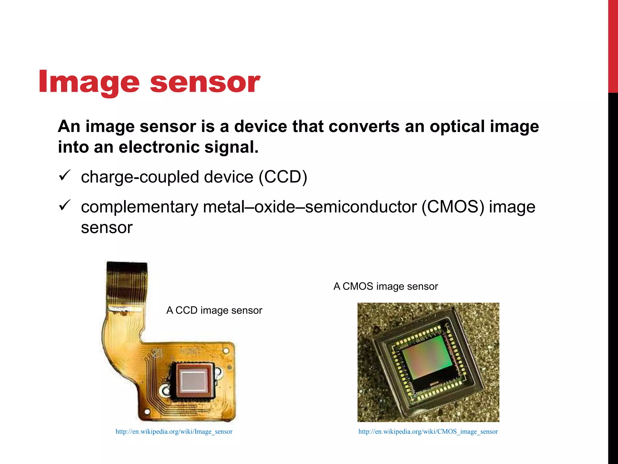
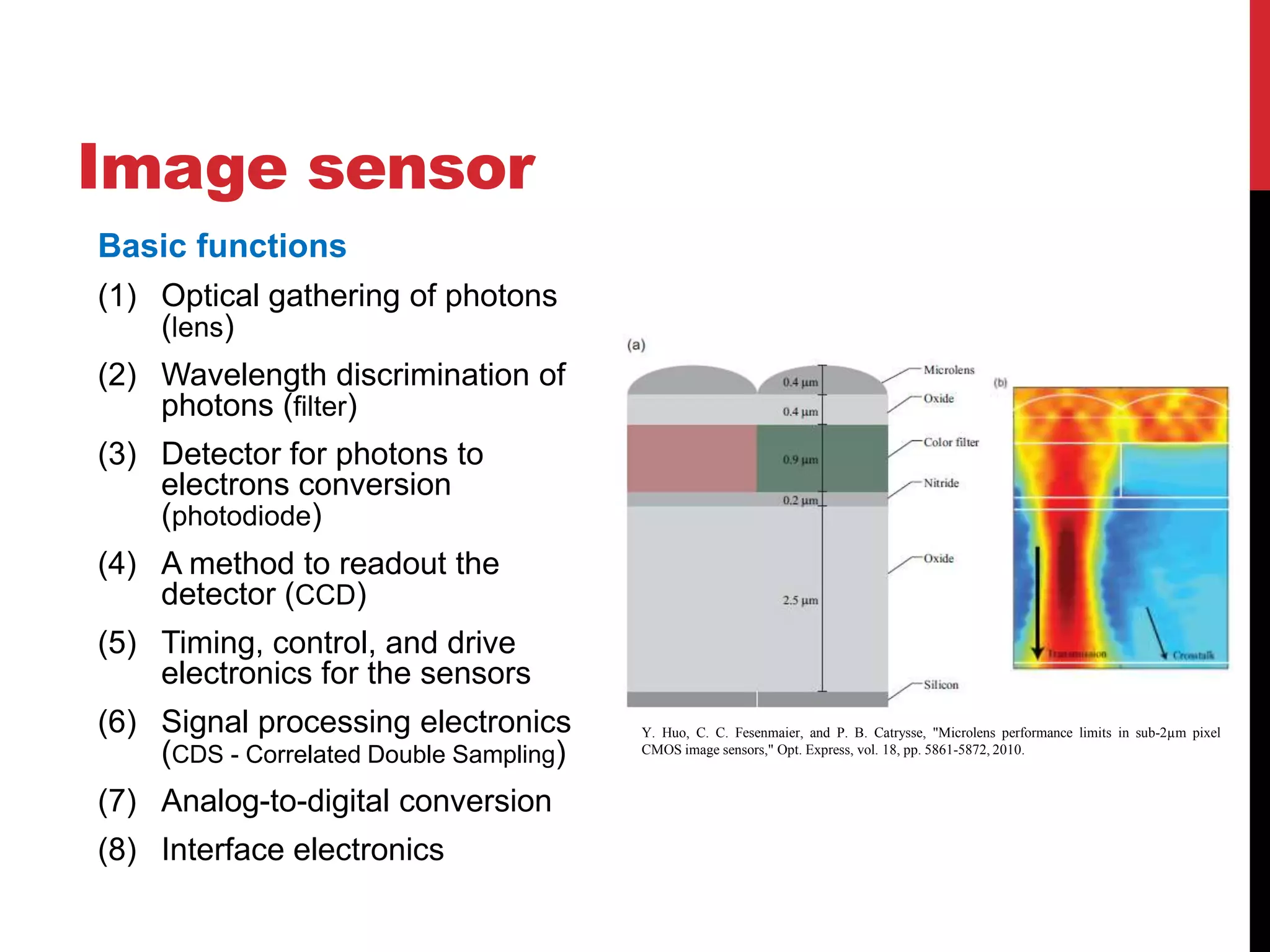
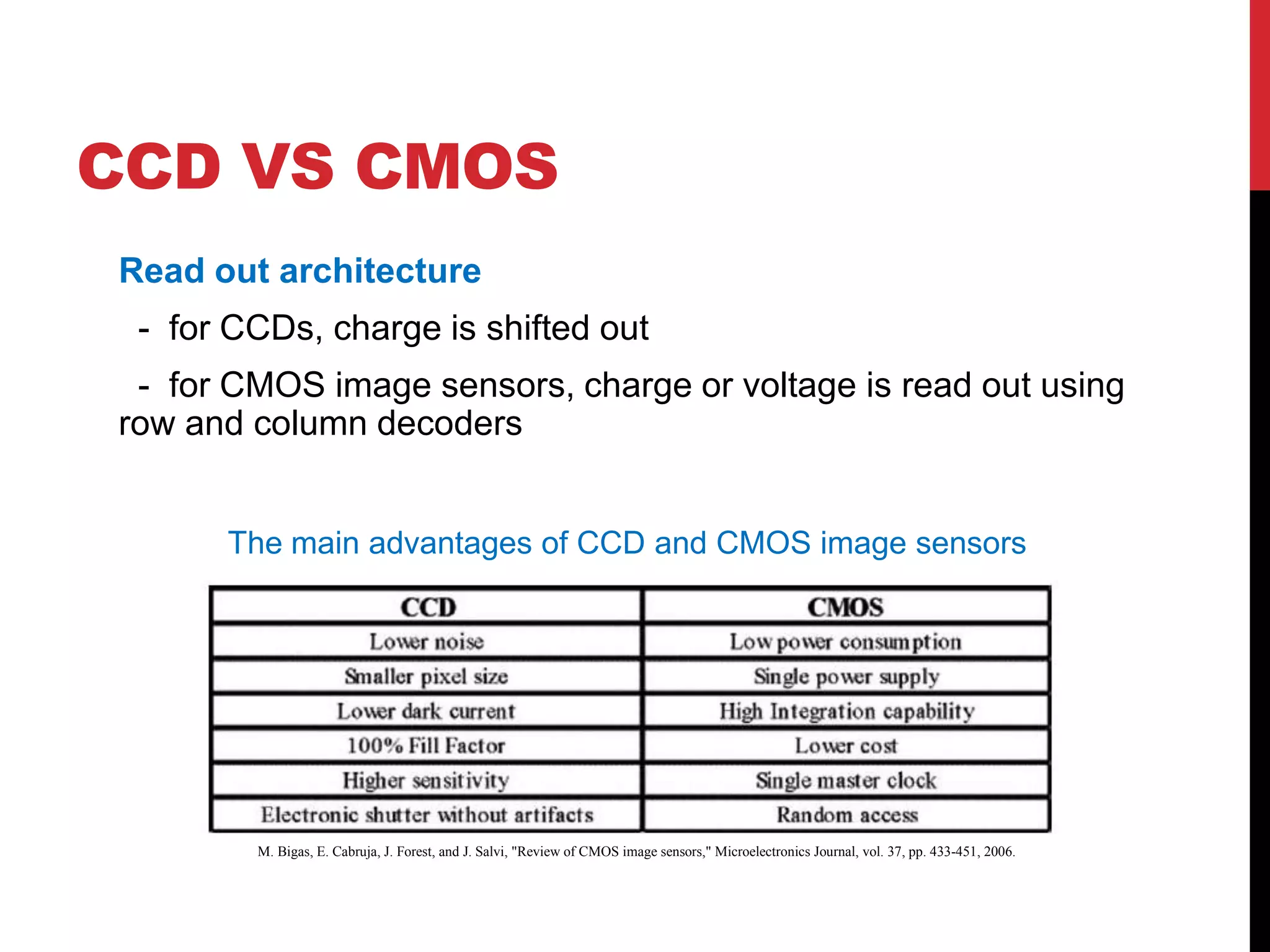
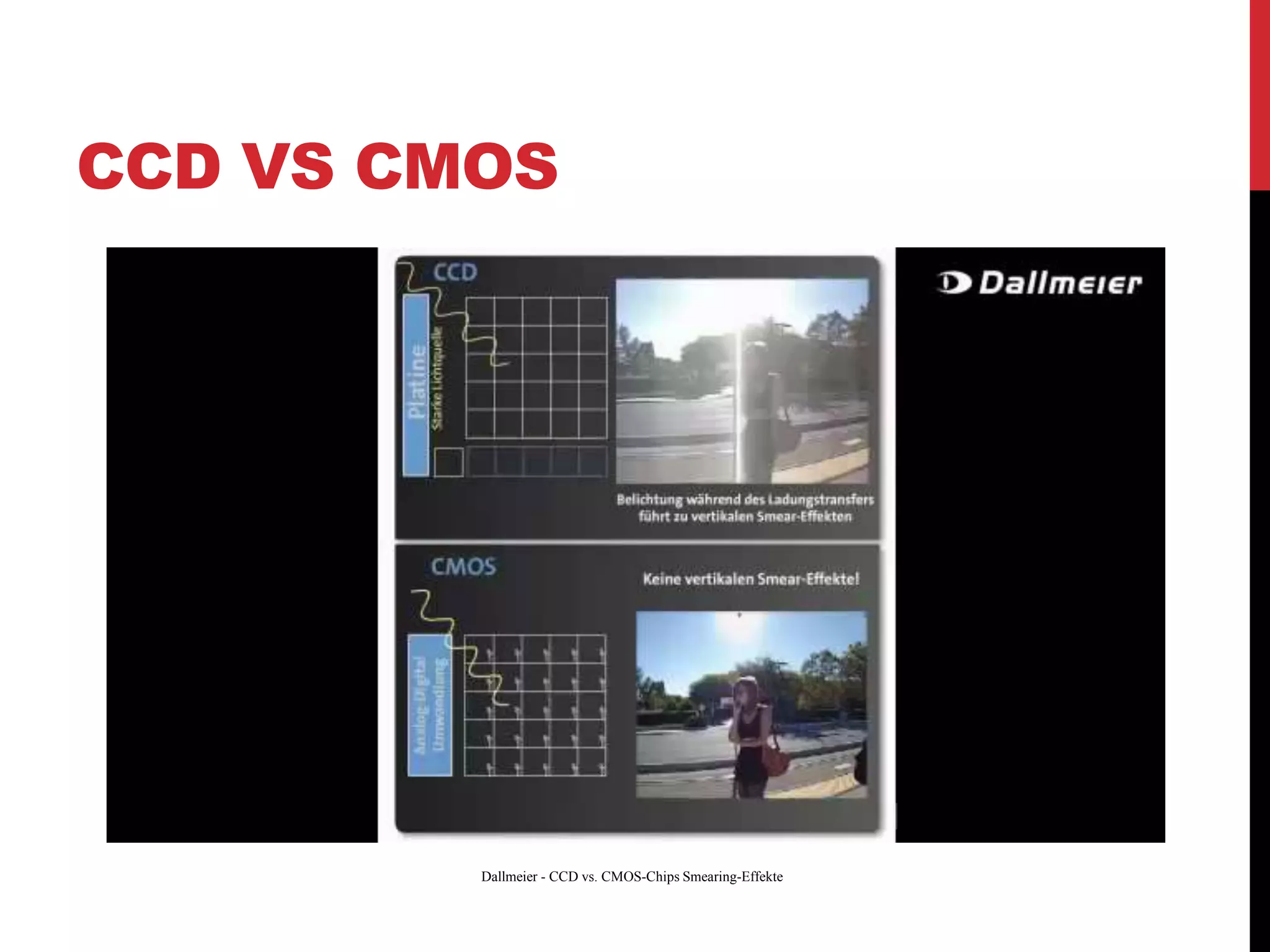
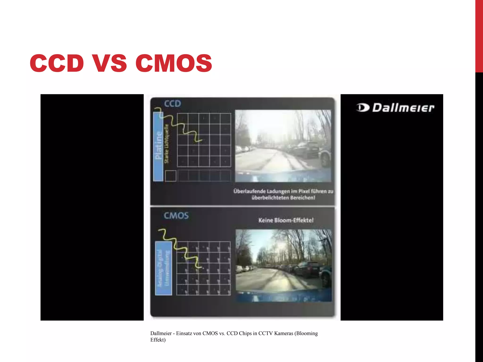
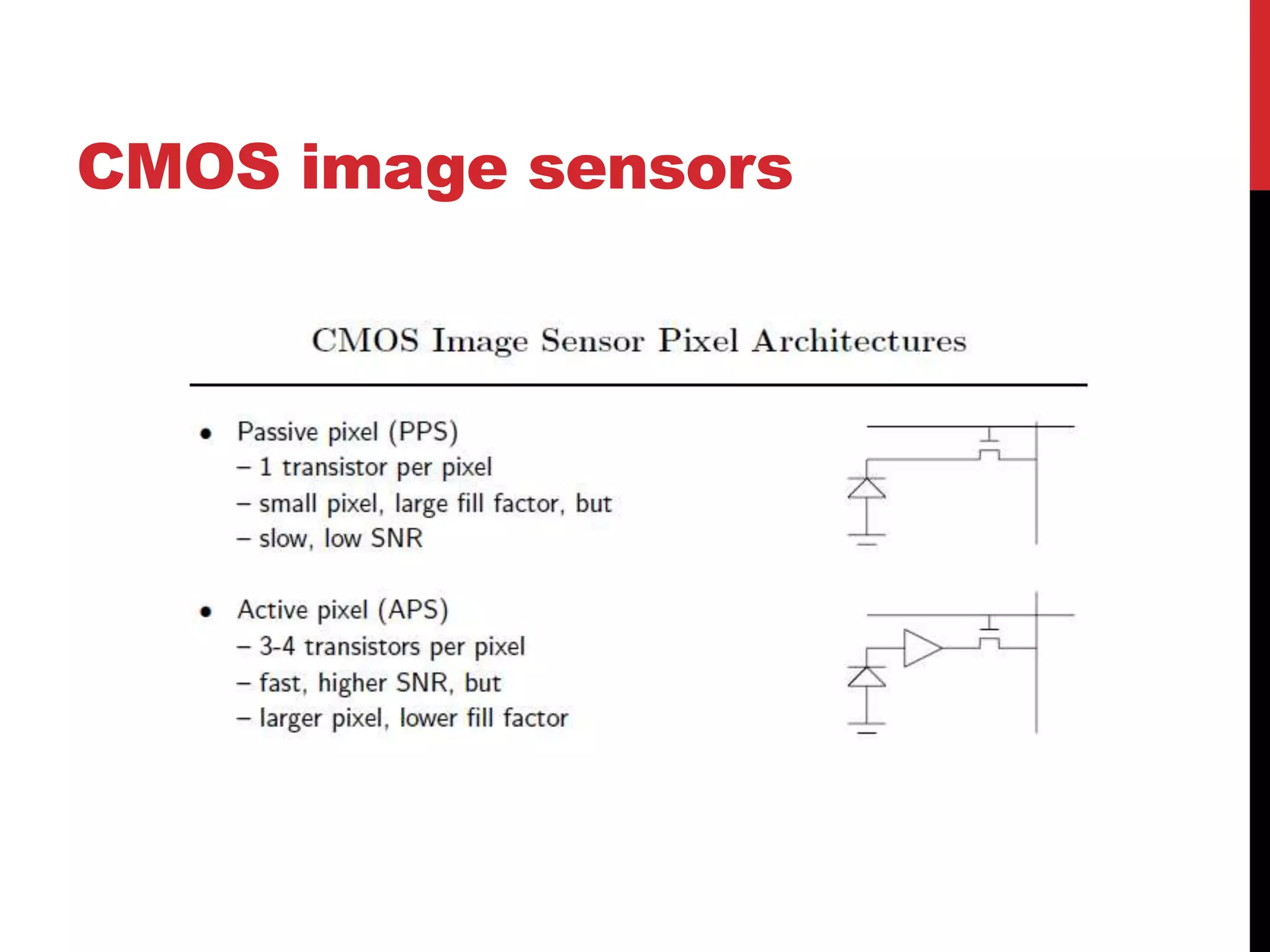
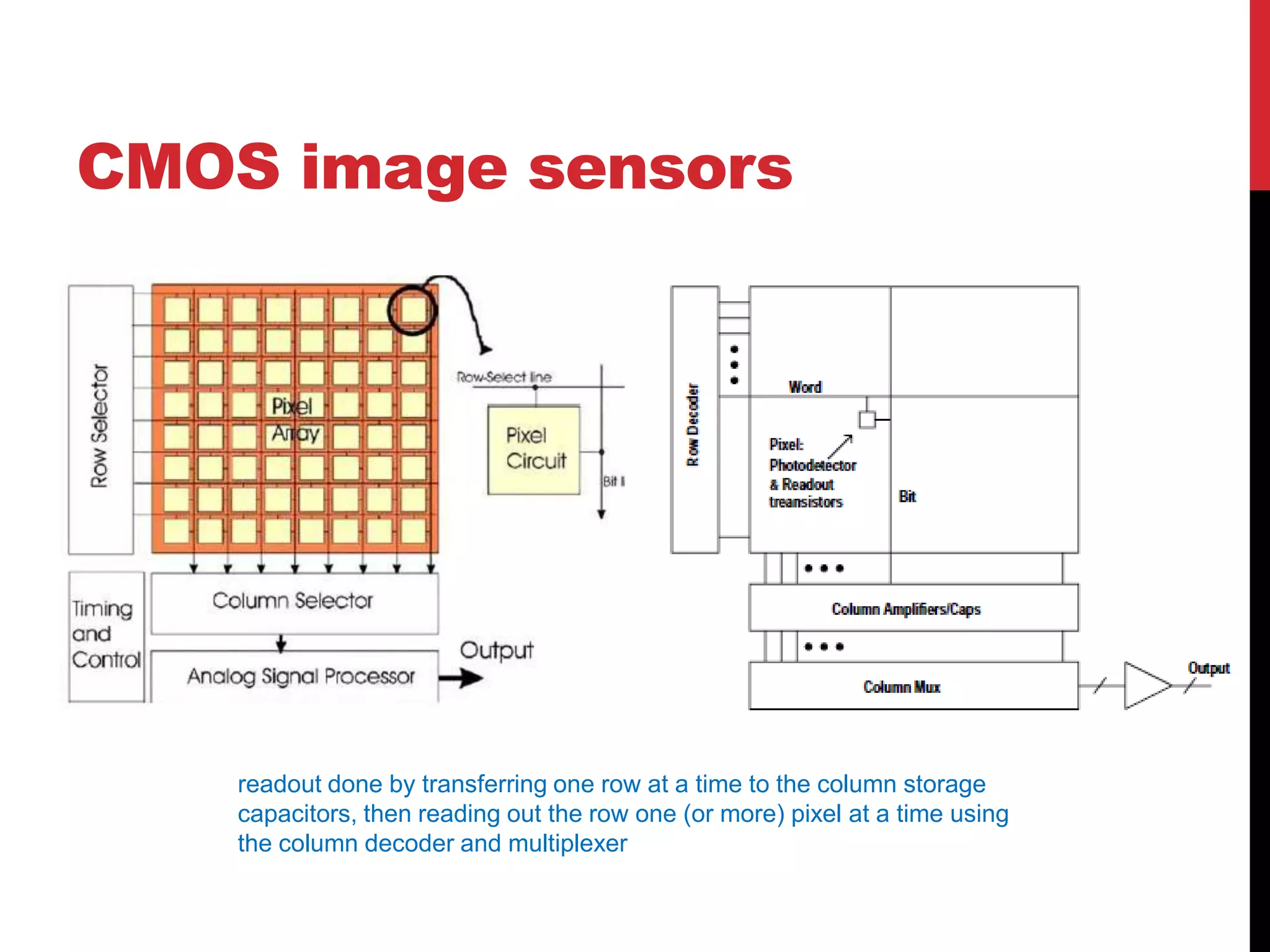
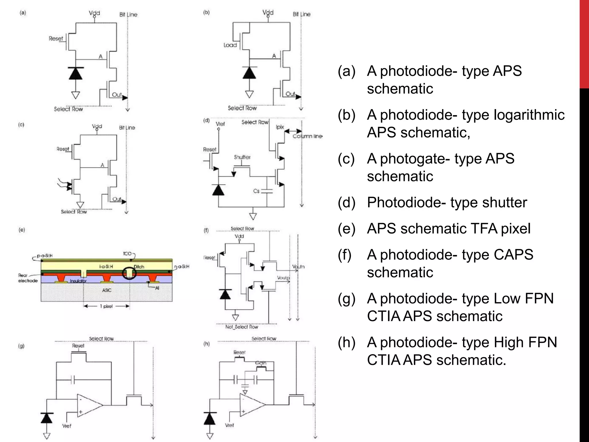

This document reviews CMOS image sensors. It discusses the basic functions of image sensors including light collection, wavelength discrimination, photon detection, readout methods, timing and control electronics, and signal processing. It compares CCD and CMOS image sensors, noting that CCDs shift charge out while CMOS sensors use row and column decoders to read out charge. The document outlines various figures of merit for image sensors such as noise, sensitivity, dynamic range, and speed. It also includes diagrams of CMOS image sensor pixel architectures.


![Vibe Coding vs. Spec-Driven Development [Free Meetup]](https://cdn.slidesharecdn.com/ss_thumbnails/vibecodingvsspecdrivendevelopment-251209105622-43f455e7-thumbnail.jpg?width=640&height=640&fit=bounds)


