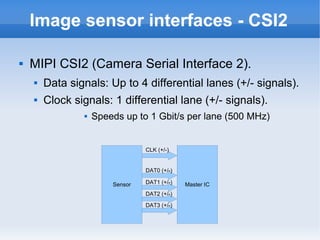
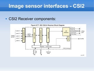
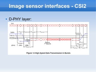
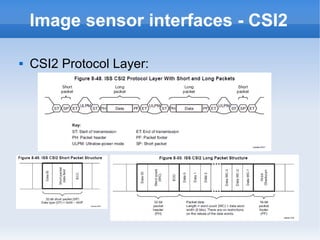
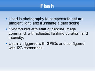
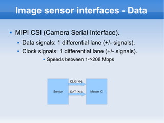
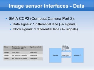
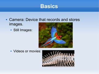
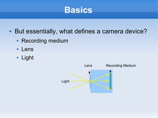
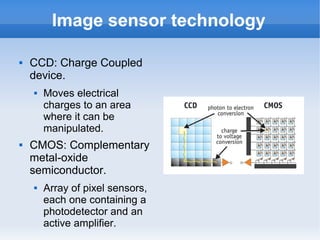
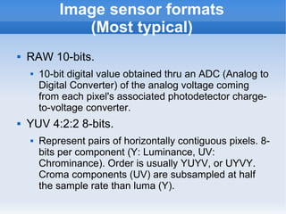
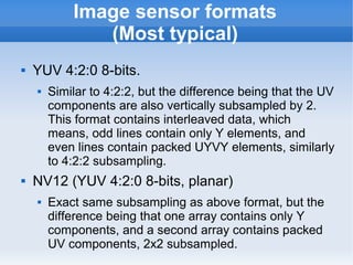
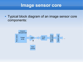
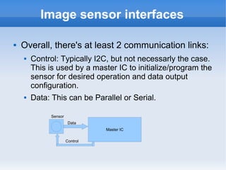
The document introduces cameras and their basic components. A typical digital camera contains an image sensor (CCD or CMOS), lens, flash, image signal processor, and storage media. Image sensors convert light into electrical signals using a grid of pixel sensors. Common image sensor formats are RAW, YUV 4:2:2, YUV 4:2:0, and NV12. The lens focuses light onto the image sensor. A camera communicates with peripherals using interfaces like I2C, parallel ports, CSI2, and SMIA CCP2.
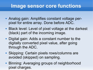
![Image sensor interfaces - Parallel
Parallel interface (a.k.a. Digital Video Port)
Data signals: 1 digital output pin per bit.
Sync signals:
PCLK: Pixel Clock.
HSYNC: Horizontal Sync.
VSYNC: Vertical Sync.
Horizontal Blanking
D[9:0]
Image data Sensor
PCLK
Master IC
HSYNC
VSYNC
Vertical Blanking](https://image.slidesharecdn.com/cameratrainingsergiopublic-120904235733-phpapp02/85/Camera-training-by-Sergio-Aguirre-15-320.jpg)