Downloaded 3,414 times
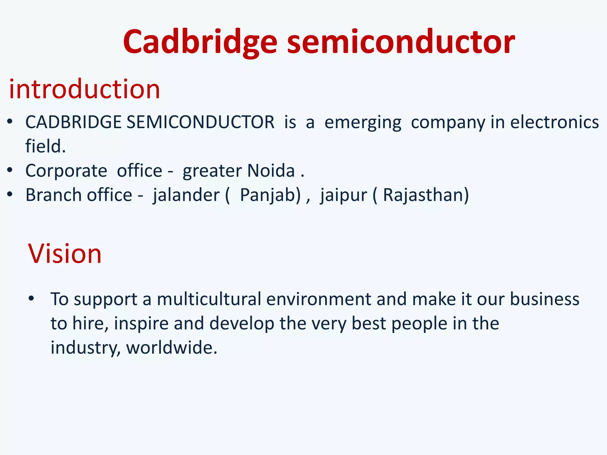
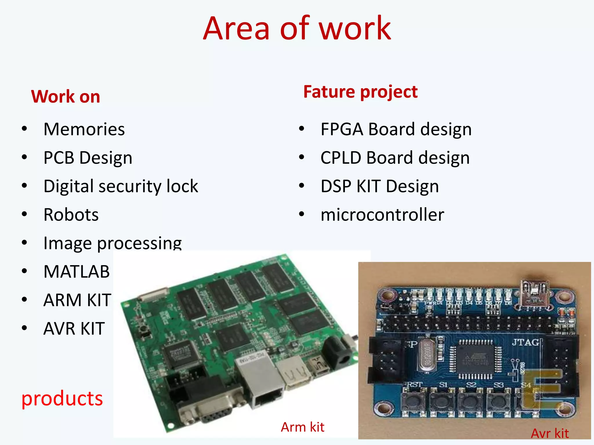
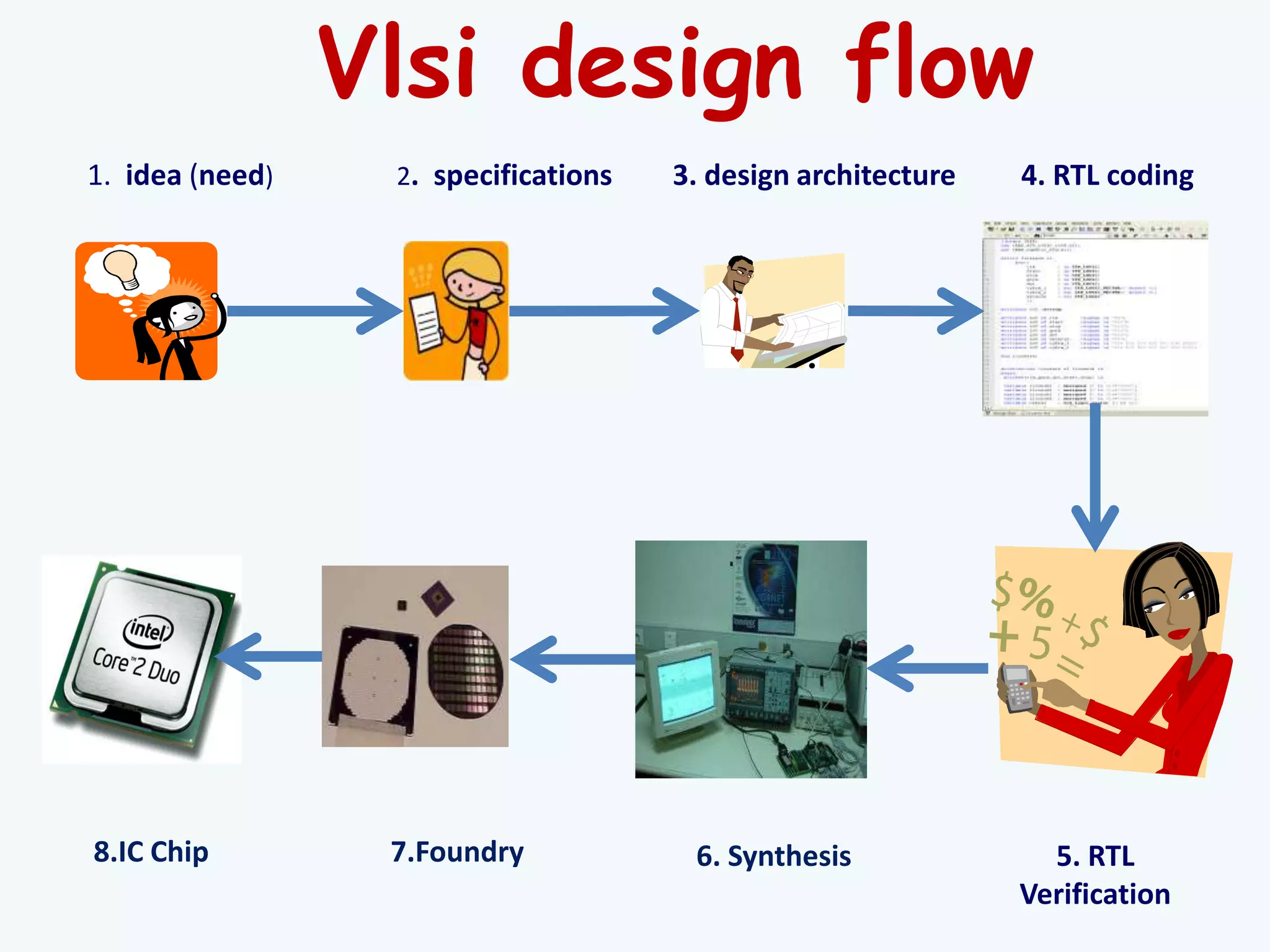
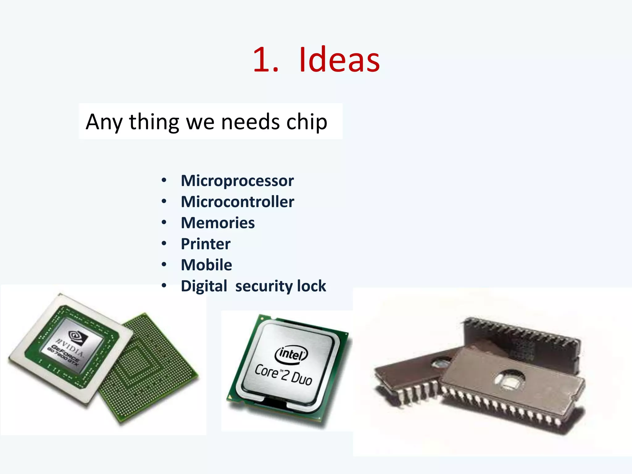
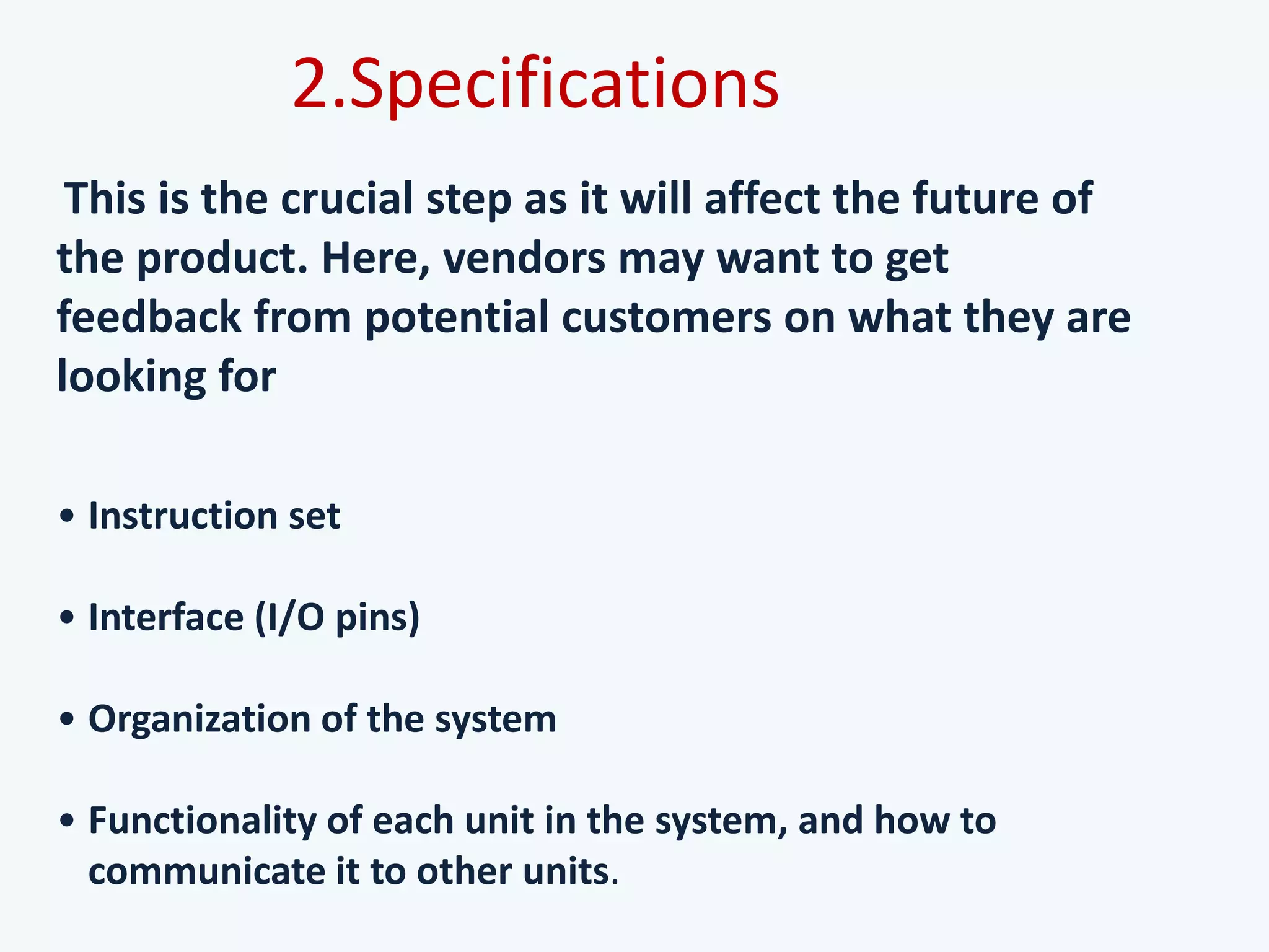
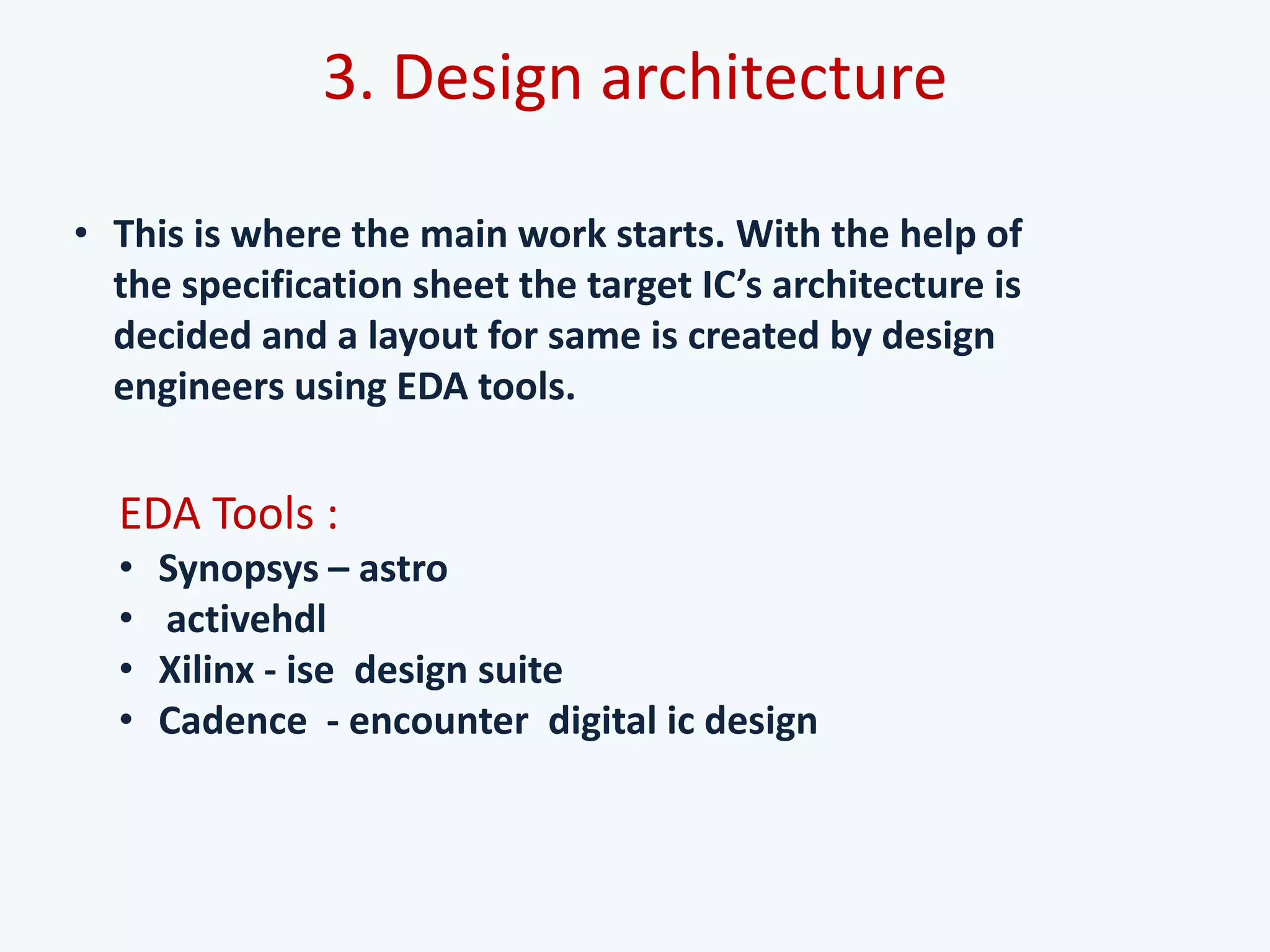
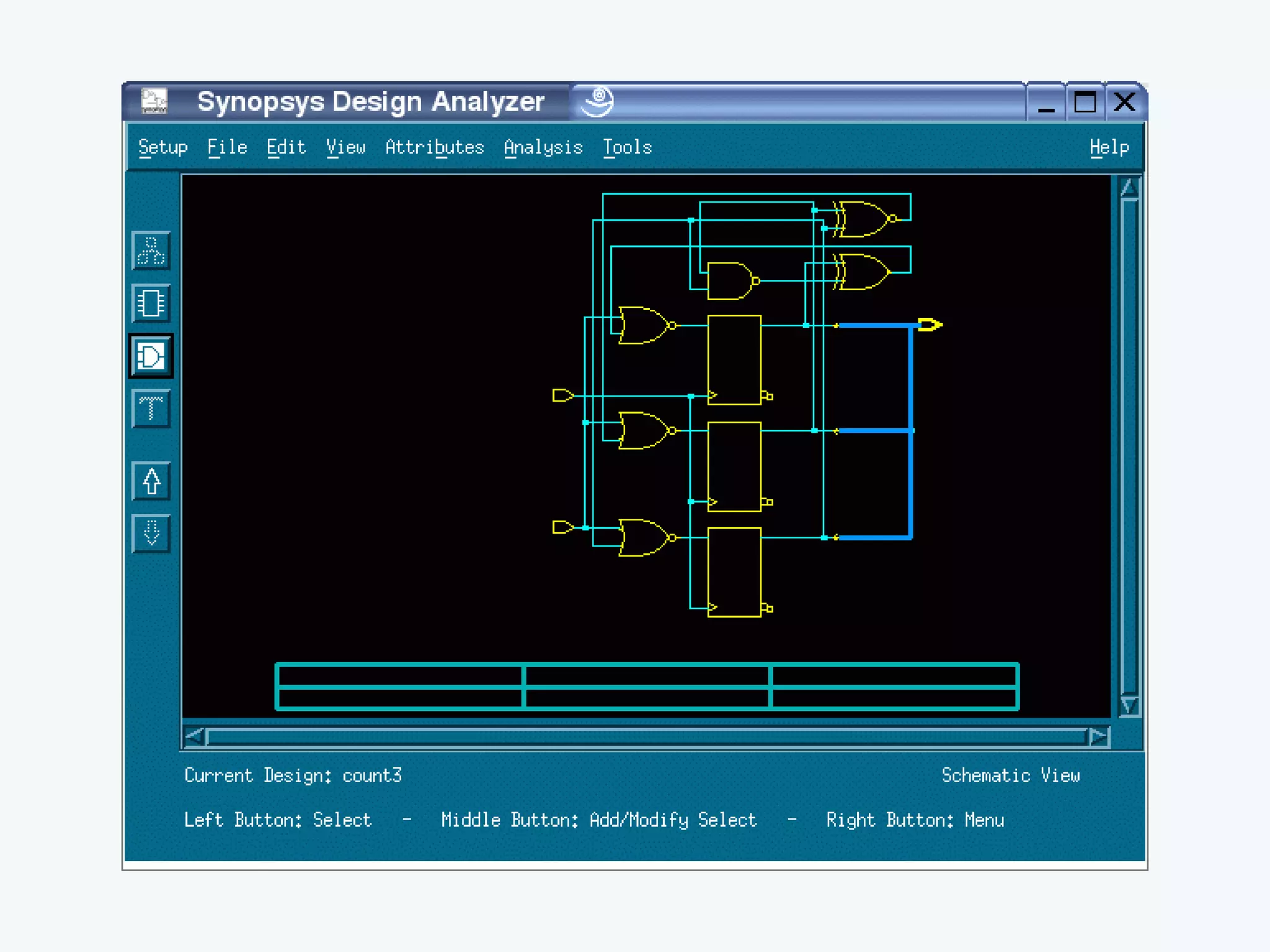

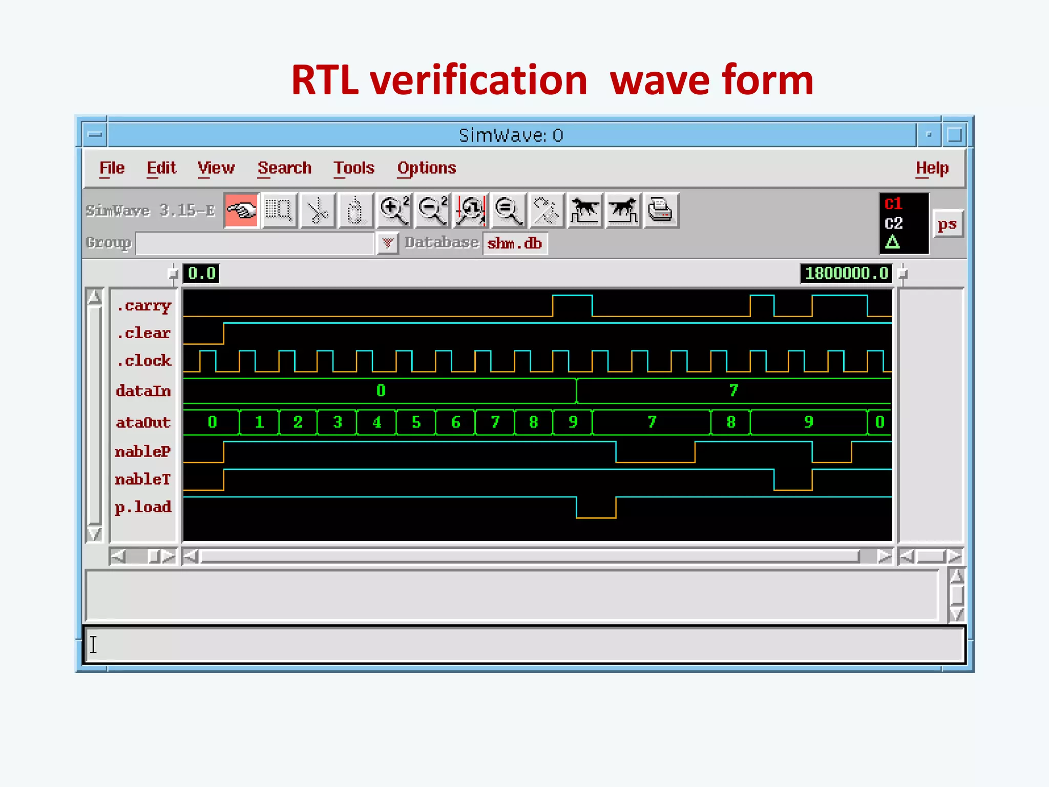
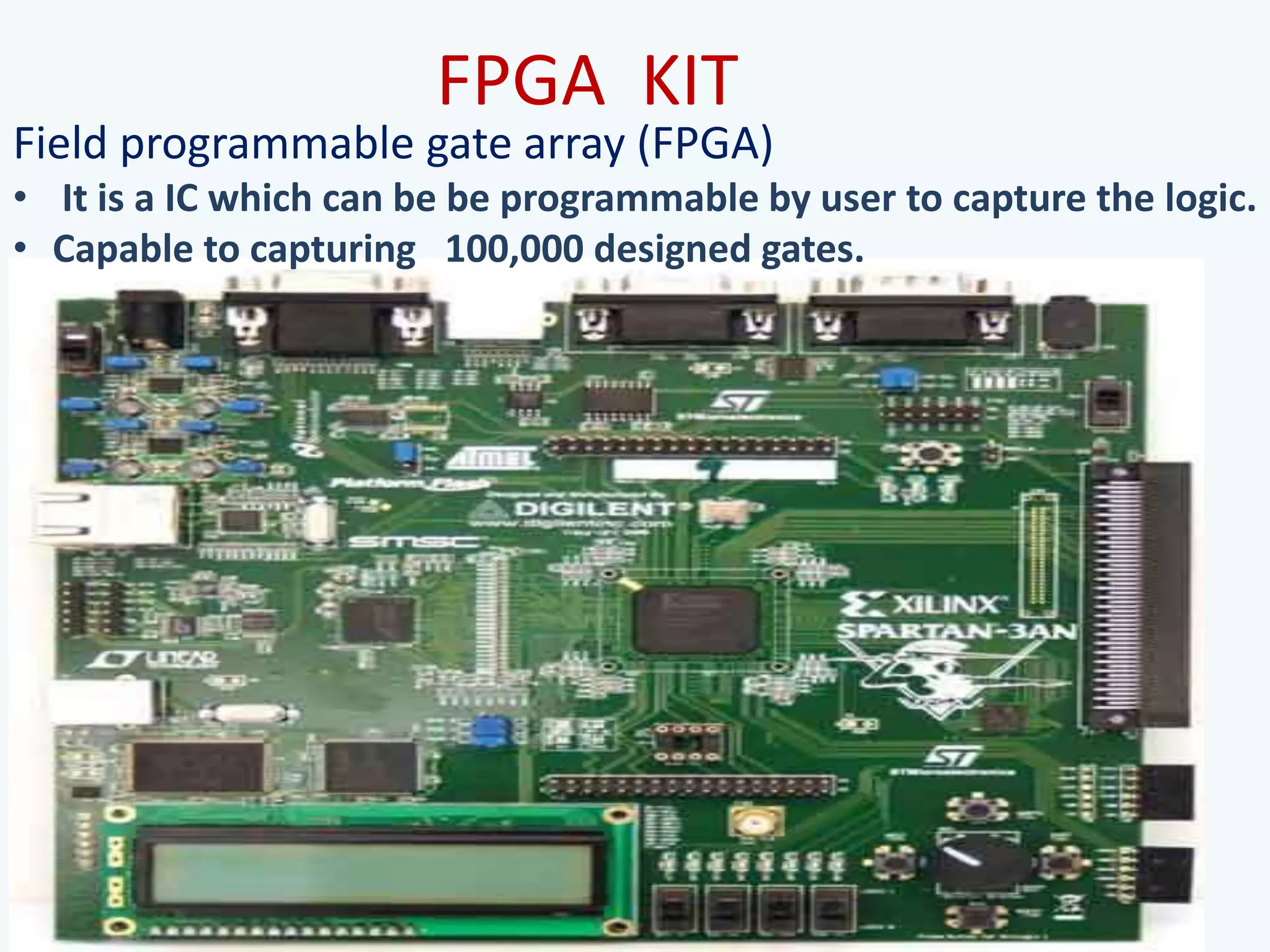
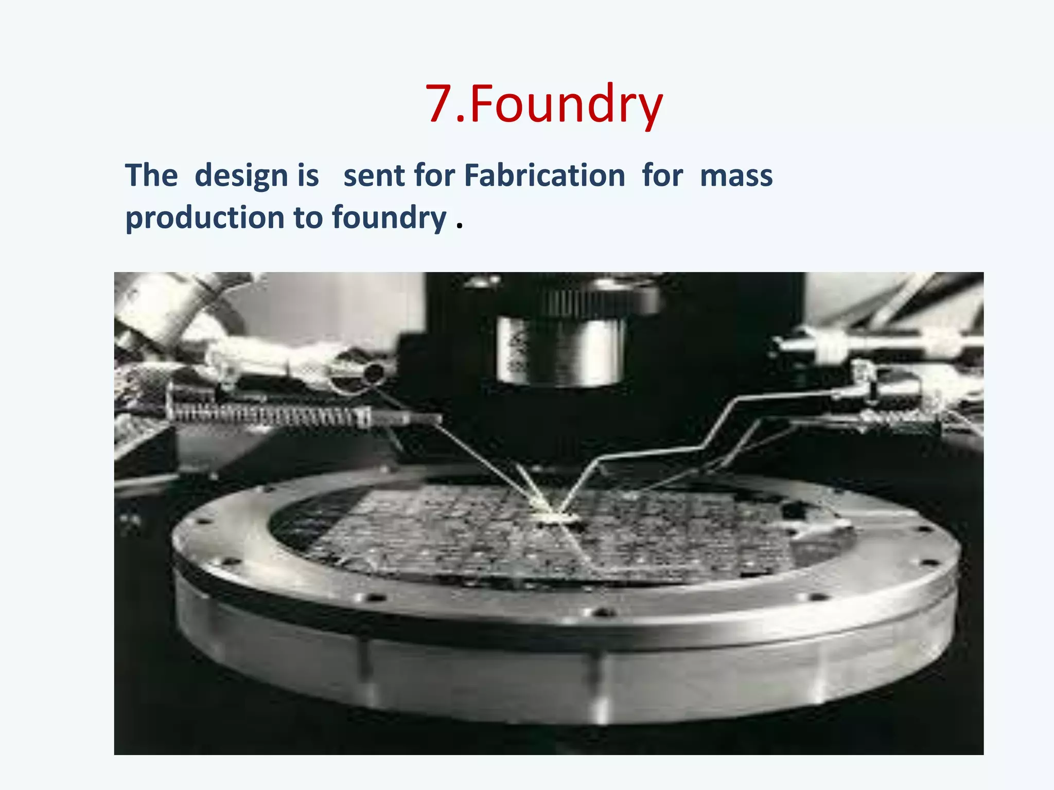
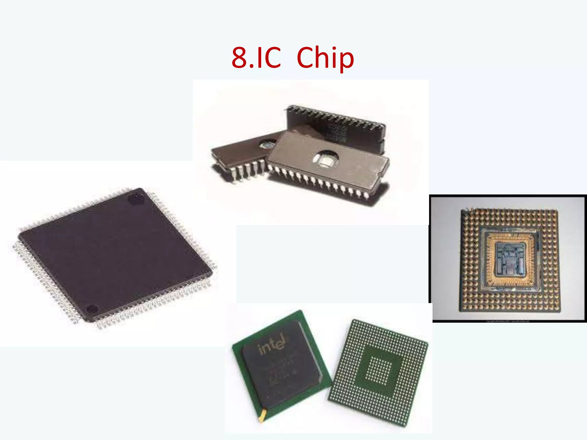
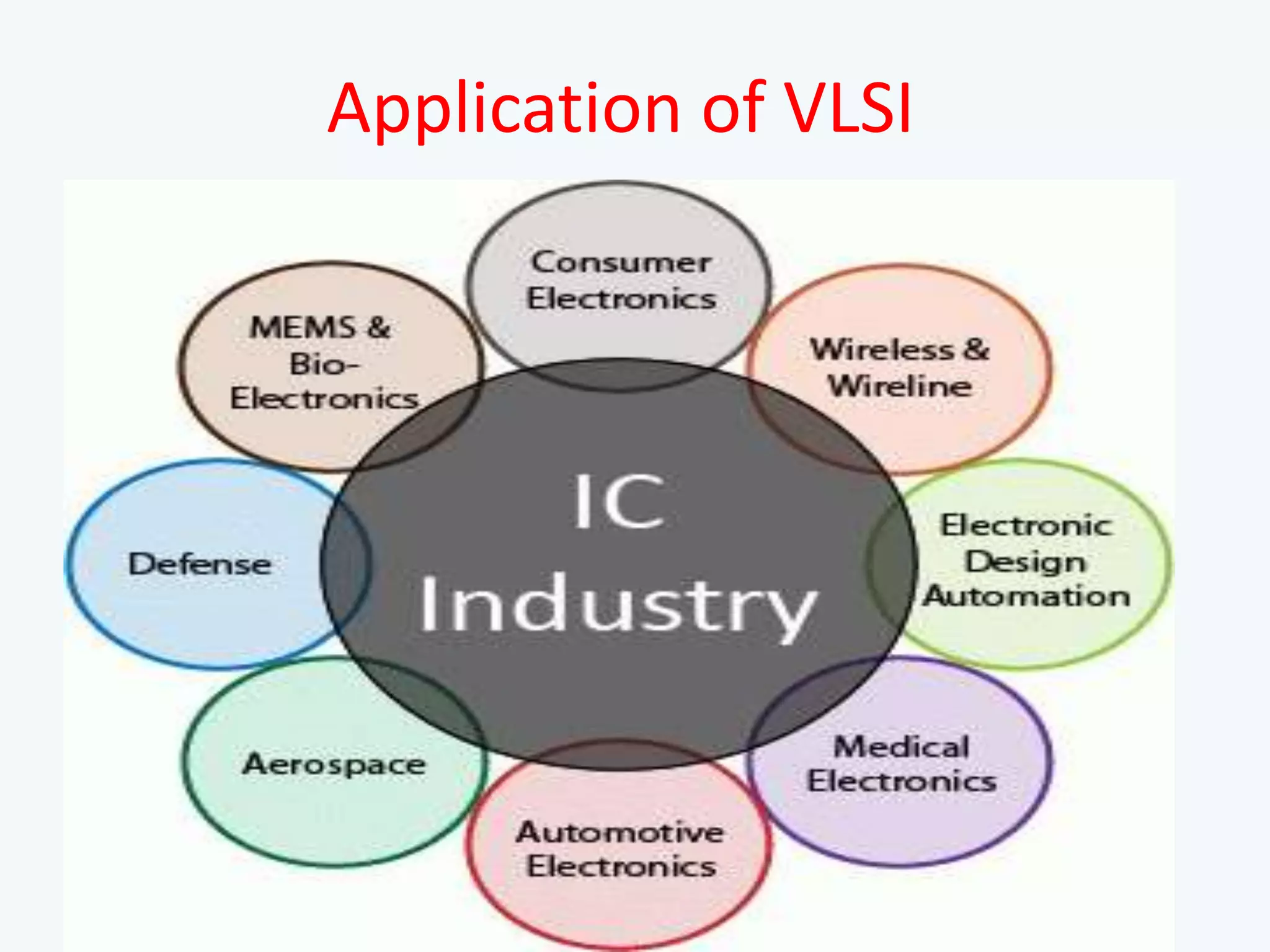
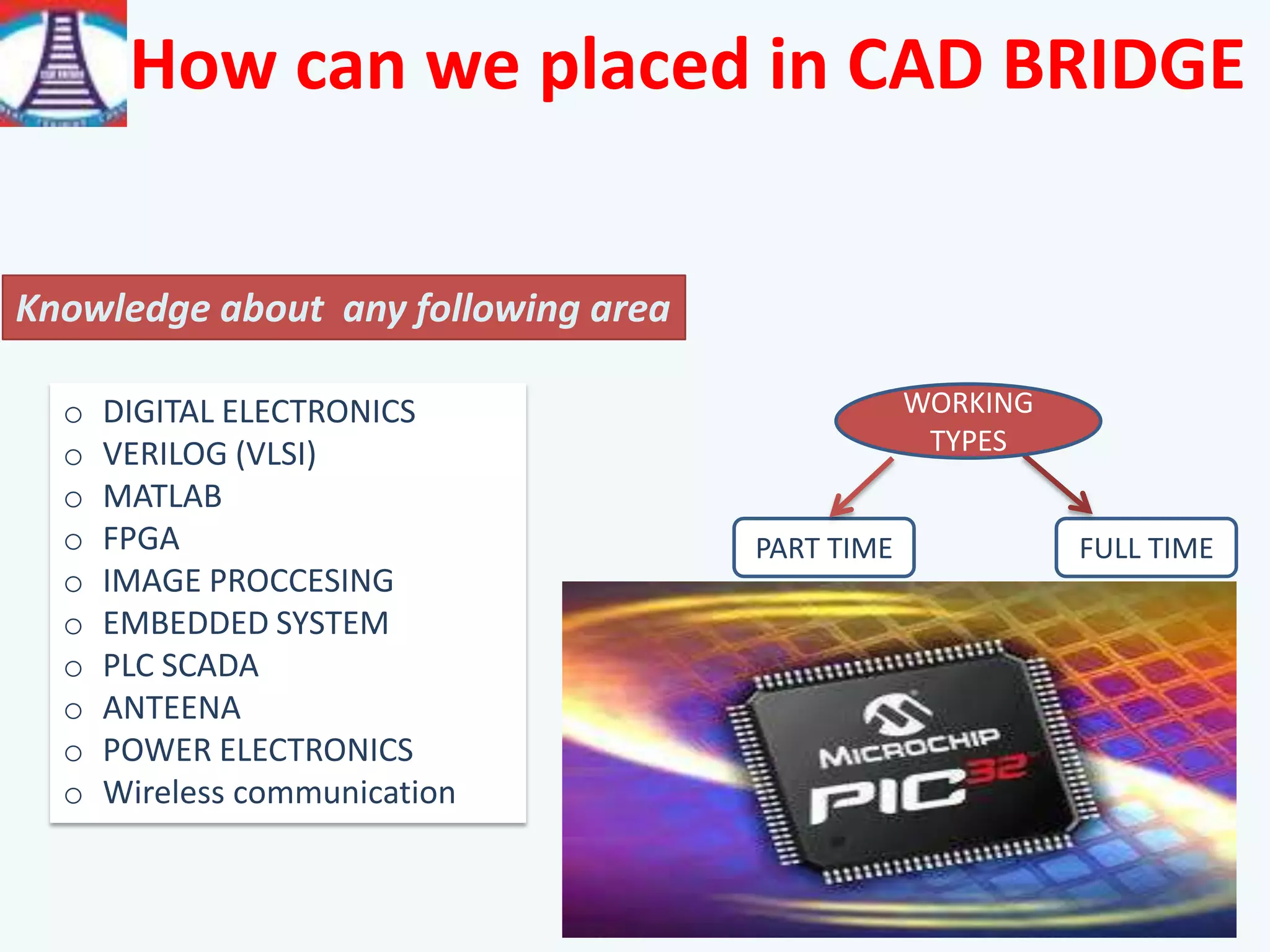


Cadbridge Semiconductor is an emerging electronics company with offices in Greater Noida and Jalander that works on projects involving memories, PCB design, digital security locks, robots, image processing, and microcontrollers. The company's vision is to hire and develop the best talent worldwide in a multicultural environment. The VLSI design flow presented includes idea conception, specification, design architecture, RTL coding, RTL verification, synthesis, sending to a foundry, and producing an IC chip. Application areas of VLSI discussed were microprocessors, memories, and mobile devices.


![Coded Agents – with UiPath SDK + LangGraph [Virtual Hands-on Workshop]](https://cdn.slidesharecdn.com/ss_thumbnails/codedagentsdeck-251215155422-5497c599-thumbnail.jpg?width=640&height=640&fit=bounds)


