SPICE MODEL of TPCP8402 (Professional+BDP N&P Model) in SPICE PARK
•
0 likes•172 views

SPICE MODEL of TPCP8402 (Professional+BDP N&P Model) in SPICE PARK. English Version is http://www.spicepark.net. Japanese Version is http://www.spicepark.com by Bee Technologies.

Recommended
Recommended
More Related Content
What's hot
What's hot (20)
Viewers also liked
Viewers also liked (20)
Similar to SPICE MODEL of TPCP8402 (Professional+BDP N&P Model) in SPICE PARK
Similar to SPICE MODEL of TPCP8402 (Professional+BDP N&P Model) in SPICE PARK (20)
More from Tsuyoshi Horigome
More from Tsuyoshi Horigome (20)
Recently uploaded
Recently uploaded (20)
SPICE MODEL of TPCP8402 (Professional+BDP N&P Model) in SPICE PARK
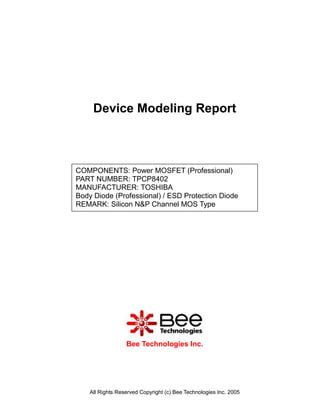
- 1. Device Modeling Report COMPONENTS: Power MOSFET (Professional) PART NUMBER: TPCP8402 MANUFACTURER: TOSHIBA Body Diode (Professional) / ESD Protection Diode REMARK: Silicon N&P Channel MOS Type Bee Technologies Inc. All Rights Reserved Copyright (c) Bee Technologies Inc. 2005
- 2. MOSFET MODEL Pspice model Model description parameter LEVEL L Channel Length W Channel Width KP Transconductance RS Source Ohmic Resistance RD Ohmic Drain Resistance VTO Zero-bias Threshold Voltage RDS Drain-Source Shunt Resistance TOX Gate Oxide Thickness CGSO Zero-bias Gate-Source Capacitance CGDO Zero-bias Gate-Drain Capacitance CBD Zero-bias Bulk-Drain Junction Capacitance MJ Bulk Junction Grading Coefficient PB Bulk Junction Potential FC Bulk Junction Forward-bias Capacitance Coefficient RG Gate Ohmic Resistance IS Bulk Junction Saturation Current N Bulk Junction Emission Coefficient RB Bulk Series Resistance PHI Surface Inversion Potential GAMMA Body-effect Parameter DELTA Width effect on Threshold Voltage ETA Static Feedback on Threshold Voltage THETA Modility Modulation KAPPA Saturation Field Factor VMAX Maximum Drift Velocity of Carriers XJ Metallurgical Junction Depth UO Surface Mobility All Rights Reserved Copyright (c) Bee Technologies Inc. 2005
- 3. P-Channel Model Transconductance Characteristic Circuit Simulation Result Comparison table gfs Id(A) Error(%) Measurement Simulation -0.500 4.000 4.025 0.625 -1.000 5.700 5.800 1.754 -2.000 7.000 7.036 0.514 -5.000 8.900 8.846 -0.606 All Rights Reserved Copyright (c) Bee Technologies Inc. 2005
- 4. Vgs-Id Characteristic Circuit Simulation result -8.0A -6.0A -4.0A -2.0A 0A 0V -1.0V -2.0V -3.0V -4.0V -5.0V -6.0V I(V3) V_V2 Evaluation circuit TPCP8402 V3 0Vdc open open open V1 open U16 open R1 V2 -10Vdc 0Vdc 100MEG 0 0 All Rights Reserved Copyright (c) Bee Technologies Inc. 2005
- 5. Comparison Graph Circuit Simulation Result Simulation Result VGS(V) ID(A) Error (%) Measurement Simulation -1.000 -2.150 -2.100 -2.325 -2.000 -2.320 -2.286 -1.465 -4.000 -2.600 -2.557 -1.653 -6.000 -2.800 -2.779 -0.750 -8.000 -3.000 -2.977 -0.767 All Rights Reserved Copyright (c) Bee Technologies Inc. 2005
- 6. Rds(on) Characteristic Circuit Simulation result -3.0A -2.5A -2.0A -1.5A -1.0A -0.5A 0A 0V -50mV -150mV -250mV -350mV -450mV I(V3) V_VDS Evaluation circuit TPCP8402 V3 0Vdc open open open open U16 open VGS 0Vdc VDS -4.5Vdc R1 100MEG 0 0 Simulation Result ID=-1.7A, VGS=-4.5V Measurement Simulation Error (%) R DS (on) 80.000 m 80.000 m 0.000 All Rights Reserved Copyright (c) Bee Technologies Inc. 2005
- 7. Gate Charge Characteristic Circuit Simulation result -15.00V -13.75V -12.50V -11.25V -12V -10.00V -8.75V -6V -7.50V VDD=-24V -6.25V -5.00V -3.75V -2.50V -1.25V 0V 0 2n 4n 6n 8n 10n 12n 14n 16n V(W1:2) Time*1ms Evaluation circuit TPCP8402 V2 ION = 0uA IOFF = 100uA 0Vdc W - open open open I1 = 0 + I1 open U16 open I2 = 1m W1 D1 TD = 0 TR = 10n I2 R1 TF = 10n Dbreak -3.4Adc PW = 600u 100MEG PER = 1000u V1 0 -24Vdc 0 Simulation Result VDD=-24V,ID=-3.4A Measurement Simulation Error (%) ,VGS=-10V Qgs 1.400 nC 1.393 nC -0.500 Qgd 2.700 nC 2.712 nC 0.445 Qg 14.000 nC 14.000 nC 0.000 All Rights Reserved Copyright (c) Bee Technologies Inc. 2005
- 8. Capacitance Characteristic Measurement Simulation Simulation Result Cbd(pF) VDS(V) Error(%) Measurement Simulation 0.200 45.000 44.300 -1.556 0.500 33.000 33.520 1.575 1.000 24.000 24.850 3.541 2.000 17.000 17.000 0.000 5.000 10.000 9.980 -0.200 10.000 7.000 6.870 -1.857 All Rights Reserved Copyright (c) Bee Technologies Inc. 2005
- 9. Switching Time Characteristic Circuit Simulation result -12V VDD =-15V Vg = 0/-10.0V -8V -4V 0V 4.96us 4.98us 5.00us 5.02us 5.04us 5.06us 5.08us V(2) V(3)/1.5 Time Evaluation circuit TPCP8402 RG L1 L2 R2 30nH 50nH 8.82 open 4.7 open open V1 = 0 V2 = -20 V2 R1 U16 R9 open open TD = 2u V1 4.7 -15Vdc 100MEG TR = 6n TF = 7n PW = 20u PER = 2000u 0 0 Simulation Result ID=-3.4A, VDD=-15V Measurement Simulation Error(%) VGS=0/10V ton 12.000 ns 11.935 ns -0.541 All Rights Reserved Copyright (c) Bee Technologies Inc. 2005
- 10. Output Characteristic Circuit Simulation result -10A -4.5V -3.5V -8A -6A -2.8V -2.7V -4A -2.6V -2A -2.5V VGS=-2.3V 0A 0V -1.0V -2.0V -3.0V -4.0V -5.0V I(Vdsense) V_Vvariable Evaluation circuit TPCP8402 Vdsense 0Vdc open Vstep open open Vv ariable open U16 open -10Vdc -10Vdc R1 100MEG 0 0 All Rights Reserved Copyright (c) Bee Technologies Inc. 2005
- 11. Forward Current Characteristic Circuit Simulation Result 10A 1.0A 100mA 0V 0.2V 0.4V 0.6V 0.8V 1.0V 1.2V I(V2) V_V3 Evaluation Circuit R1 0.01m openopen open U16 V1 0Vdc TPCP8402 Ropen 100MEG openopen 0 0 All Rights Reserved Copyright (c) Bee Technologies Inc. 2005
- 12. Comparison Graph Circuit Simulation Result Simulation Result Vfwd(V) Vfwd(V) Ifwd(A) Measurement Simulation %Error 0.100 0.600 0.605 0.833 0.200 0.660 0.653 -1.061 0.500 0.720 0.718 -0.278 1.000 0.780 0.769 -1.410 2.000 0.830 0.820 -1.205 5.000 0.940 0.904 -3.830 All Rights Reserved Copyright (c) Bee Technologies Inc. 2005
- 13. Reverse Recovery Characteristic Circuit Simulation Result 400mA 300mA 200mA 100mA -0mA -100mA -200mA -300mA -400mA 0.958us 1.000us 1.050us 1.098us I(R1) Time Evaluation Circuit R1 50 V1 = {-9.7} V2 = {10.6} TD = 5.0799n V1 TR = 10n D8402_P TF = 10n PW = 15u PER = 100u 0 0 Compare Measurement vs. Simulation Measurement Simulation Error (%) trj 5.200 ns 5.160 ns -0.769 trb 10.400 ns 10.400 ns 0.000 trr 15.600 ns 5.240 ns -2.307 All Rights Reserved Copyright (c) Bee Technologies Inc. 2005
- 14. Reverse Recovery Characteristic Reference Trj=5.2(ns) Trb=10.4(ns) Conditions:Ifwd=lrev=0.2(A),Rl=50 Example Relation between trj and trb All Rights Reserved Copyright (c) Bee Technologies Inc. 2005
- 15. Zener Voltage Characteristic Circuit Simulation Result -10mA -9mA -8mA -7mA -6mA -5mA -4mA -3mA -2mA -1mA 0A 0V -5V -10V -15V -20V -25V -30V -35V -40V -45V I(R1) V_V1 Evaluation Circuit R1 0.01m TPCP8402 open open V1 open 0Vdc Ropen open open 100MEG open U16 open 0 0 All Rights Reserved Copyright (c) Bee Technologies Inc. 2005
- 16. Zener Voltage Characteristic Reference All Rights Reserved Copyright (c) Bee Technologies Inc. 2005
- 17. N-Channel Model Transconductance Characteristic Circuit Simulation Result Comparison table gfs Id(A) Error(%) Measurement Simulation 0.500 3.000 3.100 3.333 1.000 5.000 5.181 3.620 2.000 7.000 6.898 -1.457 5.000 9.300 9.572 2.924 All Rights Reserved Copyright (c) Bee Technologies Inc. 2005
- 18. Vgs-Id Characteristic Circuit Simulation result 8.0A 6.0A 4.0A 2.0A 0A 0V 1.0V 2.0V 3.0V 4.0V 5.0V 6.0V I(V3) V_V2 Evaluation circuit U16 V3 0Vdc open open open open open V1 TPCP8402 10Vdc R1 V2 0Vdc 100MEG 0 0 All Rights Reserved Copyright (c) Bee Technologies Inc. 2005
- 19. Comparison Graph Circuit Simulation Result Simulation Result VGS(V) ID(A) Error (%) Measurement Simulation 1.000 2.700 2.697 -0.111 2.000 2.900 2.896 -0.138 4.000 3.200 3.206 0.187 6.000 3.500 3.462 -1.086 8.000 3.700 3.691 -0.243 All Rights Reserved Copyright (c) Bee Technologies Inc. 2005
- 20. Rds(on) Characteristic Circuit Simulation result 2.0A 1.0A 0A 0V 50mV 100mV 150mV 200mV 250mV 300mV 350mV 400mV 450mV I(V3) V_V2 Evaluation circuit U16 V3 0Vdc open open open open open VGS 0Vdc VDS Ropen 4.5Vdc TPCP8402 100MEG 0 0 Simulation Result ID=3.1A, VGS=4.5V Measurement Simulation Error (%) R DS (on) 58.000 m 5.969 m -0.053 All Rights Reserved Copyright (c) Bee Technologies Inc. 2005
- 21. Gate Charge Characteristic Circuit Simulation result 15.00V 13.75V 12.50V 11.25V 10.00V 8.75V 7.50V 6.25V 5.00V 3.75V 2.50V 1.25V 0V 0 2n 4n 6n 8n 10n 12n 14n 16n V(W1:2) Time*1ms Evaluation circuit U16 V2 0Vdc open open open Dbreak PER = 1000u W1 open open PW = 600u + TF = 10n D1 - TR = 10n TPCP8402 I2 Ropen TD = 0 W 6Adc I2 = 1m IOFF = 100uA 100MEG I1 ION = 0uA I1 = 0 V1 0 24Vdc 0 Simulation Result VDD=24V,ID=6A Measurement Simulation Error (%) ,VGS=10V Qgs 1.700 nC 1.658 nC -2.470 Qgd 2.400 nC 2.400 nC 0.000 Qg 10.000 nC 10.000 nC 0.000 All Rights Reserved Copyright (c) Bee Technologies Inc. 2005
- 22. Capacitance Characteristic Measurement Simulation Simulation Result Cbd(pF) VDS(V) Error(%) Measurement Simulation 0.100 120.000 120.000 0.000 0.200 105.000 106.215 1.157 0.500 80.000 81.540 1.925 1.000 60.000 60.876 1.460 2.000 42.000 43.052 2.505 5.000 25.000 25.000 0.000 10.000 16.000 16.120 0.750 All Rights Reserved Copyright (c) Bee Technologies Inc. 2005
- 23. Switching Time Characteristic Circuit Simulation result 12V VDD = 15V Vg = 0/10.0V 8V 4V 0V 4.96us 4.98us 5.00us 5.02us 5.04us 5.06us 5.08us V(2) V(3)/1.5 Time Evaluation circuit U16 L2 R2 RG L1 50nH 7.14 30nH open open open 4.7 open open V1 = 0 V2 = 20 V2 R1 TD = 2u TPCP8402 V1 Ropen 4.7 15Vdc TR = 6n 100MEG TF = 7n PW = 20u PER = 2000u 0 0 Simulation Result ID=2.1 A, VDD=15V Measurement Simulation Error(%) VGS=0/10V ton 8.300 ns 8.700 ns 4.819 All Rights Reserved Copyright (c) Bee Technologies Inc. 2005
- 24. Output Characteristic Circuit Simulation result 10A 10V, 8V 4.5V 9A 6V 8A 3.8V 7A 6A 3.5V 5A 4A 3A 3.2V 2A 3.0V 1A VGS=2.8V 0A 0V 0.5V 1.0V 1.5V 2.0V 2.5V 3.0V 3.5V 4.0V 4.5V I(V3) V_V2 Evaluation circuit Vdsense U16 0Vdc Vv ariable Vstep open open 10Vdc open open open 10Vdc TPCP8402 R1 100MEG 0 0 All Rights Reserved Copyright (c) Bee Technologies Inc. 2005
- 25. Forward Current Characteristic Circuit Simulation Result 10A 1.0A 100mA 0V 0.2V 0.4V 0.6V 0.8V 1.0V 1.2V I(R1) V_V1 Evaluation Circuit R1 0.01m openopen open V1 0Vdc TPCP8402 Ropen U16 100MEG openopen 0 0 All Rights Reserved Copyright (c) Bee Technologies Inc. 2005
- 26. Comparison Graph Circuit Simulation Result Simulation Result Vfwd(V) Vfwd(V) Ifwd(A) Measurement Simulation %Error 0.100 0.710 0.706 - 0.563 0.200 0.720 0.723 0.416 0.500 0.750 0.750 0.000 1.000 0.780 0.780 0.000 2.000 0.820 0.820 0.000 5.000 0.910 0.908 - 0.219 10.000 1.020 1.020 0.000 All Rights Reserved Copyright (c) Bee Technologies Inc. 2005
- 27. Reverse Recovery Characteristic Circuit Simulation Result 400mA 300mA 200mA 100mA -0mA -100mA -200mA -300mA -400mA 0.958us 1.000us 1.050us 1.098us I(R1) Time Evaluation Circuit R1 50 V1 = {-9.7} V2 = {10.6} TD = 5.0799n V1 TR = 10n D8402_N TF = 10n PW = 15u PER = 100u 0 0 Compare Measurement vs. Simulation Measurement Simulation Error (%) trj 4.800 ns 4.800 ns 0.000 trb 11.600 ns 11.600 ns 0.000 trr 16.400 ns 16.400 ns 0.000 All Rights Reserved Copyright (c) Bee Technologies Inc. 2005
- 28. Reverse Recovery Characteristic Reference Trj=4.8(ns) Trb=11.6(ns) Conditions:Ifwd=lrev=0.2(A),Rl=50 Example Relation between trj and trb All Rights Reserved Copyright (c) Bee Technologies Inc. 2005
- 29. Zener Voltage Characteristic Circuit Simulation Result 10mA 9mA 8mA 7mA 6mA 5mA 4mA 3mA 2mA 1mA 0A 0V 5V 10V 15V 20V 25V 30V 35V 40V 45V 50V I(R1) V_V1 Evaluation Circuit R1 0.01m U16 open open open V1 open open Ropen 0Vdc open 100MEG open TPCP8402 0 0 All Rights Reserved Copyright (c) Bee Technologies Inc. 2005
- 30. Zener Voltage Characteristic Reference All Rights Reserved Copyright (c) Bee Technologies Inc. 2005