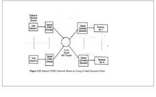
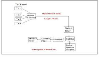
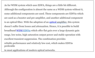
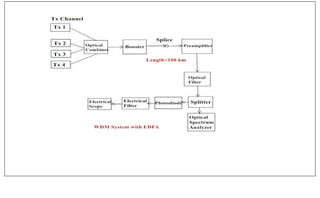
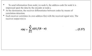
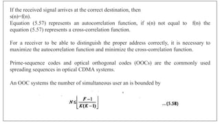
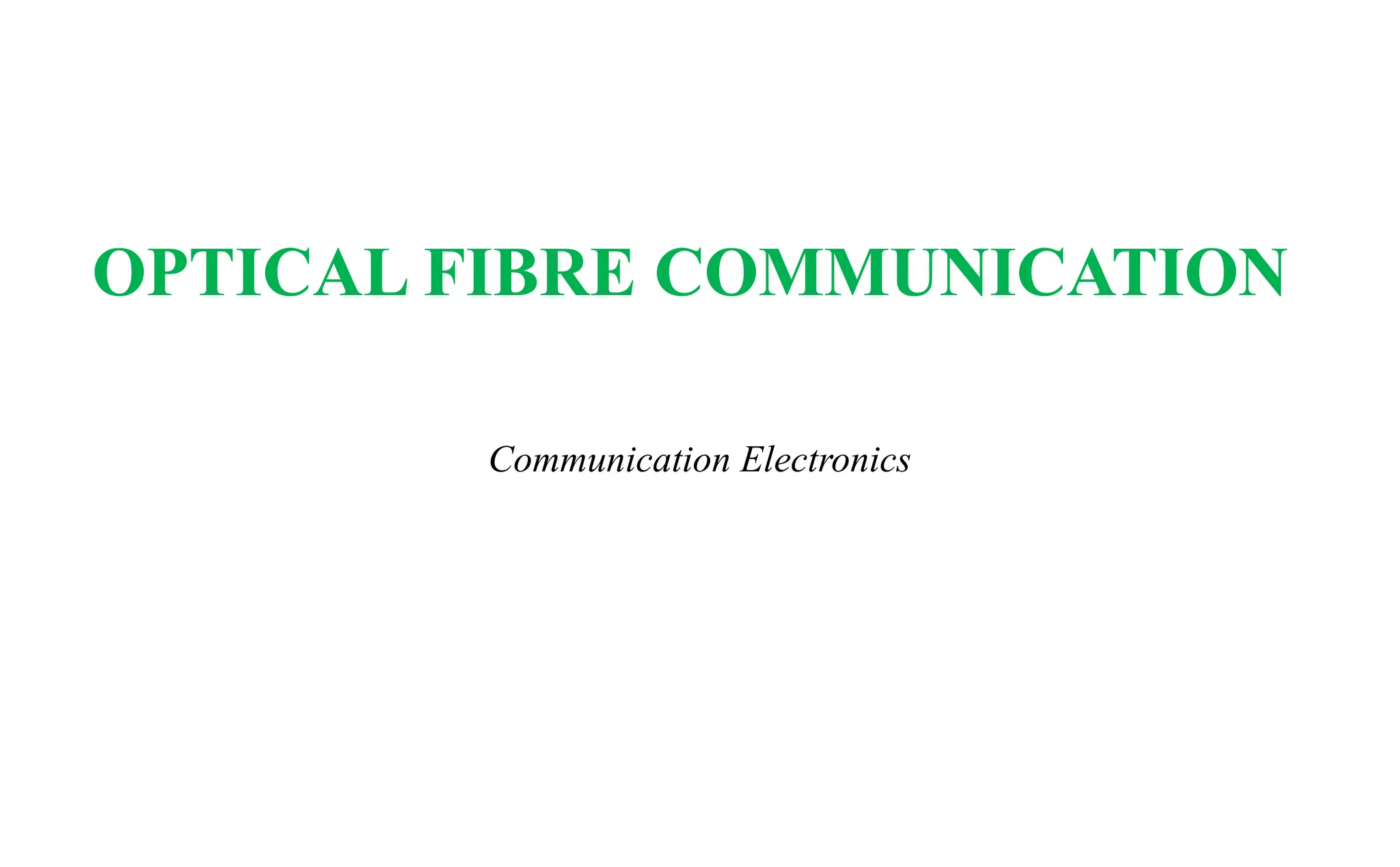
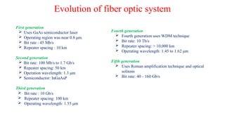
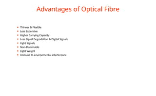
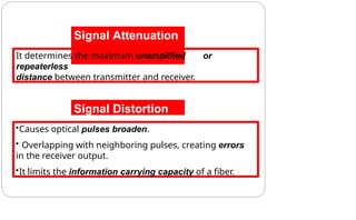
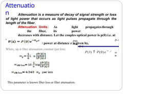
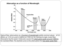
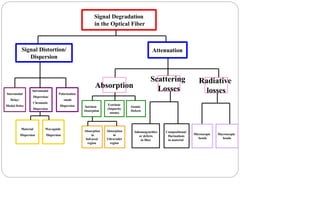
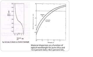
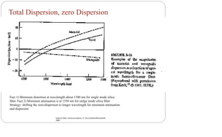
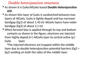
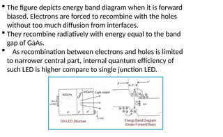
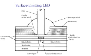
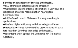
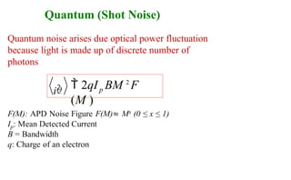
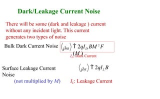
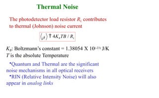
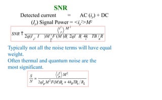
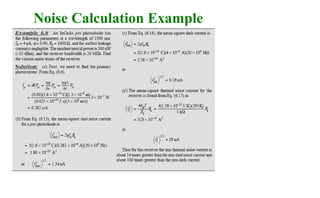
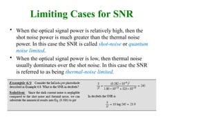
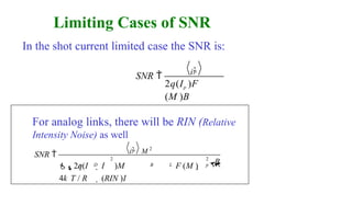
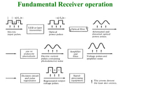
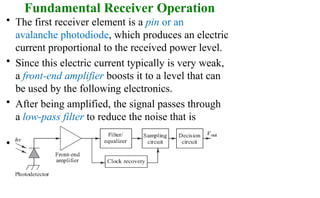
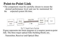
The document provides a comprehensive overview of optical fiber communication, highlighting its evolution through five generations with varying bit rates, operating wavelengths, and technologies. It discusses the advantages and disadvantages of optical fibers, their applications in various fields, and the principles governing their operation, including refraction and internal reflection. Additionally, it covers factors affecting signal attenuation and distortion in optical fibers, emphasizing key characteristics and performance metrics.

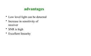
![is called GVD parameter, and shows how much a light pulse
broadens as it travels along an optical fiber.
The more common parameter is called Dispersion, and can be
defined as
the delay difference per unit length per unit wavelength as follows
The pulse spreading σg of fiber length of L, can be well
approximated by:
D has a typical unit of
[ps/(nm.km)].
2
2
2
c
g
1 d g d 1
L d d V
D
d
g
DL
d g
](https://image.slidesharecdn.com/r20ofcref-241110101118-23e12289/85/Optical-Fiber-Communication-R20-_OFC-ref-pptx-46-320.jpg)
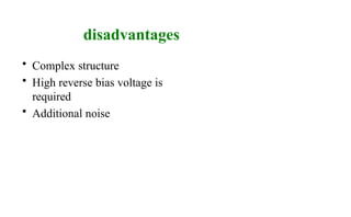
![Fabry-Perot
Resonator
A
B
L
M1 M2 m = 1
m = 2
m = 8
Relative intensity
υ
υm + 1
υm - 1
(a)
υm
(c)
R ~ 0.4
δυm
R ~
0.8
1 υf
(1−R)2
+4R sin2
(kL)
Schematic illustration of the Fabry-Perot optical cavity and its properties. (a) Reflected
waves interfere. (b) Only standing EM waves, modes, of certain wavelengths are allowed
in the cavity. (c) Intensity vs. frequency for various modes. R is mirror reflectance and
lower R means higher loss from the cavity.
© 1999 S.O. Kasap, Optoelectronics (Prentice Hall)
(1−R)2
Itrans
=Iinc
[4-18]
R: reflectance of the optical intensity, k: optical wavenumber
(b)
Resonant modes : kL =m m
=1,2,3,..](https://image.slidesharecdn.com/r20ofcref-241110101118-23e12289/85/Optical-Fiber-Communication-R20-_OFC-ref-pptx-92-320.jpg)

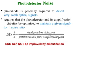
![Rate
equations
Rate equations relate the optical output power, or
# of photons per unit volume, Φ , to the diode
drive current or # of injected electrons per
unit volume, n. For active (carrier confinement)
region of depth d, the rate equations are:
–
Φ
dΦ =Cn Φ
+R
dt
ph
sp
τ
Photon rate =stimulated emission +spontaneou s emission +
photon loss
– n
−CnΦ
dn = J
dt
qd
τsp
[4-25]](https://image.slidesharecdn.com/r20ofcref-241110101118-23e12289/85/Optical-Fiber-Communication-R20-_OFC-ref-pptx-100-320.jpg)
![Threshold current Density & excess electron
density
≈
0
•
At the threshold of lasing: Φ ≈0, dΦ/ dt ≥0,
Rsp
ph
=
n
th
C
τ
1
from eq.[4 - 25] ⇒ CnΦ
Φ
− /τ
ph ≥0 ⇒
n ≥
[4-26]
• The threshold current needed to maintain a steady state
threshold concentration of the excess electron, is found from
electron rate equation under steady state condition dn/dt=0
when the laser is just about to lase:
sp
th
sp τ
0 = −
qd
τ
⇒ J =qd
nth
Jth nth [4-27]](https://image.slidesharecdn.com/r20ofcref-241110101118-23e12289/85/Optical-Fiber-Communication-R20-_OFC-ref-pptx-101-320.jpg)
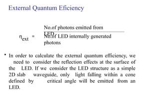
![External quantum efficiency
• Number of photons emitted per radiative electron-hole
pair recombination above threshold, gives us the external
quantum efficiency.
ext
η =ηi (gth
−α)
gth
[4-29]](https://image.slidesharecdn.com/r20ofcref-241110101118-23e12289/85/Optical-Fiber-Communication-R20-_OFC-ref-pptx-103-320.jpg)
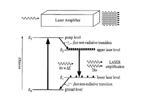
![Resonant
Frequencies
• Lasing condition:
exp(− j2βL) =1 ⇒ 2βL
=2mπ,
• Assuming
β =
2πn
mode is:
the resonant frequency of the
mth
m
=1,2,3,...
m
=1,2,3,...
= mc
2Ln
ν
m
c
⇔ ∆λ = λ2
2Ln 2Ln
− ν
=
m m−1
∆ν
=ν
[4-30]
[4-31]](https://image.slidesharecdn.com/r20ofcref-241110101118-23e12289/85/Optical-Fiber-Communication-R20-_OFC-ref-pptx-104-320.jpg)
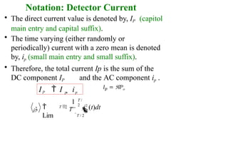
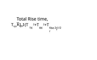
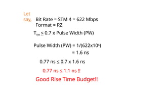
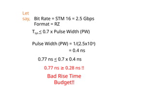
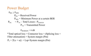
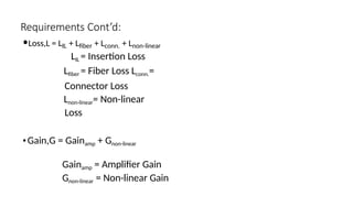
![Rise-Time Budget
1/ 2
2
B0
2
2
1/ 2
tGVD trx ]
Brx
L2
2
350
q
2
440L
2
ttx
2
2
tsys [ttx tmod
[nm]:Spectral width of the
source
D[ns /(km.nm)]:Dispersion
q0.7
ttx [ns] : transmitter rise time
Brx [ MHz]:3dB ElectricalBW
t rx
[ns] : receiver rise time t mod
[n] : modal dispersion
L[km ]:Length of the fiber B0 [ MHz]:BW of the1 km of the
fiber;
tGVD [ns]: rise-time due to groupvelocitydispersion](https://image.slidesharecdn.com/r20ofcref-241110101118-23e12289/85/Optical-Fiber-Communication-R20-_OFC-ref-pptx-160-320.jpg)