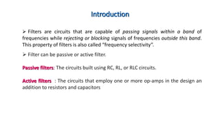
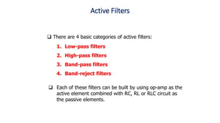
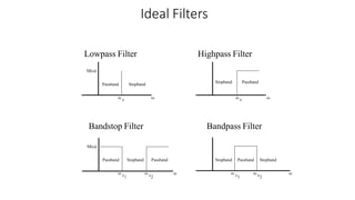
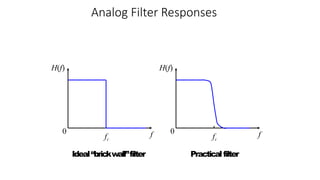
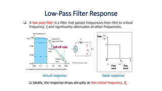
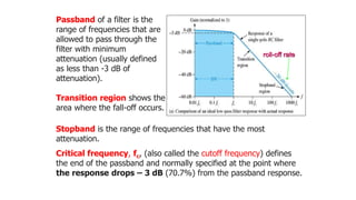
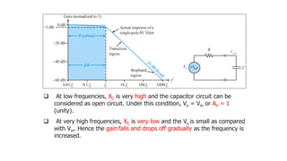
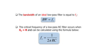
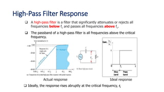
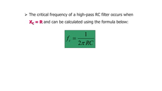
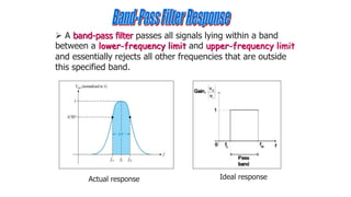
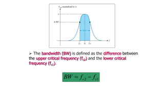
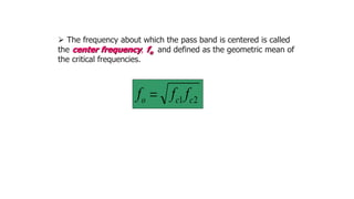
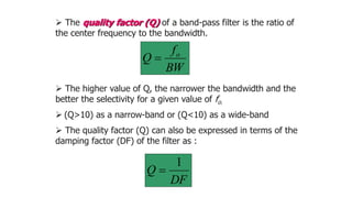
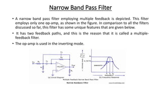
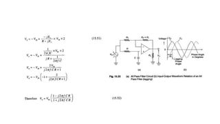
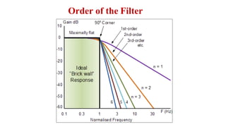
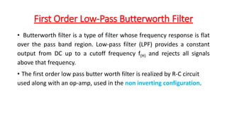
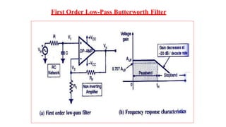
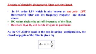
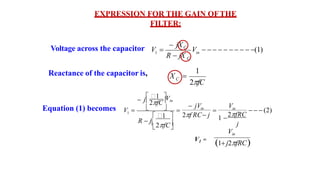
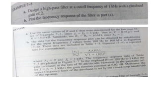
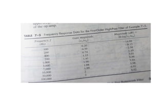
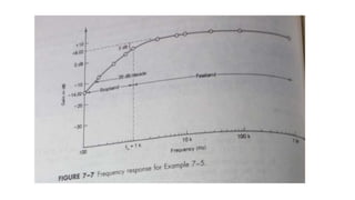
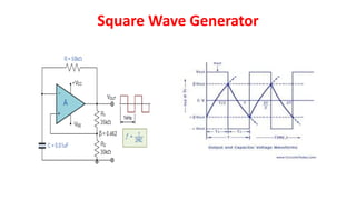
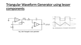
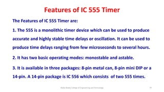
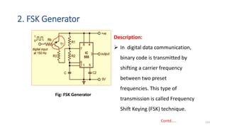
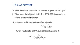
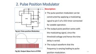
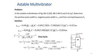
The document discusses the characteristics and applications of active and passive filters, including low-pass, high-pass, band-pass, and band-reject configurations using operational amplifiers (op-amps). It details the advantages of active filters over passive filters and provides design methodologies, including the calculation of cutoff frequencies and gain for Butterworth filters. Additionally, it covers waveform generators like square, triangular, and sawtooth, emphasizing their operational principles and components.
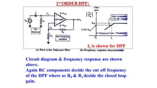
![Determine the gain of the first order low pass filter if the phase angle is 59.77o and the
pass band gain is 7.
Explanation: Given the phase angle, φ =-tan-1(f/fH)
=> f/fH=- φtan(φ) = -tan(59.77o)
=> f/fH= -1.716.
Substituting the above value in gain of the filter, |(VO/Vin)| = AF/√ (1+(f/fH)2) =7/√[1+(-1.716)2)]
=7/1.986
=>|(VO/Vin)|=3.5.](https://image.slidesharecdn.com/unit-iifiltersldic-240617030703-e1c97dea/85/LINEAR-INTEGRATED-CIRCUITS-UNIT-2-FILTERS-AND-DESIGN-44-320.jpg)
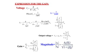

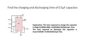
![Astable Multivibrator- Analysis
109
C
R
t B
LOW
69
.
0
After solving, we get, t=0.69RC
For the given circuit,
Both RA and RB are in the charge path, but only RB is in the discharge path.
The total time period,
C
C
T R
R
R
t
t B
B
LOW
HIGH A 69
.
0
)
69
.
0 (
C
C
C
C
T R
R
R
R
R
R
R
R A
A
A B
B
B
B
B
)
69
.
0
)
69
.
0
]
)
69
.
0 2
(
(
[(
C
C
T
f
R
R
R
R A
A B
B
)
45
.
1
)
69
.
0
1
1
2
(
2
(
Frequency,
Duty Cycle,
100
)
)
100
)
69
.
0
)
69
.
0
100
%
2
(
(
2
(
(
X
X
C
C
X
T
D
R
R
R
R
R
R
R
R
t
A
A
A
A
B
B
B
B
HIGH
100
)
100
)
69
.
0
69
.
0
100
%
2
(
2
(
X
X
C
C
X
T
D
R
R
R
R
R
R
t
A
A B
B
B
B
LOW
…… Discharging time
…….1.45 is Error Constant](https://image.slidesharecdn.com/unit-iifiltersldic-240617030703-e1c97dea/85/LINEAR-INTEGRATED-CIRCUITS-UNIT-2-FILTERS-AND-DESIGN-109-320.jpg)
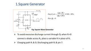
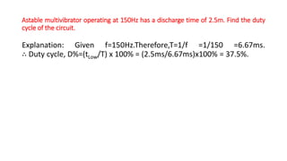
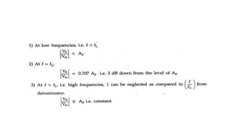
![Determine the frequency and duty cycle of a rectangular wave generator.
Explanation: Frequency=1.45/(RA+RB)C .
Where RA=100Ω+50Ω=150Ω,
RB=100Ω+20Ω=120Ω.
=>∴f=1.45/((150+120)x0.1µF) = 53703Hz = 53.7kHz.
Duty cycle, D% = [RB/(RA+RB)] x 100% = 120Ω/(150Ω +120Ω) x 100% =
0.55×100% = 55%.](https://image.slidesharecdn.com/unit-iifiltersldic-240617030703-e1c97dea/85/LINEAR-INTEGRATED-CIRCUITS-UNIT-2-FILTERS-AND-DESIGN-121-320.jpg)
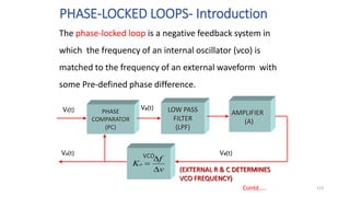
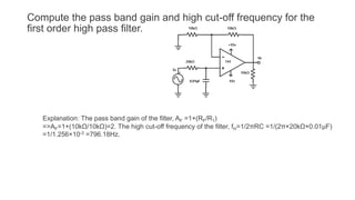
![PLL-Basic Components
131
Phase detector:
Transfer function: KΦ [V/radians].
Implemented as: four quad
multiplier, XOR gate, state
machine.
Voltage controlled oscillator (VCO):
Frequency is the first derivative of
phase.
Transfer function: KVCO/s
[radians/(V•s)]
Low pass filter:
Removes high frequency components coming from the phase detector.
Determines loop order and loop dynamics.](https://image.slidesharecdn.com/unit-iifiltersldic-240617030703-e1c97dea/85/LINEAR-INTEGRATED-CIRCUITS-UNIT-2-FILTERS-AND-DESIGN-131-320.jpg)