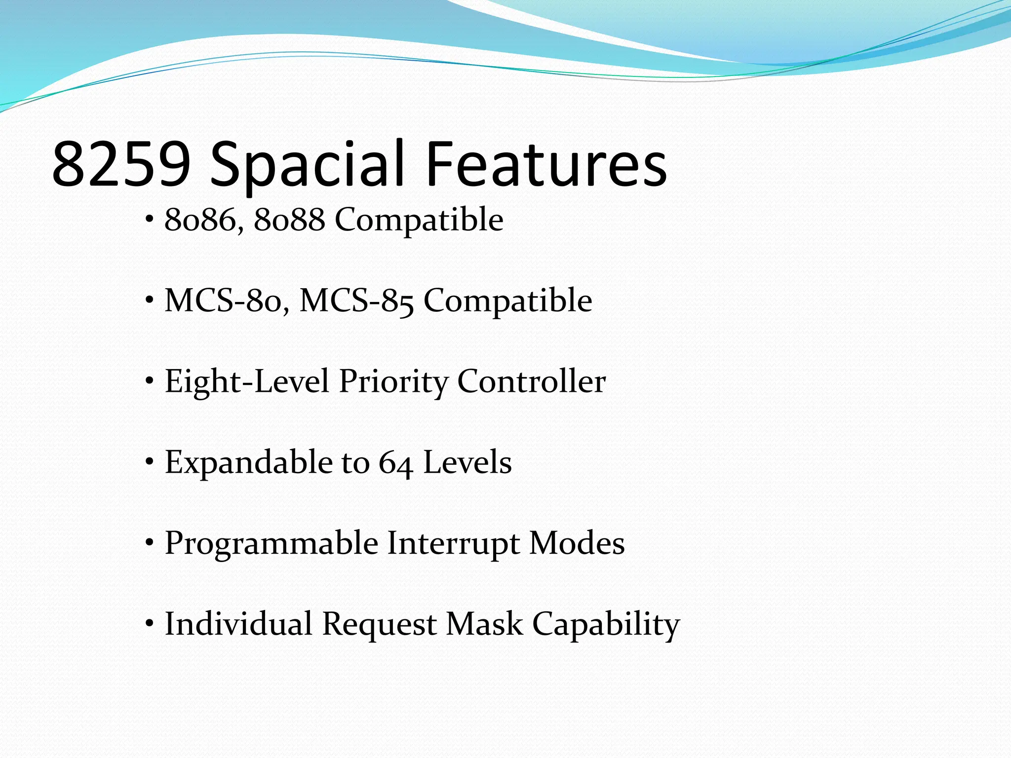
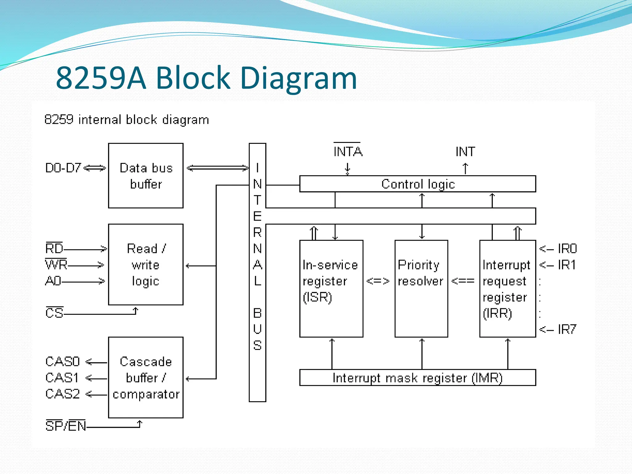
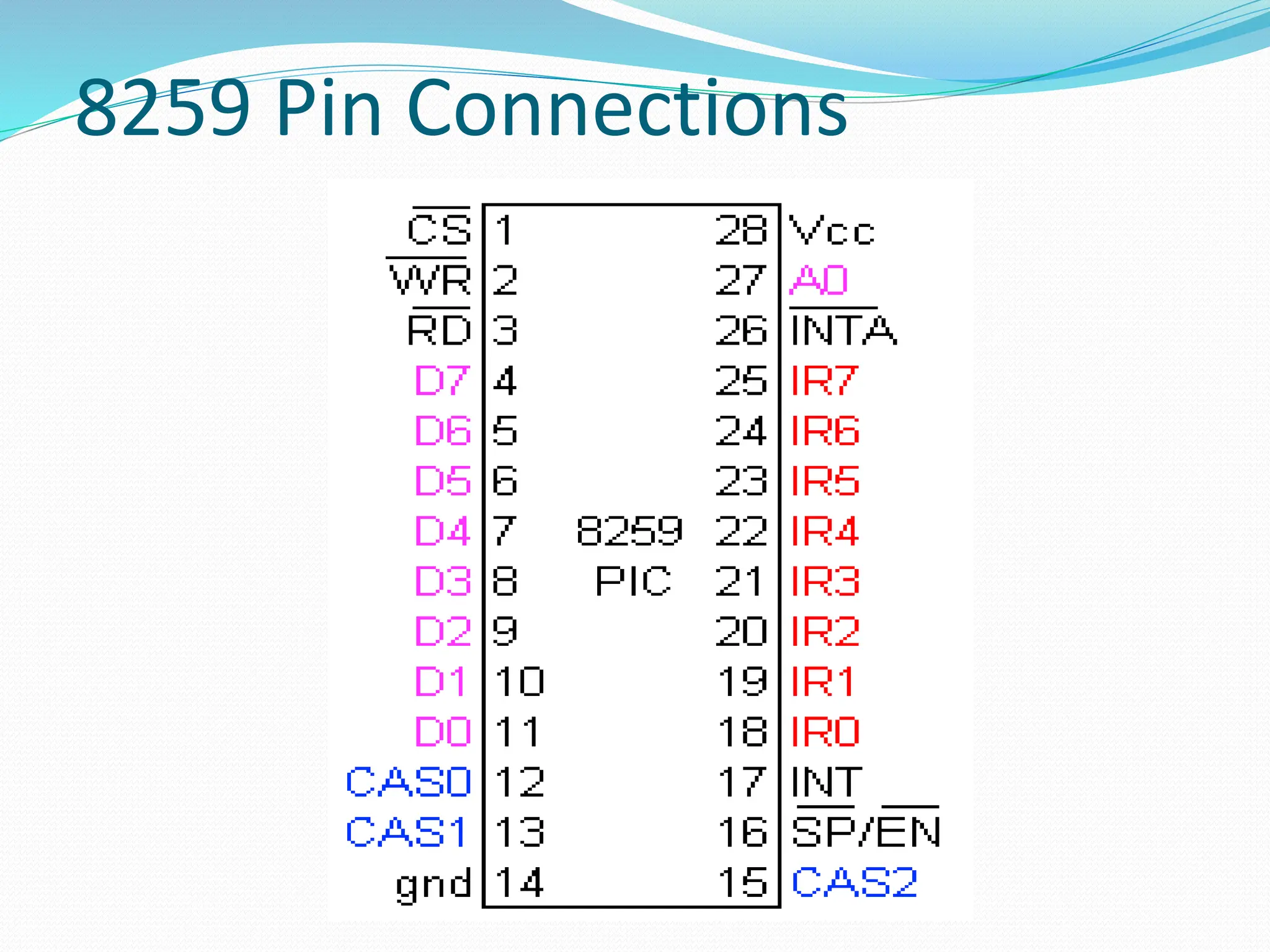
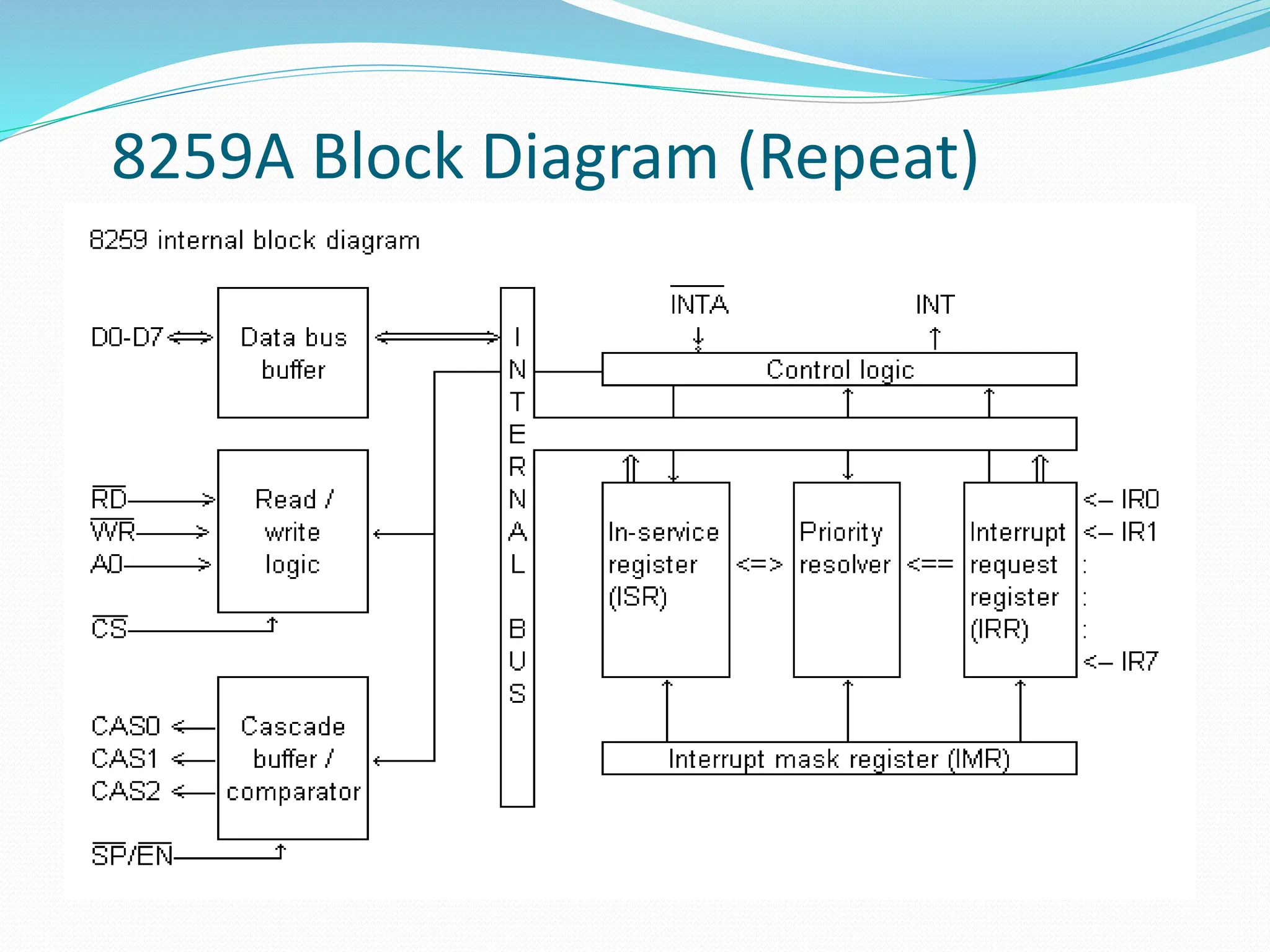
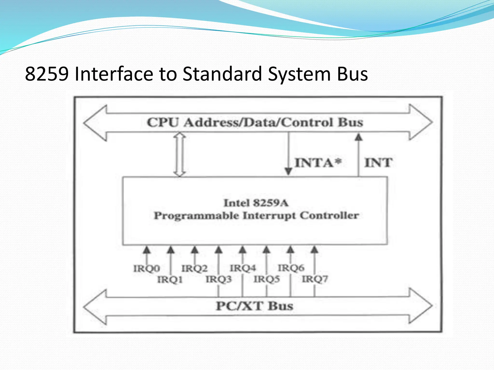
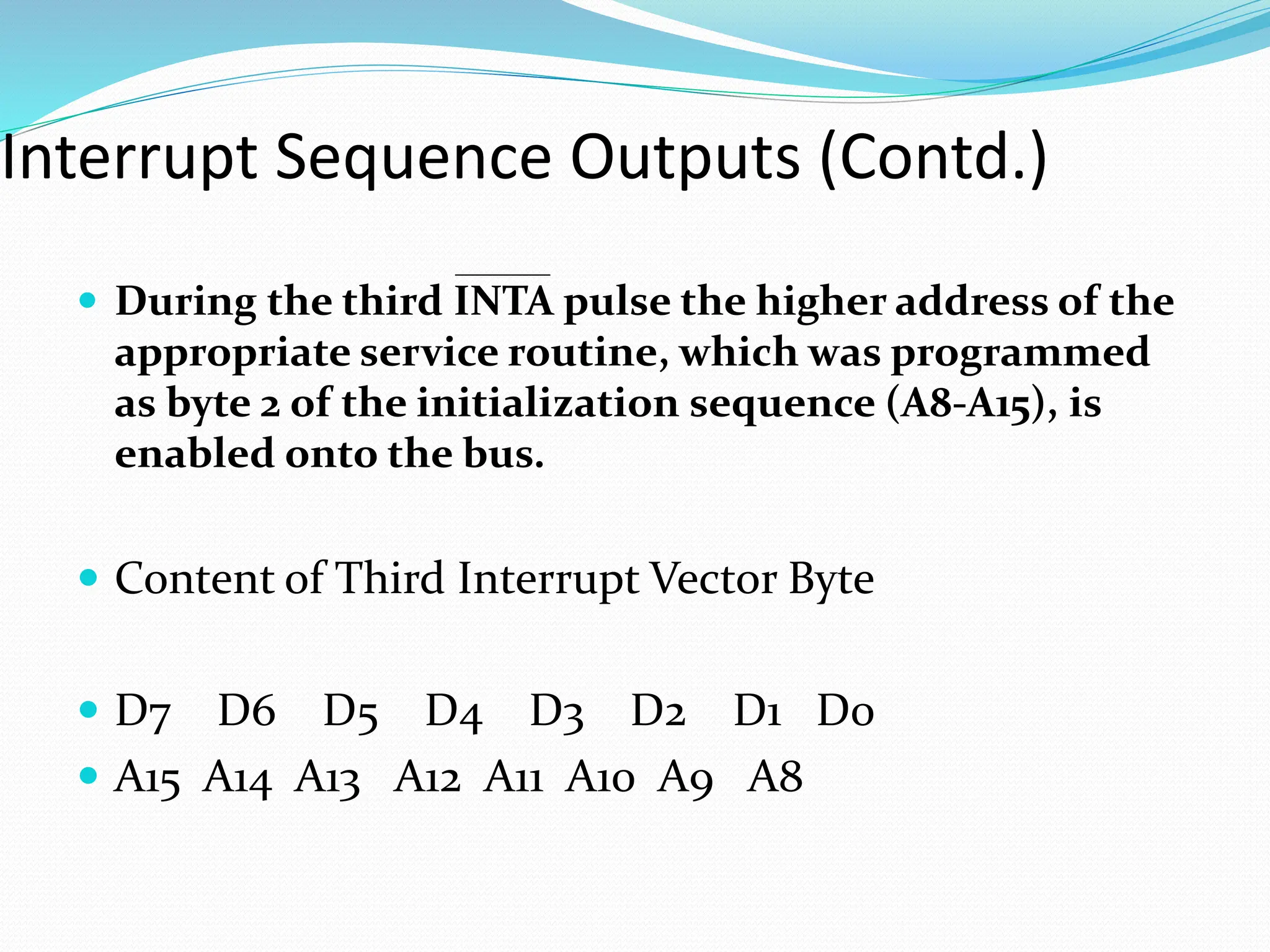
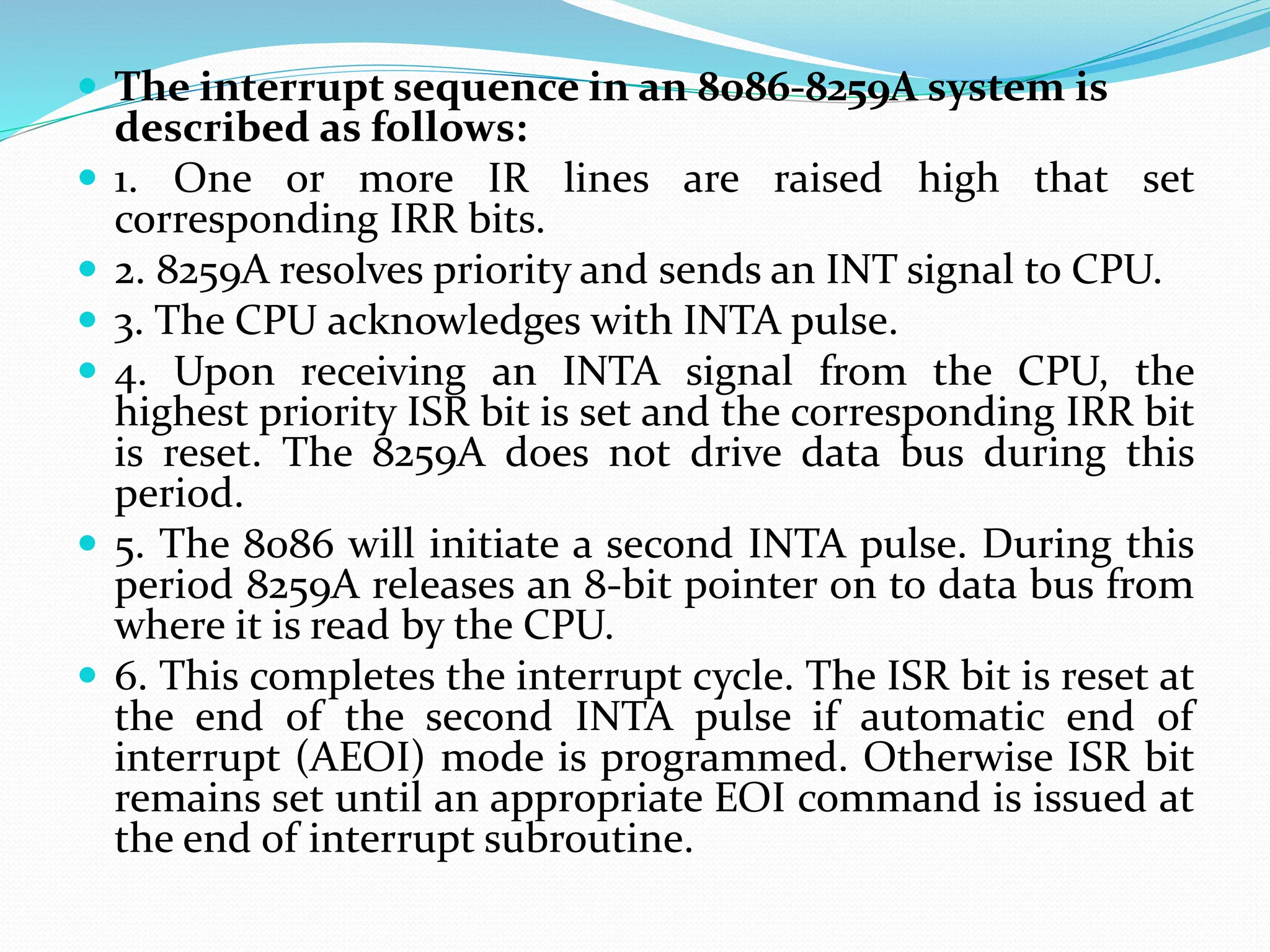
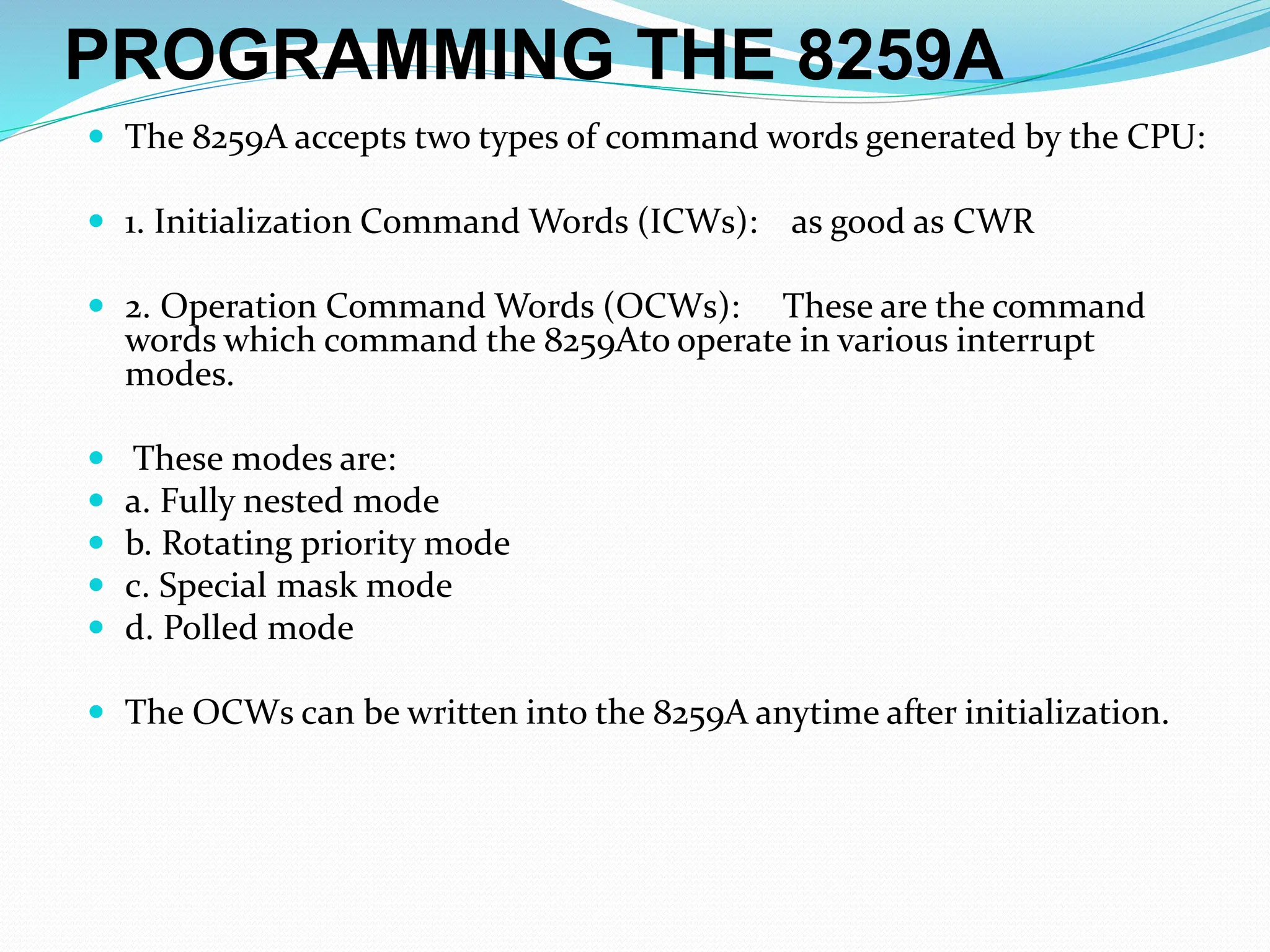
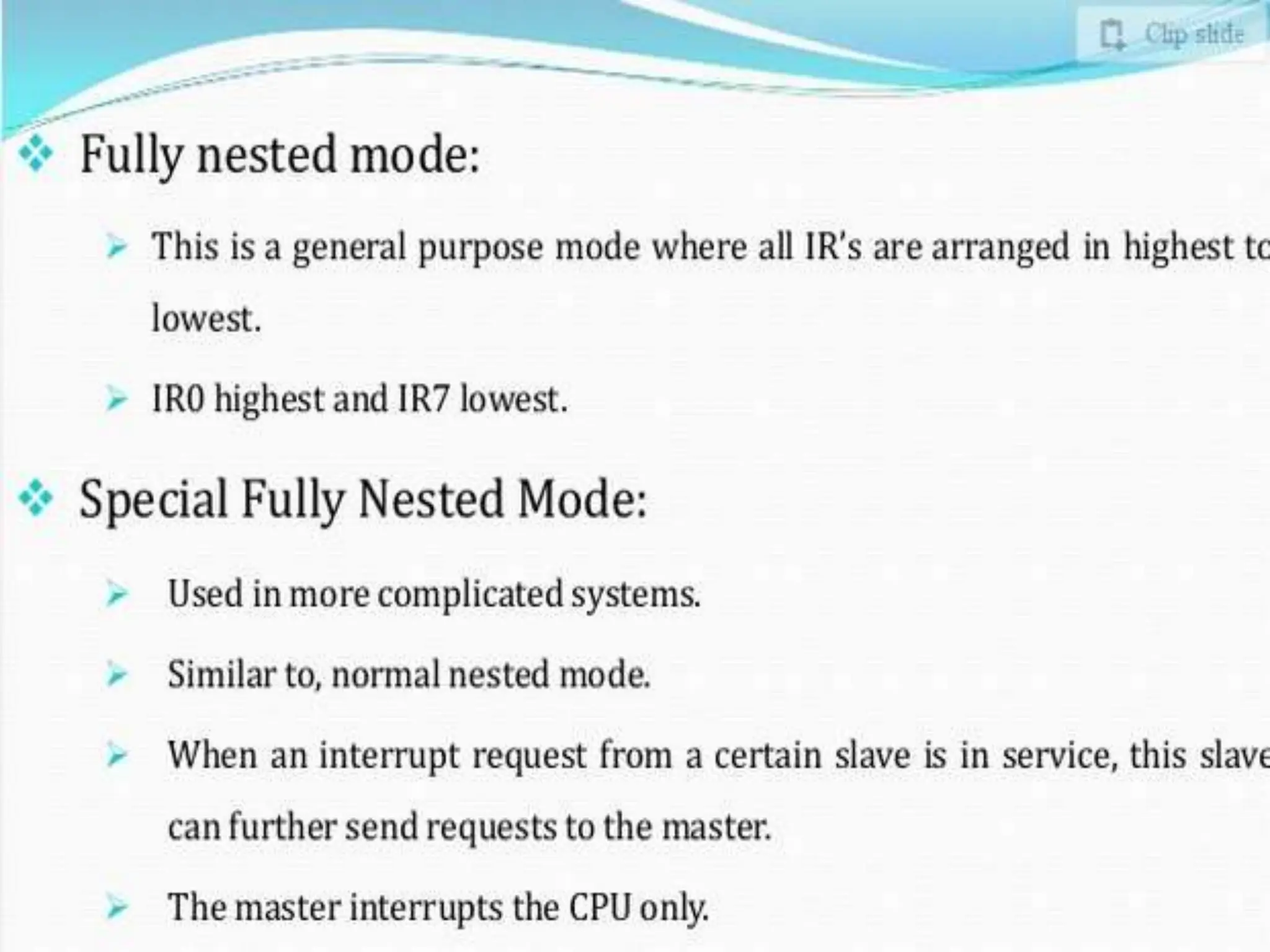
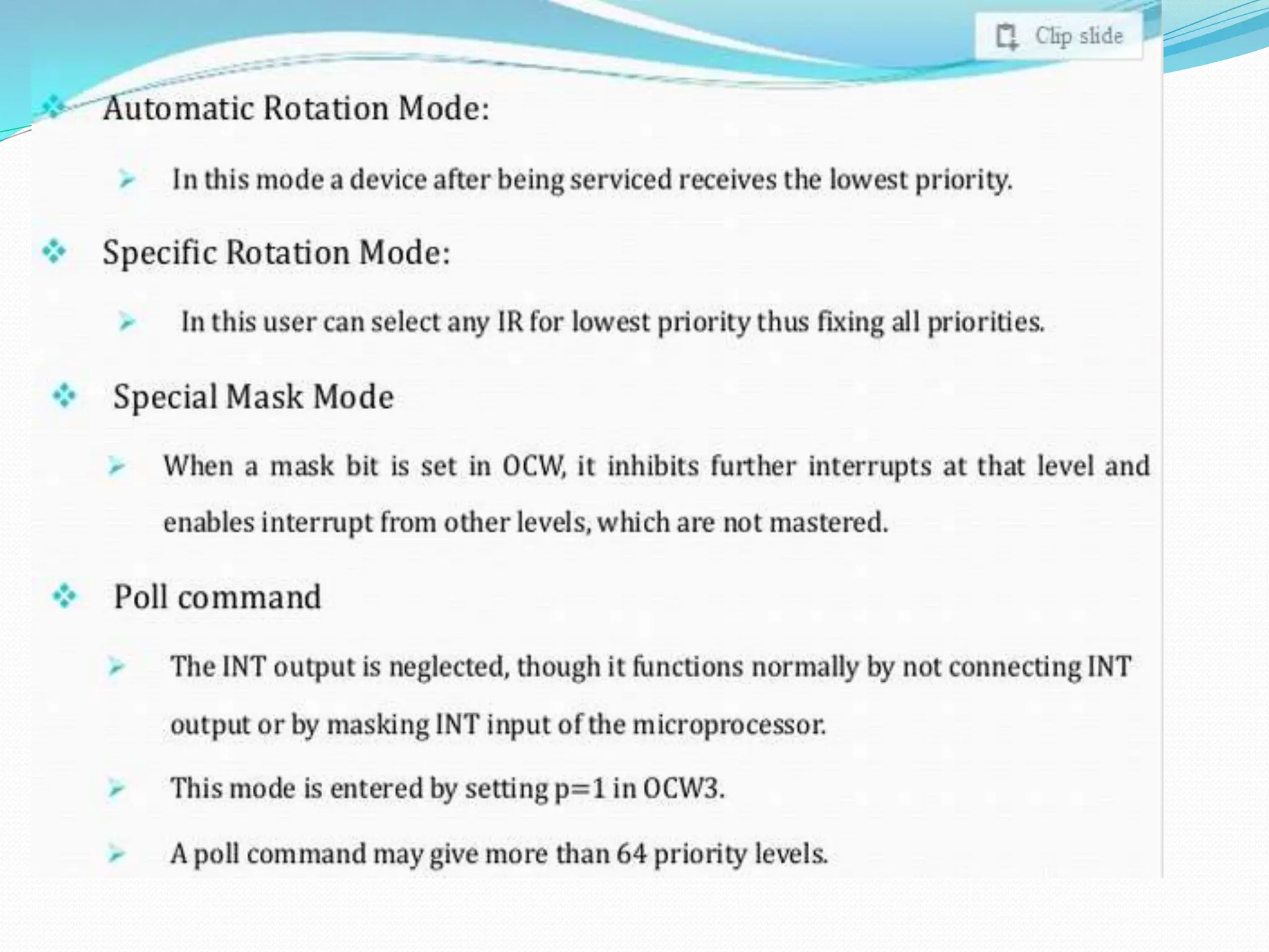
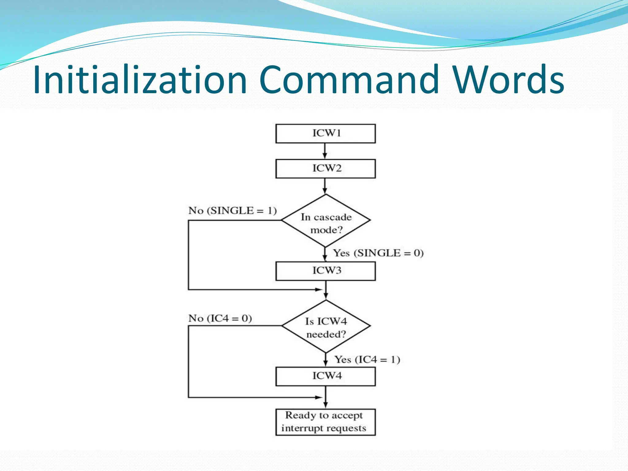
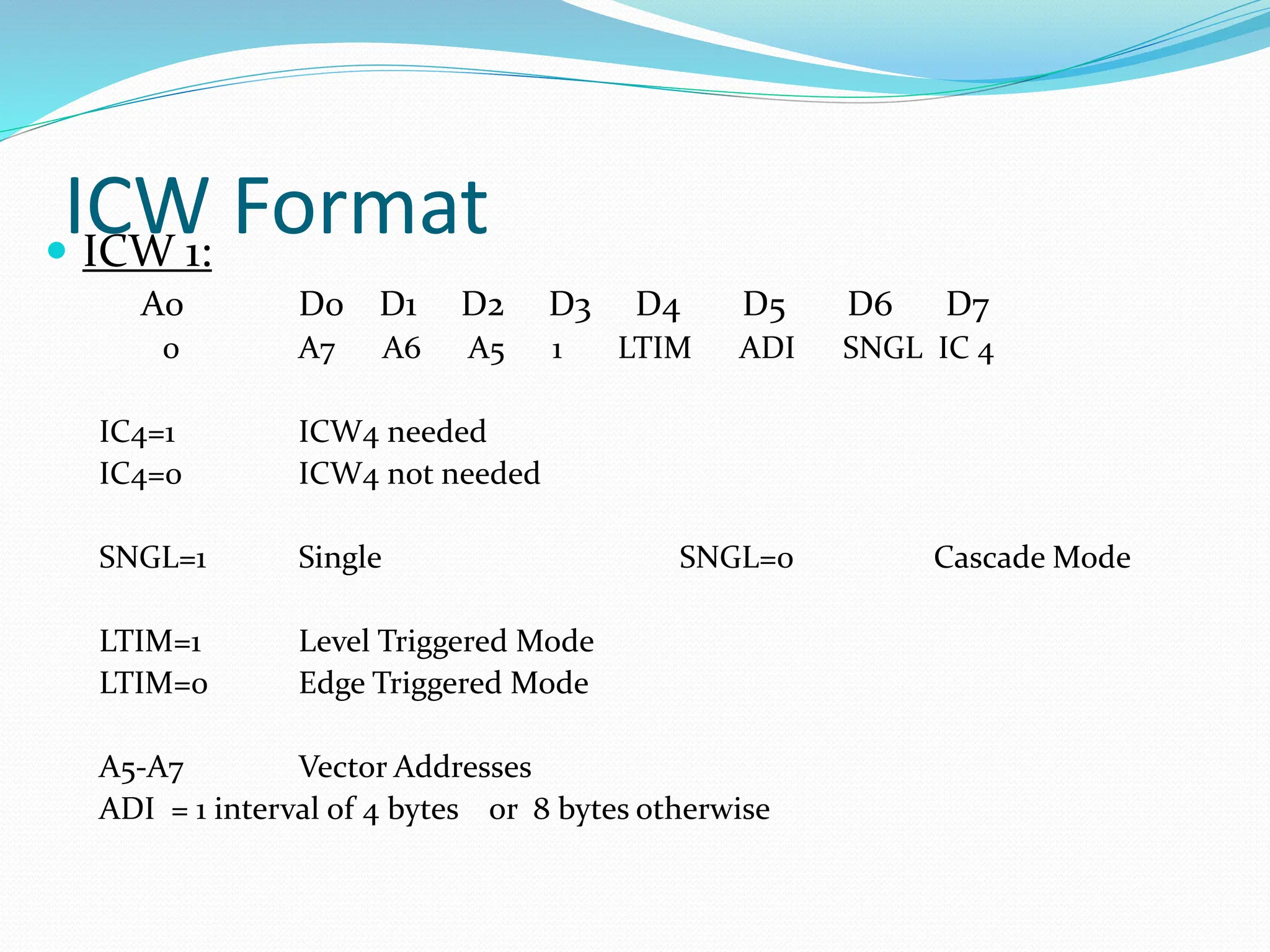
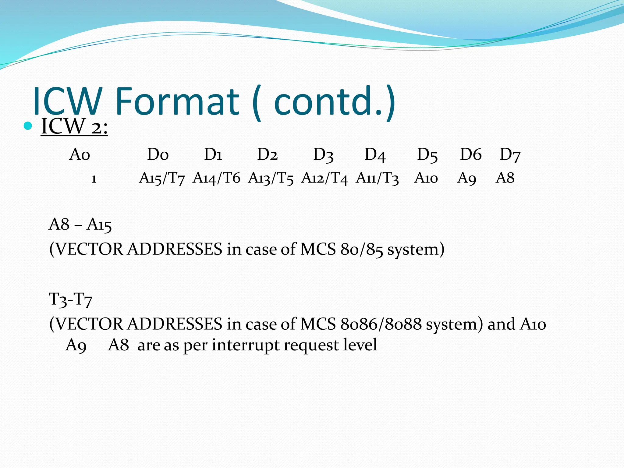
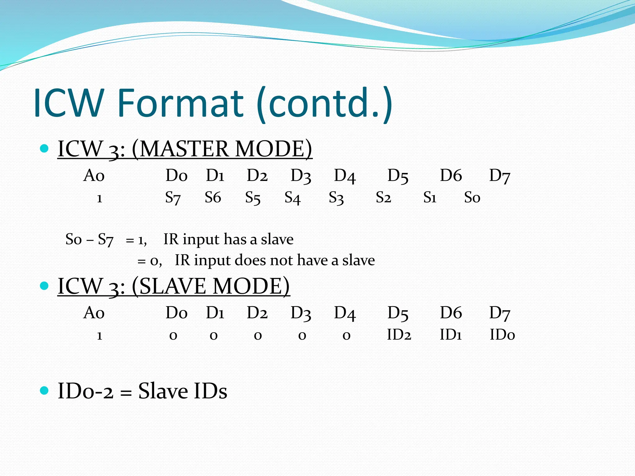
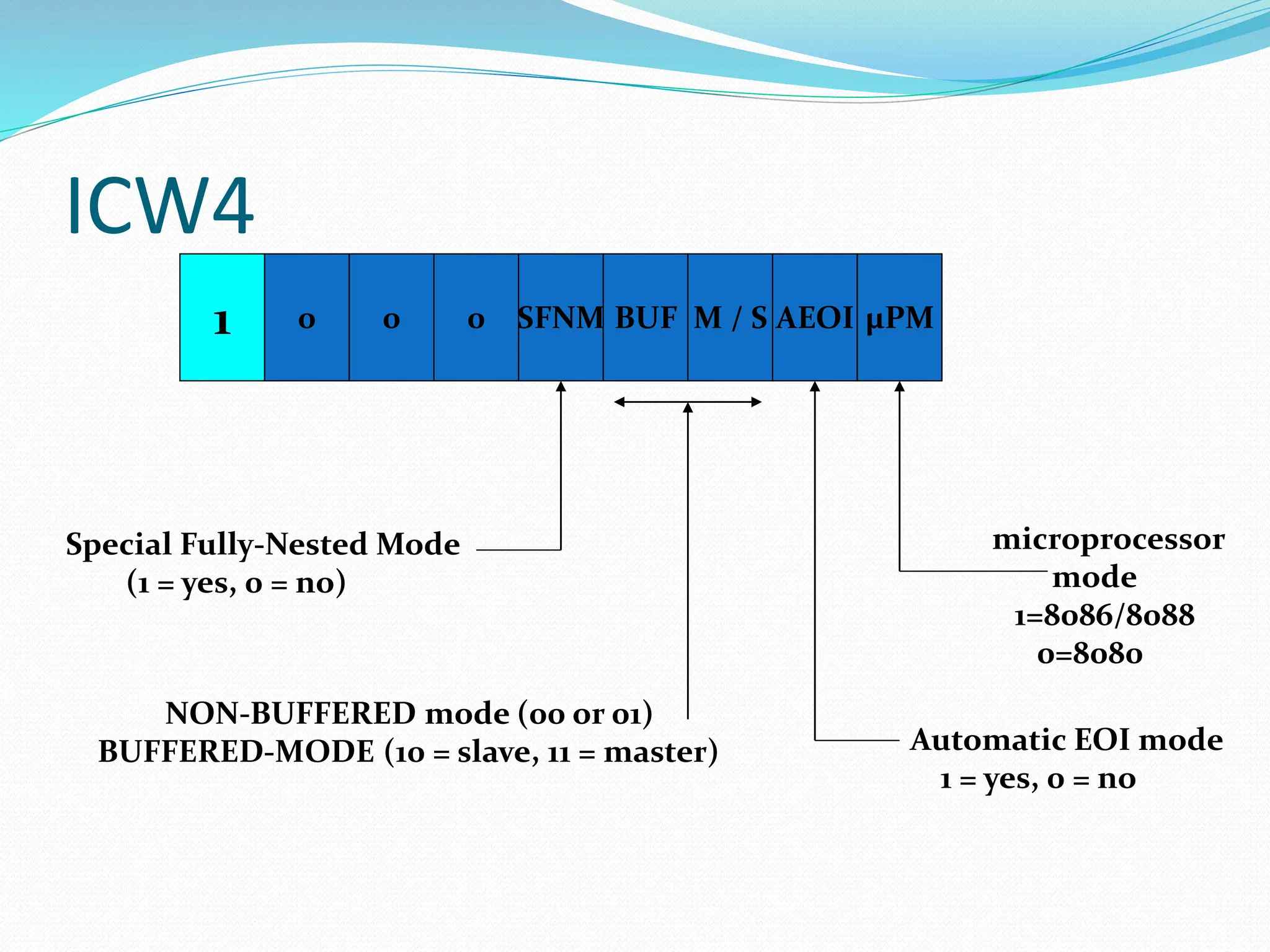
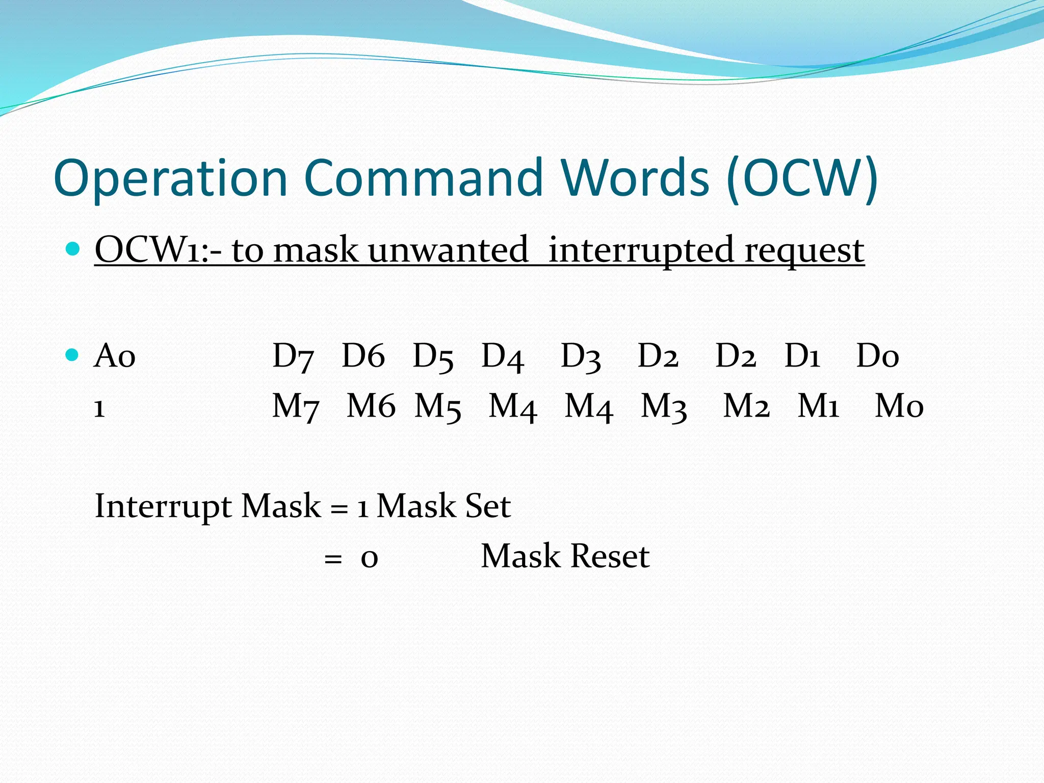
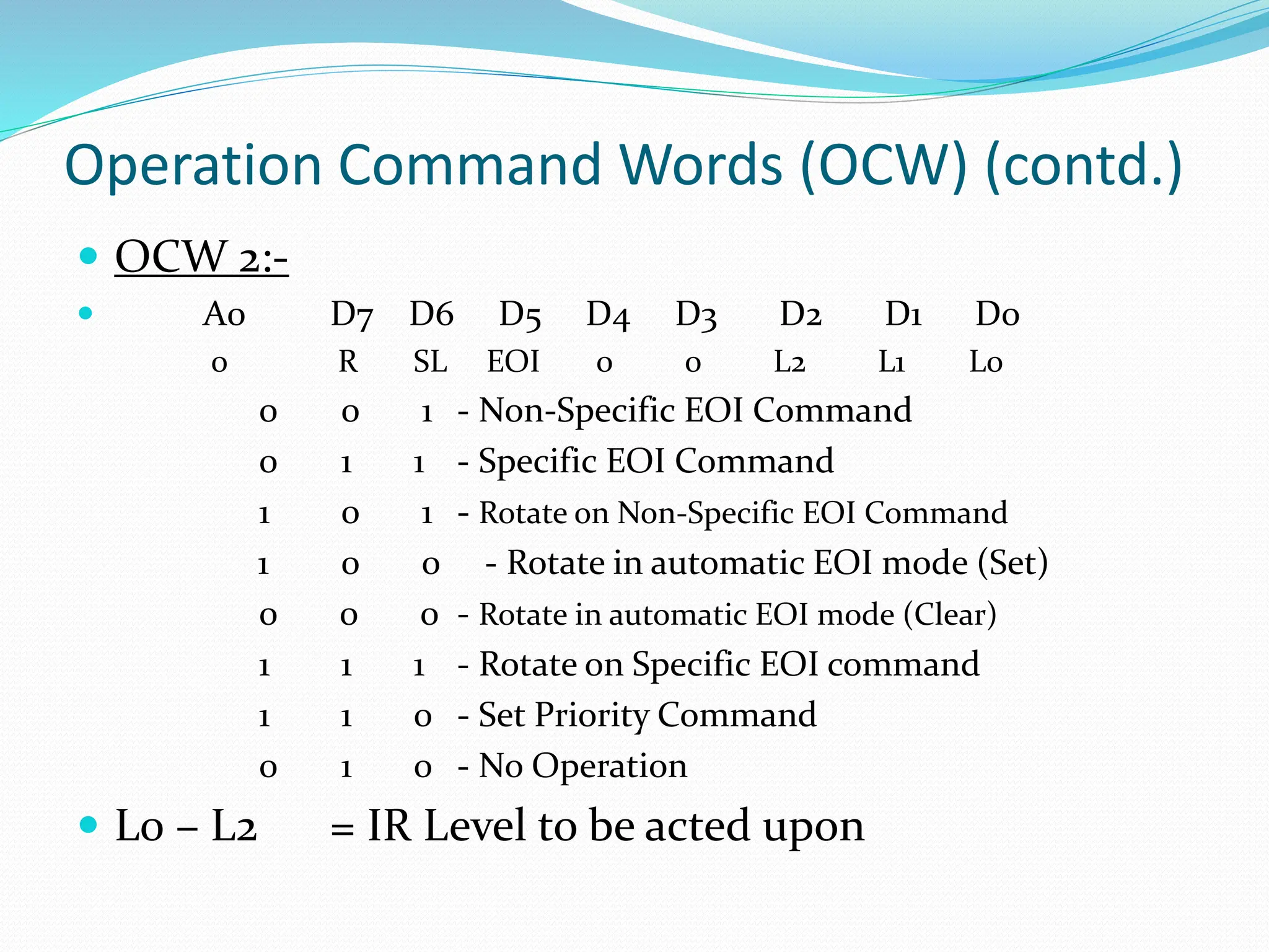
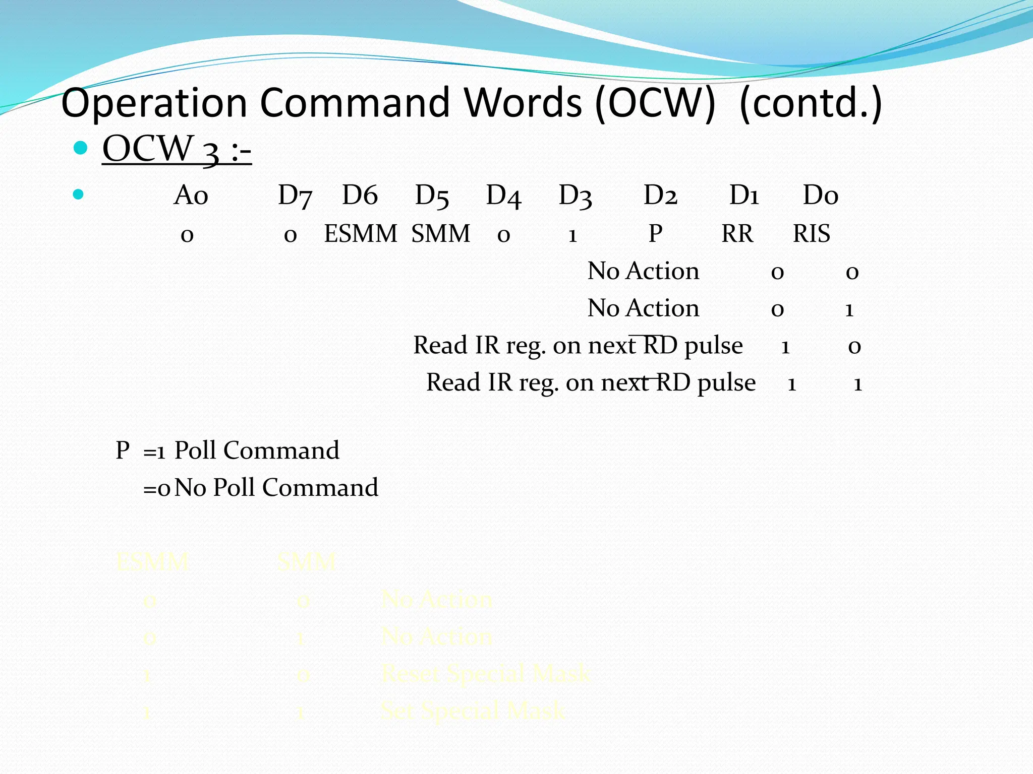
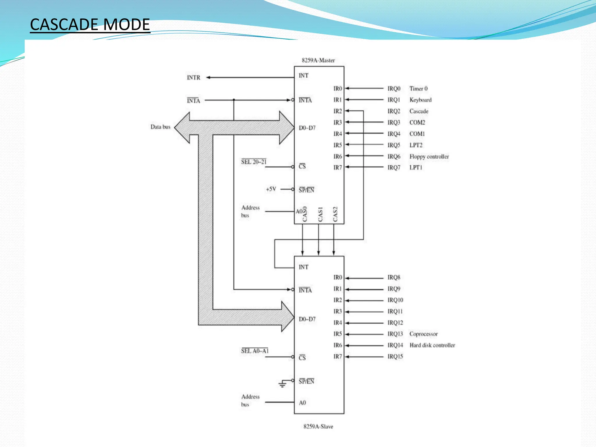
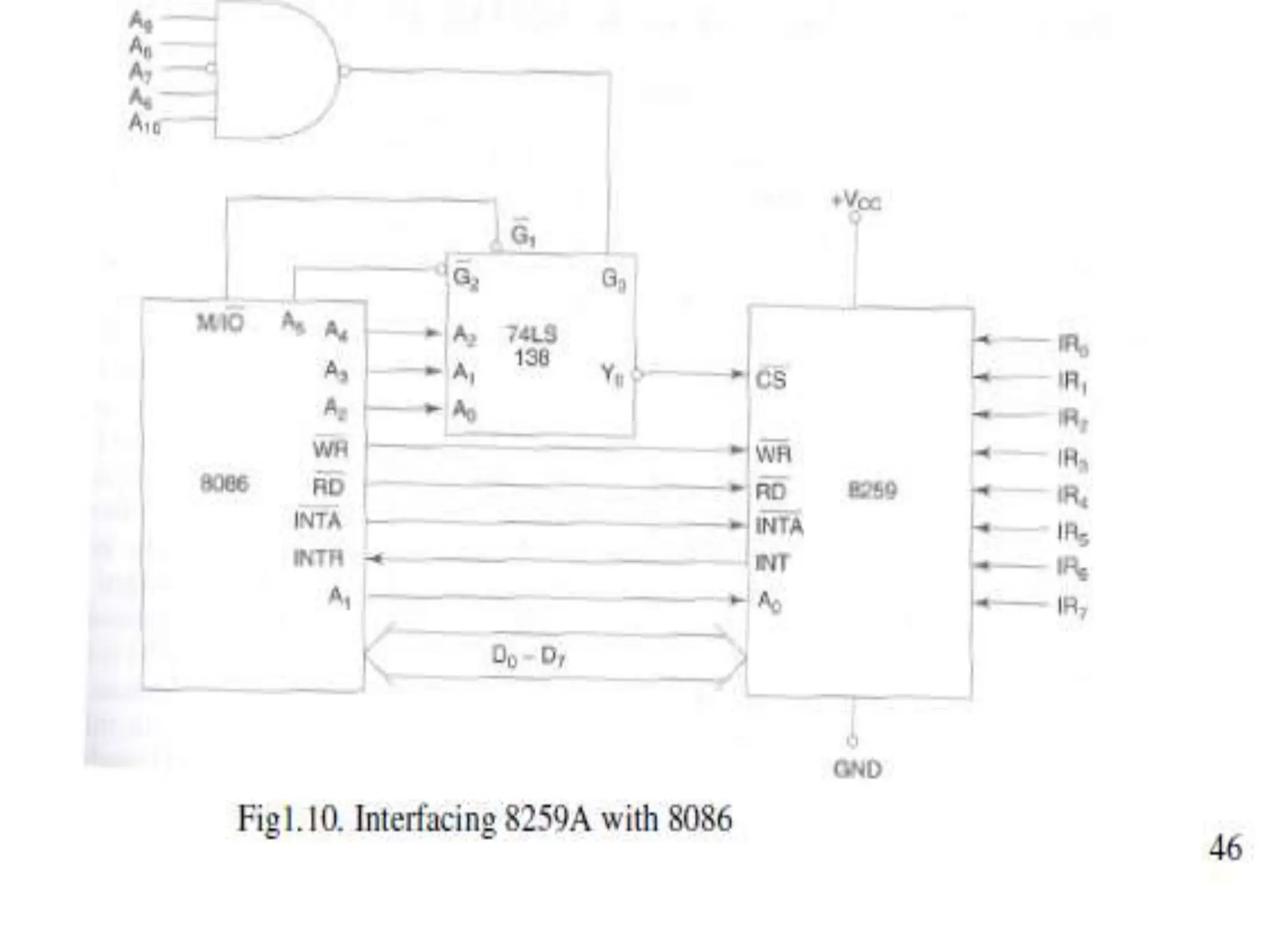
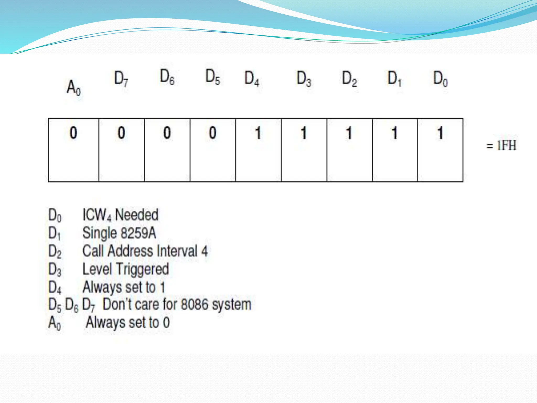
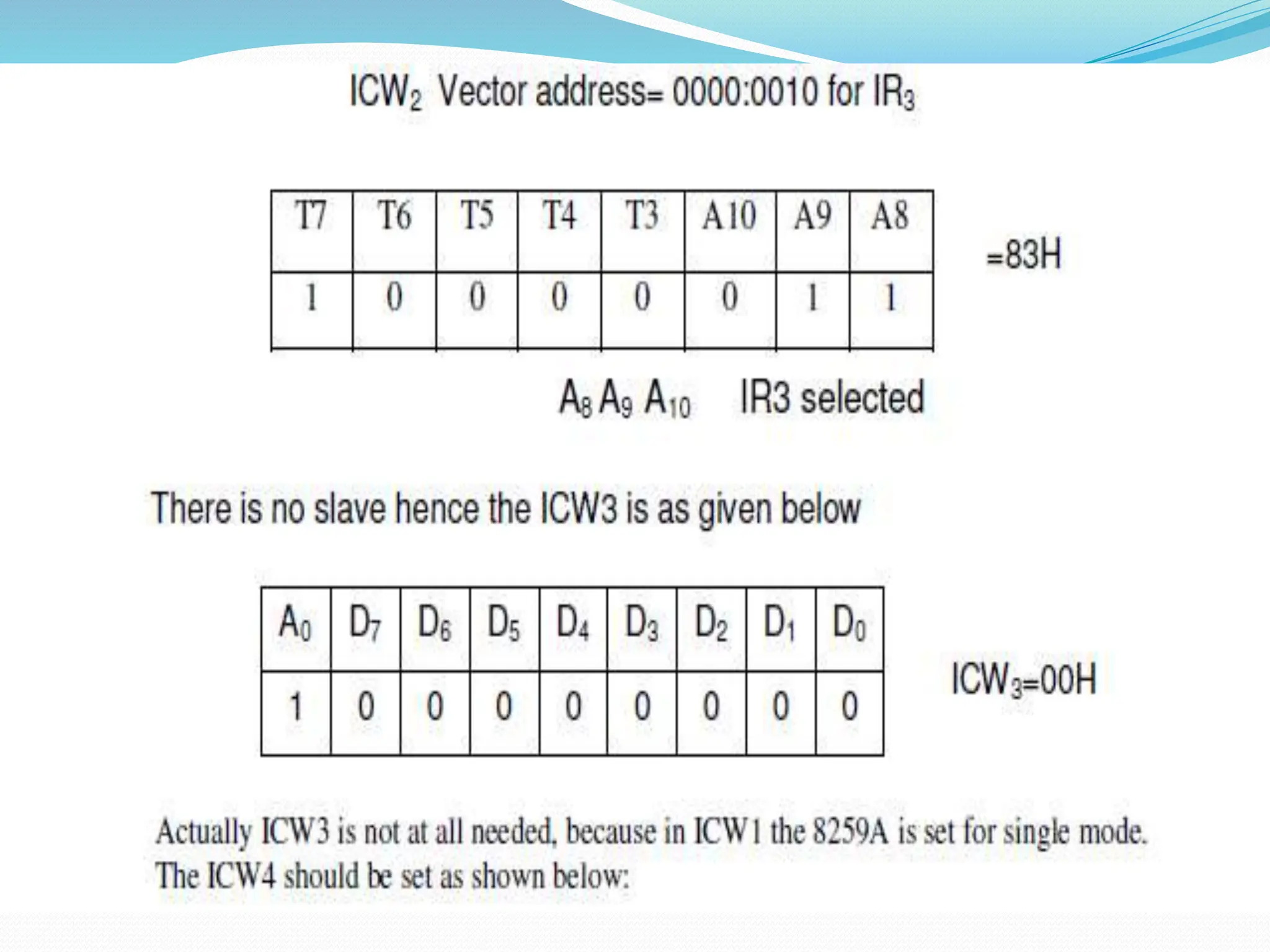
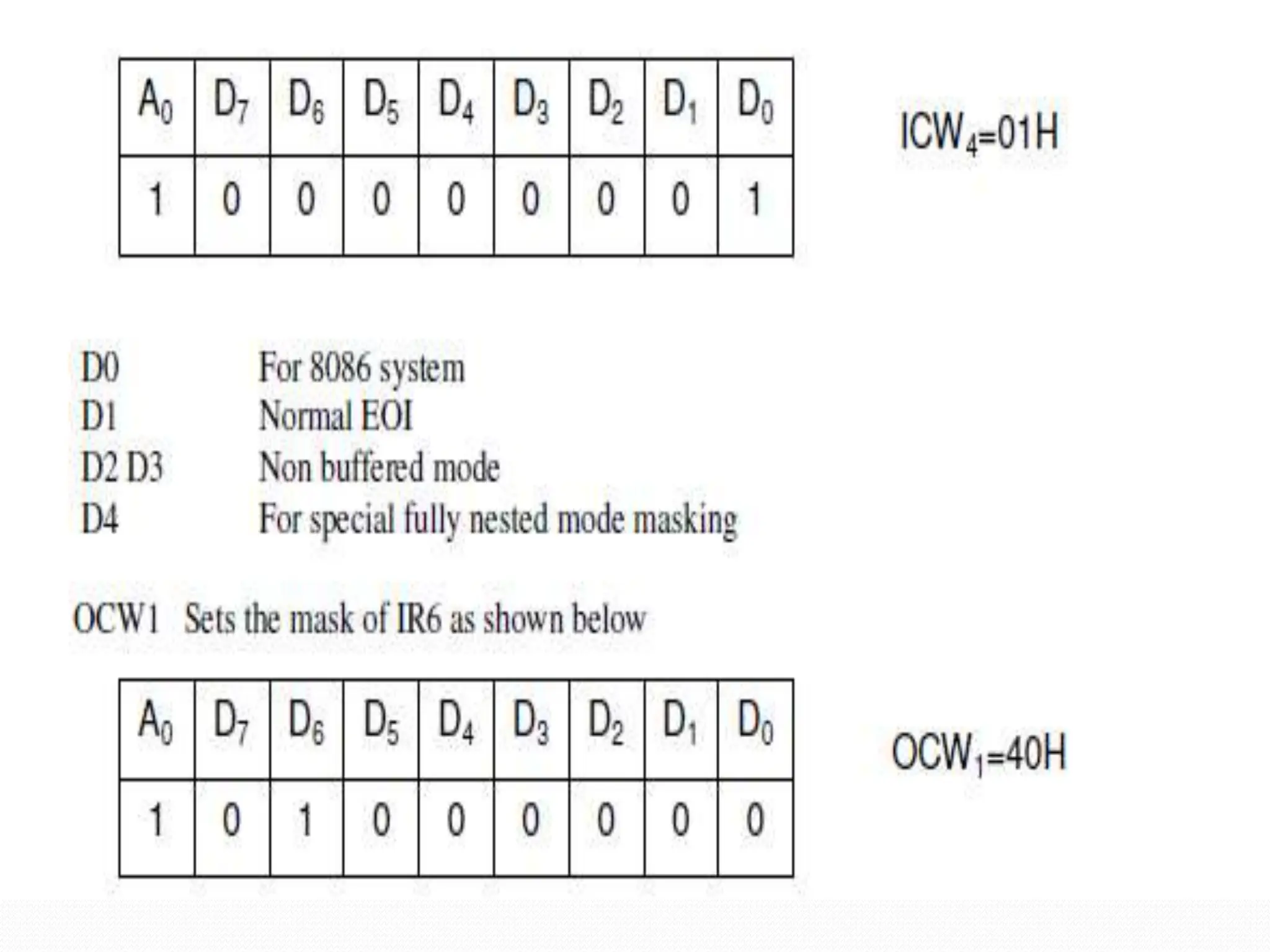
Coefficient of Thermal Expansion and their Importance.pptx
unit 2 lect 6 AND 7 8254.pptx
1.
2. Not
Possible To
Generate
Accurate
Time
Delays
Using Delay
Routines in
8086
Intel’s Programmable
Counter/ Timer Device
(8253/8254) Facilitates
• Accurate Time Delays
• Minimizes Load On Mp
• Real Time Clock
• Event Counter
• Digital One Shot
• Square Wave Generator
• Complex Waveform Generator
3. 8253
• 8253 can
operate at
frequency
from dc to
2mhz
8254-ADVANCED VERSION OF 8253
• 8254 can operate with higher clock
Frequency Range ( DC To 8 Mhz AND 10 Mhz
FOR 8254-2)
• Includes Status Read Back Command That
Latches The Count And Status Of Counters
4. Compatible with All Intel and Most other Microprocessors and Handles Inputs from DC
to 10 MHz
8 MHz 8254 and 10 MHz 8254-2
The Intel 8254 is a counter/timer device designed to solve the common timing control
problems in microcomputer system design.
It provides three independent 16-bit counters, each capable of handling clock inputs up
to 10 MHz
Binary or BCD counting
Single a +5V Supply and Standard Temperature Range
Six Programmable Counter Modes and All modes are software programmable. The 8254
is a superset of the 8253.
The 8254 uses CMOS technology and comes in a 24-pin plastic or CerDIP package.
Used for controlling real-time events such as real-time clock, events counter, and motor
speed and direction control.
5.
6.
7. Counters:
Three Counters – C1,C2 & C3
Each 16 Bit Identical Pre-settable
Down Counter Operates In BCD /Hex
Controlled By Loading Count To Command Word Register
“On The Fly” Reading
Control Logic:
CS – Logic 0 – Enables 8254
RD – Logic 0 – Tells Microprocessor Reads Count From 8254
WR – Logic 0 – Tells Microprocessor Writes Count/ Command
Into 8254
A1,A0 – Address Input Pins To Select Modes And Counters
8. Data Buffers:
8 Bit Bidirectional D0-D7 Connected To Data Bus Of Microprocessor
In Reads Data From Peripheral
Out Writes Data To Peripheral
Control Word Register:
Accepts 8 Bit Control Word Written By Microprocessor
Can Only Be Written ( Not Read)
Control Word Chooses One Of The Six Modes Of Operation
9. CS RD WR A1 A0 OPERATION
0 1 0 0 0 Write Counter 0
0 1 0 0 1 Write Counter 1
0 1 0 1 0 Write Counter 2
0 1 0 1 1 Write Control Word
0 0 1 0 0 Read Counter 0
0 0 1 0 1 Read Counter 1
0 0 1 1 0 Read Counter 2
0 0 1 1 1 No Operation ( Tristated )
0 1 1 X X No Operation ( Tristated )
1 X X X X 8254 Not Selected
12. Mode 0: Interrupt On Terminal Count
The output becomes a logic 0 when the control word is written
and remains low even after count value loaded in counter.
Counter starts decrementing after falling edge of clock
The OUT goes high upon reaching the terminal count & remains
high till reloading . OUT can be used as interrupt
13.
14. Mode 1: One-shot mode.
Monostable multivibrator
Gate input is used as trigger input
Output remains high till the count is loaded after
application of trigger, output goes low and remains low
till count becomes zero
Another count loaded, when output already low it
does not disturb counting until a new trigger is applied
at the gate
New counting starts after new trigger pulse
15.
16. Mode 2: Rate Generator / Divide by N Counter
When N is loaded as count after N pulses OUT goes low for
only one clock cycle then, count N is reloaded OUT becomes
high for N clock pulses
The number of clock pulses between the two low pulses is equal
to the count loaded
Gate logic 0 no counting
Gate logic 1 normal counting
18. Mode 3: SQUARE WAVE RATE GENERATOR
1. When count N loaded is even output remains HIGH for half
the count and LOW for the rest half of the count
2. When count N loaded is odd output remains HIGH for
(N+1)/2 and low for (N-1)/2.
3. Repeated operation gives square wave
4. Generates a continuous square-wave with Gate set to 1.
5. If count is even, 50% duty cycle otherwise OUT is high 1 cycle
longer.
20. After mode is set output goes high
When count is loaded counting down starts on reaching terminal
count output goes low for only one clock cycle, and then again
output goes HIGH
The above said low pulse can be used as a strobe for interfacing
MP with peripherals
When GATE is LOW counting is inhibited and count is latched
Mode 4: Software triggered Strobe
21.
22. Once mode is programmed and counter loaded, OUT goes HIGH
Counter starts counting after the rising edge of the trigger (GATE)
The OUTPUT goes LOW for one clock period, when the terminal count is
reached
Output will not go LOW until the counter content becomes zero
GATE is used as trigger input
Mode 5: Hardware triggered Strobe
24. Read Operations
There are three possible methods for reading the
counters:
1. a simple read operation
2. the Counter Latch Command
3. the Read-Back Command
1. Simple read operation :
The Counter which is selected with the A1, A0 inputs, the CLK
input of the selected Counter must be inhibited by using either
the GATE input or external logic.
Otherwise, the count may be in the process of changing when
it is read, giving an undefined result.
25. 2. Counter Latch Command:
SC0, SC1 bits select one of the
three counters
Two other bits, D5 and D4,
distinguish this command from a
control word
If a counter is latched and then,
some time later, latched again
before the count is read, the
second counter latch command is
ignored.
The count read will be the count
at the time the first counter latch
command was issued.
26. 3. Read-back control command:
The read-back control, word is
used, when it is necessary for the
contents of more than one
counter to be read at a same time.
Count : logic 0, select one of the
Counter to be latched
Status : logic 0, Status must be
latched to be read status of a
counter and is accessed by a
read from that counter
27. Status register:
•Shows the state of the output pin
•Check the counter is in null state (0) or not
•How the counter is programmed
28. Example : Write a program to generate a square
wave of 1KHz frequency on OUT 1 pin of 8253/54.
Assume CLK1 frequency is 1 MHz and address for
control register = 0BH, counter 1 = 09H and counter
2 = 0AH.
29.
30.
31. Example:
Design a programmable timer using 8253 and 8086. Interface
8253 at an address 0040H for counter 0 and write the following
ALPs. The 8086 and 8253 run at 6 MHz and 1.5 MHz
respectively,
1. To generate a square wave of period 1 ms.
2. To interrupt the processor after 10 ms.
3. To derive a mono shot pulse with quasi stable state
duration 5 ms.
32. Solution:
Neglecting the higher order address lines (A16-A8) the
interfacing circuit diagram is shown in Fig.
The 8253 is interfaced with lower order data bus
(D0-D7), hence A0 is used for selecting the even bank.
The A0 and A1 of the 8253 are connected with A1 and A2
of the processor.
The counter addresses can be decoded as given below.
If A0 is 1, the 8253 will not be selected at all.
33.
34.
35.
36.
37.
38.
39.
40.
41. iii.
For generating a 5ms quasi stable state
duration, the count required is calculated
first.
The counter 2 of 8253 is used in mode 1, to
count in binary.
The OUT2 signal normally remains high after
the count is loaded, till the trigger is applied.
After the application of trigger signal, the
output goes low in the next cycle, count down
starts and whenever the count goes zero the
output again goes high.
48. Interrupts in Microcomputer System
Microcomputer system design
requires I.O devices such as
keyboards, displays, sensors and
other components
I.O devices should receive servicing
in an efficient manner so that large
amounts of the total system tasks can
be done by the microcomputer with
little or no effect on throughput
49. General Method :Polled Method
The most common method of servicing such
devices is the Polled approach.
This is where the processor must test each device
in sequence and in effect ``ask'' each one if it
needs servicing.
It is easy to see that a large portion of the main
program is looping through this continuous
polling cycle and hence serious effect on system
throughput,
50. A More Reliable Method : Interrupt
the microprocessor is executing its main program and only
stop to service peripheral devices when it is told to do so by
the device itself or been interrupted.
Once this servicing is complete, however, the processor
would resume exactly where it left off
51. it ?
The Programmable Interrupt Controller (PIC) functions as an
overall manager in an Interrupt-Driven system environment.
It accepts
-requests from the peripheral equipment,
-determines which of the incoming requests is of the
highest importance (priority),
-ascertains whether the incoming request has a higher
priority value than the level currently being serviced,
- issues an interrupt to the CPU based on this
determination.
Each peripheral device has subroutine also referred to as a
service routine''.
The PIC, after issuing an Interrupt to the CPU, points the
Program Counter to the service routine associated with the
requesting device.
This pointer is an address in a vectoring table and will often be
referred to as vectoring data.
54. IRR and ISR
INTERRUPT REQUEST REGISTER (IRR) AND IN-
SERVICE REGISTER (ISR)
The interrupts at the IR input lines are handled by
two registers in cascade, the Interrupt Request
Register (IRR) and the In-Service (ISR).
The IRR is used to store all the interrupt levels
which are requesting service; and the ISR is used
to store all the interrupt levels which are being
serviced.
55. Priority Resolver
This logic block determines the priorities of the bits
set in the IRR.
The highest priority is selected and strobed into the
corresponding bit of the ISR during INTA pulse.
56. Interrupt Mask Register
The IMR stores the bits which mask the interrupt lines
to be masked. The IMR operates on the IRR.
Masking of a higher priority input will not affect the
interrupt request lines of lower quality.
57. INT(Interrupt)
This output goes directly to the CPU interrupt input.
The VOH level on this line is designed to be fully
compatible with the 8080A, 8085A and 8086 input
levels.
58. INTA(Interrupt Acknowledgement)
INTA pulses will cause the 8259A to release
vectoring information onto the data bus. The format of
this data depends on the system mode of the 8259A.
59. Data Bus Buffer
This 3-state, bidirectional 8-bit buffer is used to
interface the 8259A to the system Data Bus.
Control words and status information are transferred
through the Data Bus Buffer
60. Read-Write Control Logic
The function of this block is to accept OUTput
commands from the CPU.
It contains the Initialization Command Word
(ICW) registers and Operation Command Word
(OCW) registers which store the various control
formats for device operation.
This function block also allows the status of the
8259A to be transferred onto the Data Bus
61. Chip Select ( CS )
A LOW on this input enables the 8259A. No reading or
writing of the chip will occur unless the device is
selected
A0
This input signal is used in conjunction with WR and RD
signals to write commands into the various command
registers, as well as reading the various status registers of
the chip. This line can be tied directly to one of the address
lines
62. RD & WR
A LOW on WR input enables the CPU to write control
words (ICWs and OCWs) to the 8259A.
A LOW on RD input enables the 8259A to send the
status of the Interrupt Request Register (IRR), In
Service Register (ISR), the Interrupt Mask Register
(IMR), or the Interrupt level onto the Data Bus.
64. The Cascade Buffer/Comparator
This function block stores and compares the IDs of
all 8259A's used in the system. The associated
three I/O pins (CAS0-2) are outputs when the
8259A is used as a master and are inputs when the
8259A is used as a slave.
As a master, the 8259A sends the ID of the
interrupting slave device onto the CAS 0-2 lines.
The slave thus selected will send its
preprogrammed subroutine address onto the Data
Bus during the next one or two consecutive INTA
pulses.
65. INTERRUPT SEQUNCE
The events occur as follows in an MCS-80/85 system:
1. One or more of the INTERRUPT REQUEST lines (IR7-0) are
raised high, setting the corresponding IRR bit (s).
2. The 8259A evaluates these requests, and sends an INT to the
CPU, if appropriate.
3. The CPU acknowledges the INT and responds with an INTA
pulse.
4. Upon receiving an INTA from the CPU group, the highest
priority ISR bit is set, and the corresponding IRR bit is reset. The
8259A will also release a CALL instruction code (11001101) onto the
8-bit Data Bus through its D0-D7 pins.
5. This CALL instruction will initiate two more INTA pulses to be
sent to the 8259A from the CPU group.
6. These two INTA pulses allow the 8259A to release its
preprogrammed subroutine address onto the Data Bus. The
lower 8-bit address is released at the first INTA pulse and the
higher 8-bit address is released at the second INTA pulse.
7. This completes the 3-byte CALL instruction released by the
8259A. In the AEOI mode the ISR bit is reset at the end of the
third INTA pulse. Otherwise, the ISR bit remains set until an
appropriate EOI command is issued at the end of the interrupt
67. Interrupt Sequence Outputs
This sequence is timed by three INTA pulses. During the first INTA
pulse the CALL opcode is enabled onto the data bus.
Content of First Interrupt Vector Byte -
D7 D6 D5 D4 D3 D2 D1 D0
1 1 0 0 1 1 0 1
During the second INTA pulse the lower address of the appropriate
service routine is enabled onto the data bus. When Interval = 4 bits A5-
A7 are programmed, while A0-A4 are automatically inserted by the
8259A.
When Interval = 8 only A6 and A7 are programmed, while A0-A5 are
automatically inserted.
69. Interrupt Sequence Outputs (Contd.)
During the third INTA pulse the higher address of the
appropriate service routine, which was programmed
as byte 2 of the initialization sequence (A8-A15), is
enabled onto the bus.
Content of Third Interrupt Vector Byte
D7 D6 D5 D4 D3 D2 D1 D0
A15 A14 A13 A12 A11 A10 A9 A8
70. The interrupt sequence in an 8086-8259A system is
described as follows:
1. One or more IR lines are raised high that set
corresponding IRR bits.
2. 8259A resolves priority and sends an INT signal to CPU.
3. The CPU acknowledges with INTA pulse.
4. Upon receiving an INTA signal from the CPU, the
highest priority ISR bit is set and the corresponding IRR bit
is reset. The 8259A does not drive data bus during this
period.
5. The 8086 will initiate a second INTA pulse. During this
period 8259A releases an 8-bit pointer on to data bus from
where it is read by the CPU.
6. This completes the interrupt cycle. The ISR bit is reset at
the end of the second INTA pulse if automatic end of
interrupt (AEOI) mode is programmed. Otherwise ISR bit
remains set until an appropriate EOI command is issued at
the end of interrupt subroutine.
71. PROGRAMMING THE 8259A
The 8259A accepts two types of command words generated by the CPU:
1. Initialization Command Words (ICWs): as good as CWR
2. Operation Command Words (OCWs): These are the command
words which command the 8259Ato operate in various interrupt
modes.
These modes are:
a. Fully nested mode
b. Rotating priority mode
c. Special mask mode
d. Polled mode
The OCWs can be written into the 8259A anytime after initialization.
80. Operation Command Words (OCW) (contd.)
OCW 2:-
A0 D7 D6 D5 D4 D3 D2 D1 D0
0 R SL EOI 0 0 L2 L1 L0
0 0 1 - Non-Specific EOI Command
0 1 1 - Specific EOI Command
1 0 1 - Rotate on Non-Specific EOI Command
1 0 0 - Rotate in automatic EOI mode (Set)
0 0 0 - Rotate in automatic EOI mode (Clear)
1 1 1 - Rotate on Specific EOI command
1 1 0 - Set Priority Command
0 1 0 - No Operation
L0 – L2 = IR Level to be acted upon
81. Operation Command Words (OCW) (contd.)
OCW 3 :-
A0 D7 D6 D5 D4 D3 D2 D1 D0
0 0 ESMM SMM 0 1 P RR RIS
No Action 0 0
No Action 0 1
Read IR reg. on next RD pulse 1 0
Read IR reg. on next RD pulse 1 1
P =1 Poll Command
=0No Poll Command
ESMM SMM
0 0 No Action
0 1 No Action
1 0 Reset Special Mask
1 1 Set Special Mask
82. OCW Description :-
OCW 3 :-
ESMM (Enable Special Mask Mode) - When this bit is set
to 1 it enables the SMM bit to set or reset the Special Mask
Mode. When ESMM e 0 the SMM bit becomes a ``don't
care''.
SMM (Special Mask Mode) - If ESMM = 1 and SMM = 1 the
8259A will enter Special Mask Mode. If ESMM = 1 and
SMM = 0 the 8259A will revert to normal mask mode.
When ESMM = 0, SMM has no effect.
83. Fully Nested Mode
This mode is entered after initialization unless another mode is
programmed. The interrupt requests are ordered in priority from 0
through 7 (0 highest). When an interrupt is acknowledged the highest
priority request is determined and its vector placed on the bus.
Additionally, a bit of the Interrupt Service register (ISO-7) is set. This
bit remains set until the microprocessor issues an End of Interrupt
(EOI) command immediately before returning from the service
routine, or if AEOI (Automatic End of Interrupt) bit is set, until the
trailing edge of the last INTA. While the IS bit is set, all further
interrupts of the same or lower priority are inhibited, while higher
levels will generate an interrupt (which will be acknowledged only if
the microprocessor internal Interrupt enable flip-flop has been re-
enabled through software).
After the initialization sequence, IR0 has the highest prioirity and IR7
the lowest. Priorities can be changed, as will be explained, in the
rotating priority mode.
84. EOI (End Of Interrupt)
The In Service (IS) bit can be reset either automatically following the trailing
edge of the last in sequence INTA pulse (when AEOI bit in ICW1 is set) or by a
command word that must be issued to the 8259A before returning from a service
routine (EOI command). An EOI command must be issued twice if in the Cascade
mode, once for the master and once for the corresponding slave.
There are two forms of EOI command: Specific and Non-Specific. When the 8259A
is operated in modes which preserve the fully nested structure, it can determine
which IS bit to reset on EOI. When a Non-Specific EOI command is issued the
8259A will automatically reset the highest IS bit of those that are set, since in the
fully nested mode the highest IS level was necessarily the last level acknowledged
and serviced. A non-specific EOI can be issued with OCW2 (EOI = 1, SL = 0, R = 0).
When a mode is used which may disturb the fully nested structure, the 8259A may
no longer be able to determine the last level acknowledged.
In this case a Specific End of Interrupt must be issued which includes as part of
the command the IS level to be reset.
A specific EOI can be issued with OCW2 (EOI =1, SL=1, R= 0, and L0-L2 is the
binary level of the IS bit to be reset).
It should be noted that an IS bit that is masked by an IMR bit will not be cleared
by a non-specific EOI if the 8259A is in the Special Mask Mode.
85. Automatic End of Interrupt (AEOI)
Mode
If AEOI =1 in ICW4, then the 8259A will operate in AEOI
mode continuously until reprogrammed by ICW4 , in
this mode the 8259A will automatically perform a non-
specific EOI operation at the trailing edge of the last
interrupt acknowledge pulse (third pulse in MCS-80/85,
second in 8086).
Note that from a system standpoint, this mode should
be used only when a nested multilevel interrupt
structure is not required within a single 8259A.
The AEOI mode can only be used in a master 8259A
and not a slave. 8259As with a copyright date of 1985 or
later will operate in the AEOI mode as a master or a
slave.
86. AUTOMATIC ROTATION
In some applications there are a number of interrupting devices of equal priority.
In this mode a device, after being serviced, receives the lowest priority, so a device
requesting an interrupt will have to wait, in the worst case until each of 7 other
devices are serviced at most once . For example, if the priority and ``in service''
status is:
Before Rotate (IR4 the highest priority requiring service) :-
IS7 IS6 IS5 IS4 IS3 IS2 IS1 IS0
0 1 0 1 0 0 0 0 IS STATUS
7 6 5 4 3 2 1 0 Priority Status
After Rotate (IR4 the highest priority requiring service) :-
IS7 IS6 IS5 IS4 IS3 IS2 IS1 IS0
0 1 0 0 0 0 0 0 IS STATUS
2 1 0 7 6 5 4 3 Priority Status
87. Specific Rotation (Specific Priority)
The programmer can change priorities by programming the bottom
priority and thus fixing all other priorities ;i.e., if IR5 is programmed as
the bottom priority device, then IR6 will have the highest one.
The Set Priority command is issued in OCW2 where: R=1, SL=1, L0-L2
is the binary priority level code of the bottom priority device.
Observe that in this mode internal status is updated by software
control during OCW2.
However, it is independent of the End of Interrupt (EOI) command
(also executed by OCW2).
Priority changes can be executed during an EOI command by using the
Rotate on Specific EOI command in OCW2 (R=1, SL=1, EOI=1 and LO-
L2 IR level to receive bottom priority).
88. INTERRUPT MASK
Each Interrupt Request input can bem masked individually by the Interrupt
Mask Register (IMR) programmed through OCW1. Each bit in the IMR masks one
interrupt channel if it is set (1). Bit 0 masks IR0,Bit 1 masks IR1 and so forth.
Masking an IR channel does not affect the other channels operation.
SPECIAL MASK MODE
Some applications may require an interrupt service routine to dynamically
alter the system priority structure during its execution under software control.
For example, the routine may wish to inhibit lower priority requests for a
portion of its execution but enable some of them for another portion.
The difficulty here is that if an Interrupt Request is acknowledged and an End
of Interrupt command did not reset its IS bit (i.e., while executing a service
routine), the 8259A would have inhibited all lower priority requests with no
easy way for the routine to enable them. That is where the Special Mask Mode
comes in. In the special Mask Mode, when a mask bit is set in
OCW1, it inhibits further interrupts at that level and Enables interrupts from
all other levels (lower as well as higher) that are not masked. Thus, any
interrupts may be selectively enabled by loading the mask register.
The special Mask Mode is set by OWC3 where:
SSMM =1, SMM =1, and cleared where SSMM =1, SMM = 0.
89. POLL COMMAND
In Poll mode the INT output functions as it normally does. The microprocessor
should ignore this output. This can be accomplished either by not connecting
the INT output or by masking interrupts within the microprocessor, thereby
disabling its interrupt input. Service to devices is achieved by software using a
Poll command. The Poll command is issued by setting P = `1'' in OCW3. The
8259A treats the next RD pulse to the 8259A (i.e., RD e 0, CS e 0) as an
interrupt acknowledge, sets the appropriate IS bit if there is a request, and
reads the priority level. Interrupt is frozen from WR to RD. The word enabled
onto the data bus during RD is:
D7 D6 D5 D4 D3 D2 D1 D0
I - - - - w2 w1 w0
W0 - W2: Binary code of the highest priority level requesting service.
I : Equal to ``1'' if there is an interrupt.
This mode is useful if there is a routine command common to several levels so
that the INTA sequence is not needed (saves ROM space). Another application
is to use the poll mode to expand the number of priority levels to more than 64.
91. CASCADE MODE (contd.)
The 8259A can be easily interconnected in a system of one master with up to eight
slaves to handle up to 64 priority levels.
The master controls the slaves through the 3 line cascade bus. The cascade bus
acts like chip selects to the slaves during the INTA sequence.
In a cascade configuration, the slave interrupt outputs are connected to the
master interrupt request inputs. When a slave request line is activated and
afterwards acknowledged, the master will enable the corresponding slave to
release the device routine address during bytes 2 and 3 of INTA. (Byte 2 only for
8086/8088).
The cascade bus lines are normally low and will contain the slave address code
from the trailing edge of the first INTA pulse to the trailing edge of the third
pulse. Each 8259A in the system must follow a separate initialization sequence
and can be programmed to work in a different mode. An EOI command must be
issued twice: once for the master and once for the corresponding slave. An
address decoder is required to activate the Chip Select (CS) input of each 8259A.
The cascade lines of the Master 8259A are activated only for slave inputs, non-
slave inputs leave the cascade line inactive (low).
92. Remaining Topics:-
Reading Status Registers:-
The input status of several internal registers can be read to update
the user information on the system.
Edge & Level Triggered Modes:-
This mode is programmed using bit 3 in ICW1.If LTIM e `0', an interrupt
request will be recognized by a low to high transition on an IR input. The
IR input can remain high without generating another interrupt.
If LTIM =‘1', an interrupt request will be recognized by a `high' level on
IR Input, and there is no need for an edge detection. The interrupt
request must be removed before the EOI command is issued or the CPU
interrupts is enabled to prevent a second interrupt from occurring.
93. The Special Fully Nested Mode
This mode will be used in the case of a big system where cascading is used, and
the priority has to be conserved within each slave. In this case the fully nested
mode will be programmed to the master (using ICW4). This mode is similar to
the normal nested mode with the following exceptions:
A) When an interrupt request from a certain slave is in service this slave is not
locked out from the master's priority logic and further interrupt requests from
higher priority IR's within the slave will be recognized by the master and will
initiate interrupts to the processor. (In the normal nested mode a slave is
masked out when its request is in service and no higher requests from the same
slave can be serviced.)
B) When exiting the Interrupt Service routine the software has to check
whether the interrupt serviced was the only one from that slave. This is done by
sending a non-specific End of Interrupt (EOI) command to the slave and then
reading its In-Service register and checking for zero. If it is empty, a non-
specific EOI can be sent to the master too. If not, no EOI should be sent.
94. Buffered Mode
When the 8259A is used in a large system where bus
driving buffers are required on the data bus and the
cascading mode is used, there exists the problem of
enabling buffers.
The buffered mode will structure the 8259A to send an
enable signal on SP/EN to enable the buffers. In this mode,
whenever the 8259A's data bus outputs are enabled, the
SP/EN output becomes active.
This modification forces the use of software programming
to determine whether the 8259A is a master or a slave. Bit 3
in ICW4 programs the buffered mode, and bit 2 in ICW4
determines whether it is a master or a slave.
95. Interfacing and programming 8259
Example:
Show 8259A interfacing connections with 8086 at the address
074x. Write an ALP to initialize the 8259A in single level triggered
mode. Then set the 8259A to operate with IR6 masked, IR4 as
bottom priority level, with special EOI mode. Set special mask
mode of 8259A. Read IRR and ISR into registers BH and BL
respectively.
96. Let the starting address is 0000:0010. The interconnections of
8259A with 8086 are as shown in coming slides
The 8259 is interfaced with lower byte of the 8086 data bus, hence
A0 line of the microprocessor system is abandoned and A1 of the
microprocessor system is connected with A0 of the 8259A.
Before going for an ALP, all the initialization command words
(ICWS) and Operation command word (OCWS) must be decided.
ICW1 decides single level triggered, address interval of 4 as given
below.
97.
98.
99.
100.
101.
102.
103.
104.
105. Features:
It is a 4-channel DMA.
So 4 I/O devices can be interfaced to DMA
It is designed by Intel
Each channel have 16-bit address and 14 bit counter
It provides chip priority resolver that resolves priority of
channels in fixed or rotating mode.
It provide on chip channel inhibit logic.
106. It generates a TC signal to indicate
the peripheral that the
programmed number of data bytes
have been transferred.
It generates MARK signal to
indicate the peripheral that 128
bytes have been transferred.
It requires single phase clock.
The maximum frequency is 3Mhz
and minimum frequency is 250 Hz.
107. It execute 3 DMA cycles
1.DMA read 2.DMA write 3.DMA
verify.
It provide AEN signal that can be
used to isolate CPU and other devices
from the system bus.
It is operate in two modes.
1.Master Mode
2.Slave Mode
109. Description of pin diagram
D0-D7:
it is a bidirectional ,tri state ,Buffered ,Multiplexed
data (D0-D7)and (A8-A15).
In the slave mode it is a bidirectional (Data is moving).
In the Master mode it is a unidirectional (Address is
moving).
110. IOR:
It is active low ,tristate ,buffered ,Bidirectional lines.
In the slave mode it function as a input line. IOR signal is
generated by microprocessor to read the contents 8257
registers.
In the master mode it function as a output line. IOR
signal is generated by 8257 during write cycle
111. IOW:
It is active low ,tristate ,buffered ,Bidirectional control
lines.
In the slave mode it function as a input line. IOR signal
is generated by microprocessor to write the contents
8257 registers.
In the master mode it function as a output line. IOR
signal is generated by 8257 during read cycle
112. CLK:
It is the input line ,connected with TTL clock generator.
This signal is ignored in slave mode.
RESET:
Used to clear mode set registers and status registers
A0-A3:
These are the tristate, buffer, bidirectional address lines.
In slave mode ,these lines are used as address inputs lines
and internally decoded to access the internal registers.
In master mode, these lines are used as address outputs
lines,A0-A3 bits of memory address on the lines.
113. CS:
It is active low, Chip select input line.
In the slave mode, it is used to select the chip.
In the master mode, it is ignored.
A4-A7:
These are the tristate, buffer, output address lines.
In slave mode ,these lines are used as address outputs lines.
In master mode, these lines are used as address outputs
lines,A0-A3 bits of memory address on the lines.
114. READY:
It is a asynchronous input line.
In master mode,
When ready is high it is received the signal.
When ready is low, it adds wait state between S1 and S3
In slave mode ,this signal is ignored.
HRQ:
It is used to receiving the hold request signal from the
output device.
115. HLDA:
It is acknowledgment signal from microprocessor.
MEMR:
It is active low ,tristate ,Buffered control output line.
In slave mode, it is tristated.
In master mode ,it activated during DMA read cycle.
MEMW:
It is active low ,tristate ,Buffered control input line.
In slave mode, it is tristated.
In master mode ,it activated during DMA write cycle.
116. AEN (Address enable):
It is a control output line.
In master mode ,it is high
In slave mode ,it is low
Used it isolate the system address ,data ,and control
lines.
ADSTB: (Address Strobe)
It is a control output line.
Used to split data and address line.
It is working in master mode only.
In slave mode it is ignore.
117. TC (Terminal Count):
It is a status of output line.
It is activated in master mode only.
It is high ,it selected the peripheral.
It is low ,it free and looking for a new peripheral.
MARK:
It is a modulo 128 MARK output line.
It is activated in master mode only.
It goes high ,after transferring every 128 bytes of data
block.
118. DRQ0-DRQ3(DMA Request):
These are the asynchronous peripheral request input
signal.
The request signals is generated by external peripheral
device.
DACK0-DACK3:
These are the active low DMA acknowledge output lines.
Low level indicate that ,peripheral is selected for giving
the information (DMA cycle).
In master mode it is used for chip select.
120. Description
It containing Five main Blocks.
1. Data bus buffer
2. Read/Control logic
3. Control logic block
4. Priority resolver
5. DMA channels.
121. DATA BUS BUFFER:
It contain tristate ,8 bit bi-directional buffer.
Slave mode ,it transfer data between microprocessor and
internal data bus.
Master mode ,the outputs A8-A15 bits of memory address
on data lines (Unidirectional).
READ/CONTROL LOGIC:
It control all internal Read/Write operation.
Slave mode ,it accepts address bits and control signal
from microprocessor.
Master mode ,it generate address bits and control signal.
122. Control logic block:
It contains ,
1. Control logic
2. Mode set register and
3. Status Register.
CONTROL LOGIC:
Master mode ,It control the sequence of DMA
operation during all DMA cycles.
It generates address and control signals.
It increments 16 bit address and decrement 14 bit
counter registers.
It activate a HRQ signal on DMA channel Request.
Slave ,mode it is disabled.
123. MODE SET REGISTERS:
It is a write only registers.
It is used to set the operating modes.
This registers is programmed after initialization of
DMA channel.
D7 D6 D5 D4 D3 D2 D1 D0
AL TCS EW RP EN3 EN2 EN1 EN0
126. STATUS REGISTERS:
It is read only registers.
It is tell the status of DMA channels
TC status bits are set when TC signal is activated
for that channel.
Update flag is not affected during read operation.
The UP bit is set during update cycle . It is cleared
after completion of update cycle.
D7 D6 D5 D4 D3 D2 D1 D0
0 0 0 UP TC3 TC2 TC1 TCO
128. TC1=1=TC activated CH-1
TC1=0=TC activated CH-1
TC0=1=TC activated CH-0
TC0=0=TC activated CH-0
The address of status register is A3A2A1A0=1000.
FIRST/LAST FLIP FLOP:
8257 have 8bit data line and 16 bit address line.
8085 it is getting 8-bit data in simultaneously.
8085 can not access 16-bit address in simultaneously.
129. A0-A3 lines are used to distinguish between registers
,but they are not distinguish lower and higher address.
It is reset by external RESET signal.
It is also reset by whenever mode set register is loaded.
So program initialization with a dummy (00 H).
FF=1=Higher byte of address
FF=0=Lower byte of address.
130. Modes of Operation
Rotating priority Mode:
The priority of the channels has a circular sequence.
Fixed Priority Rotating Mode:
The priority is fixed.
TC Stop Mode
Auto Load mode
Extended Write mode