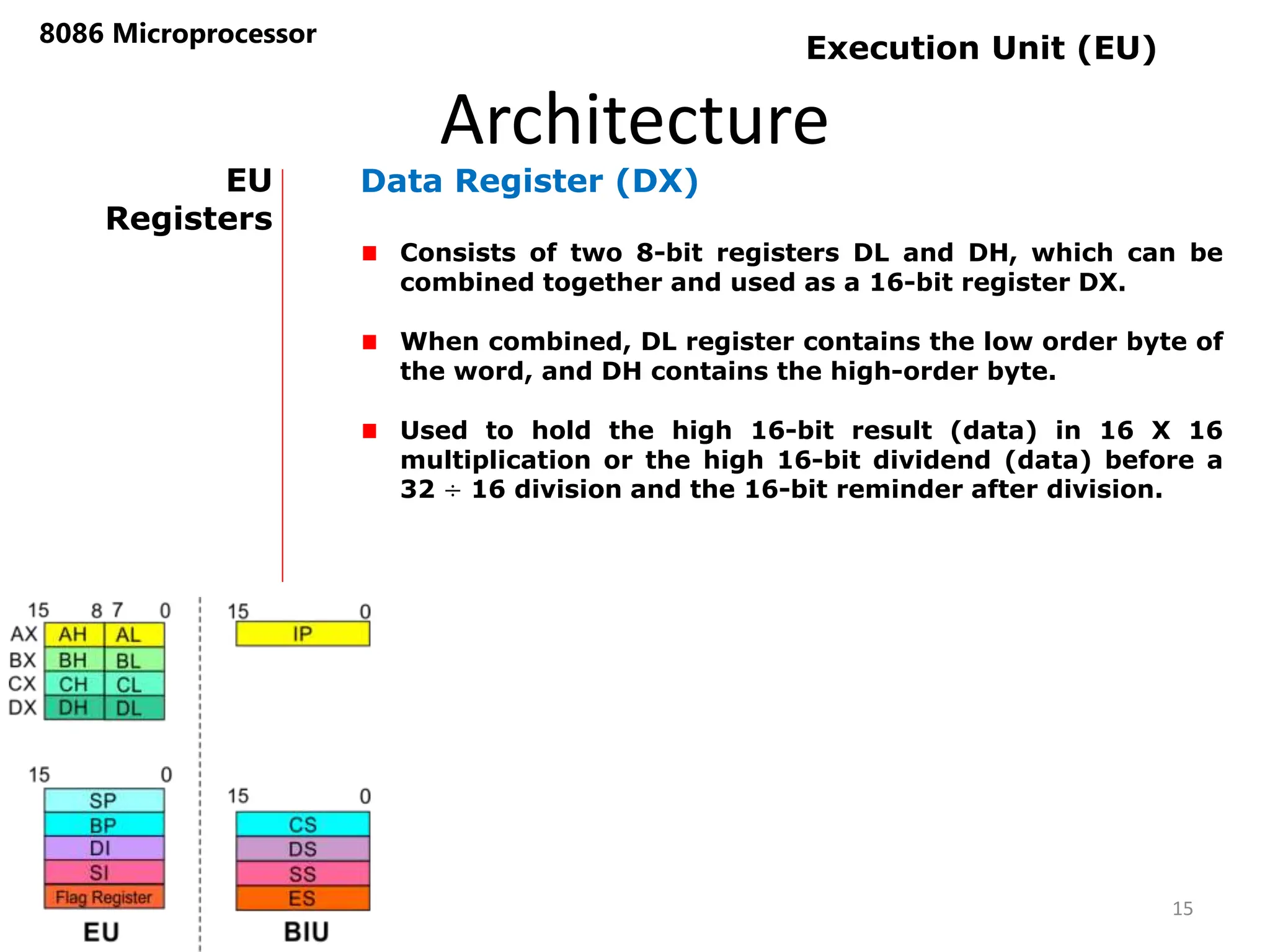
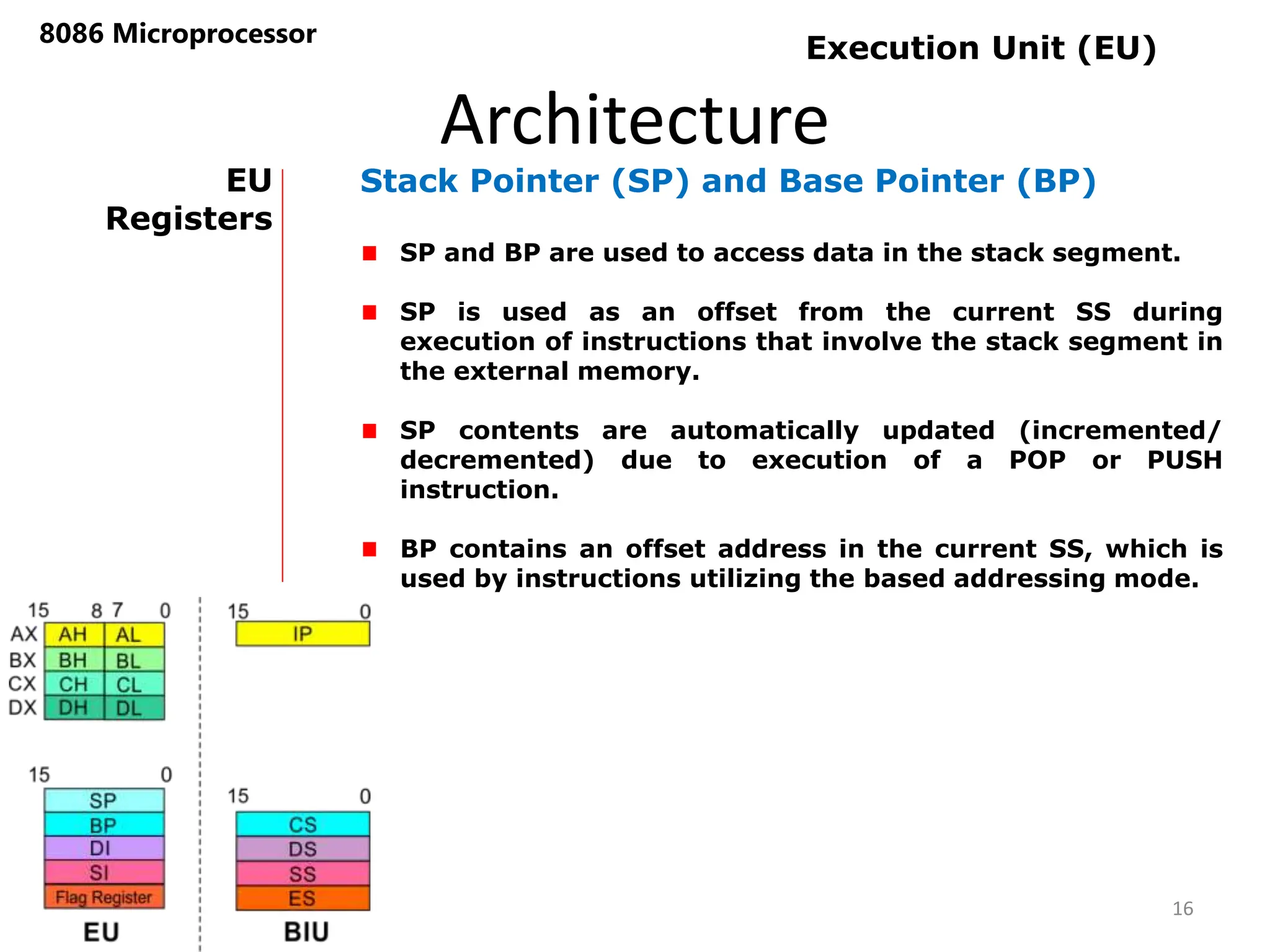
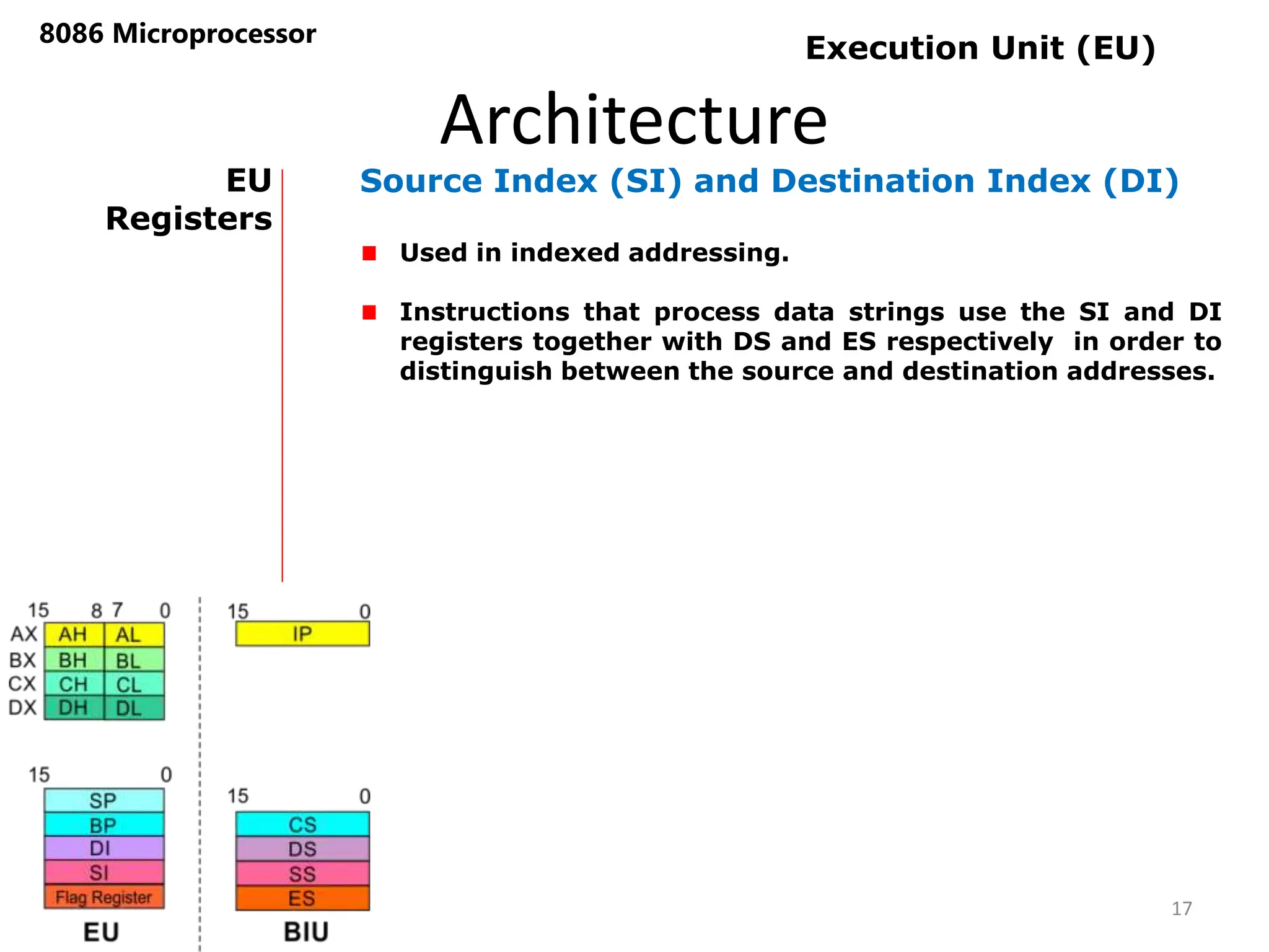
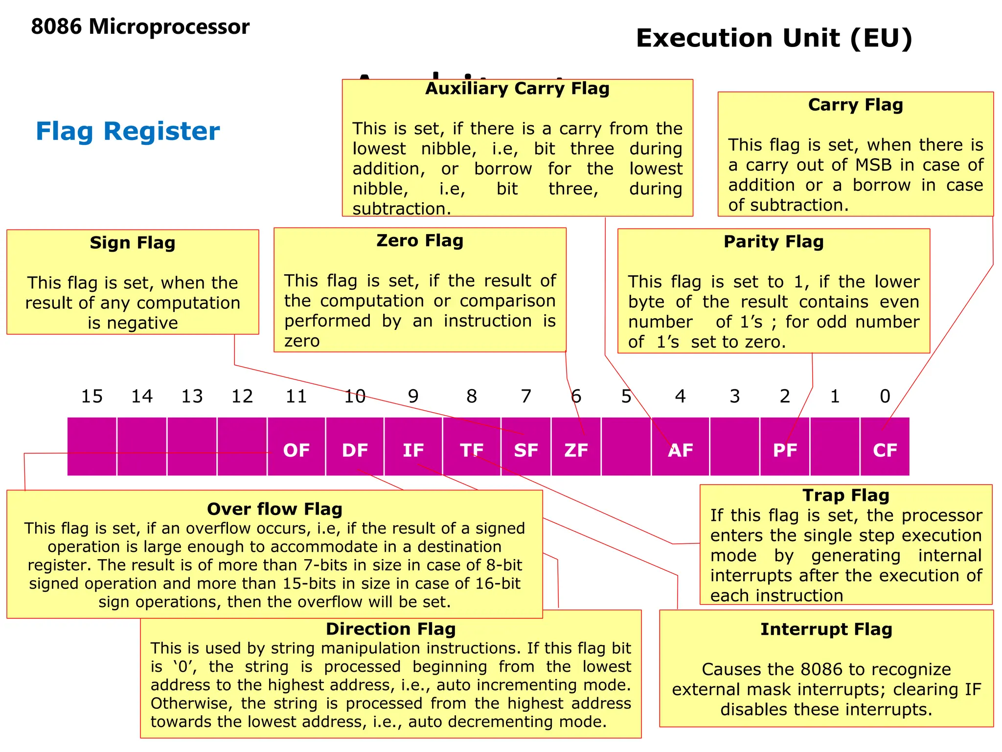
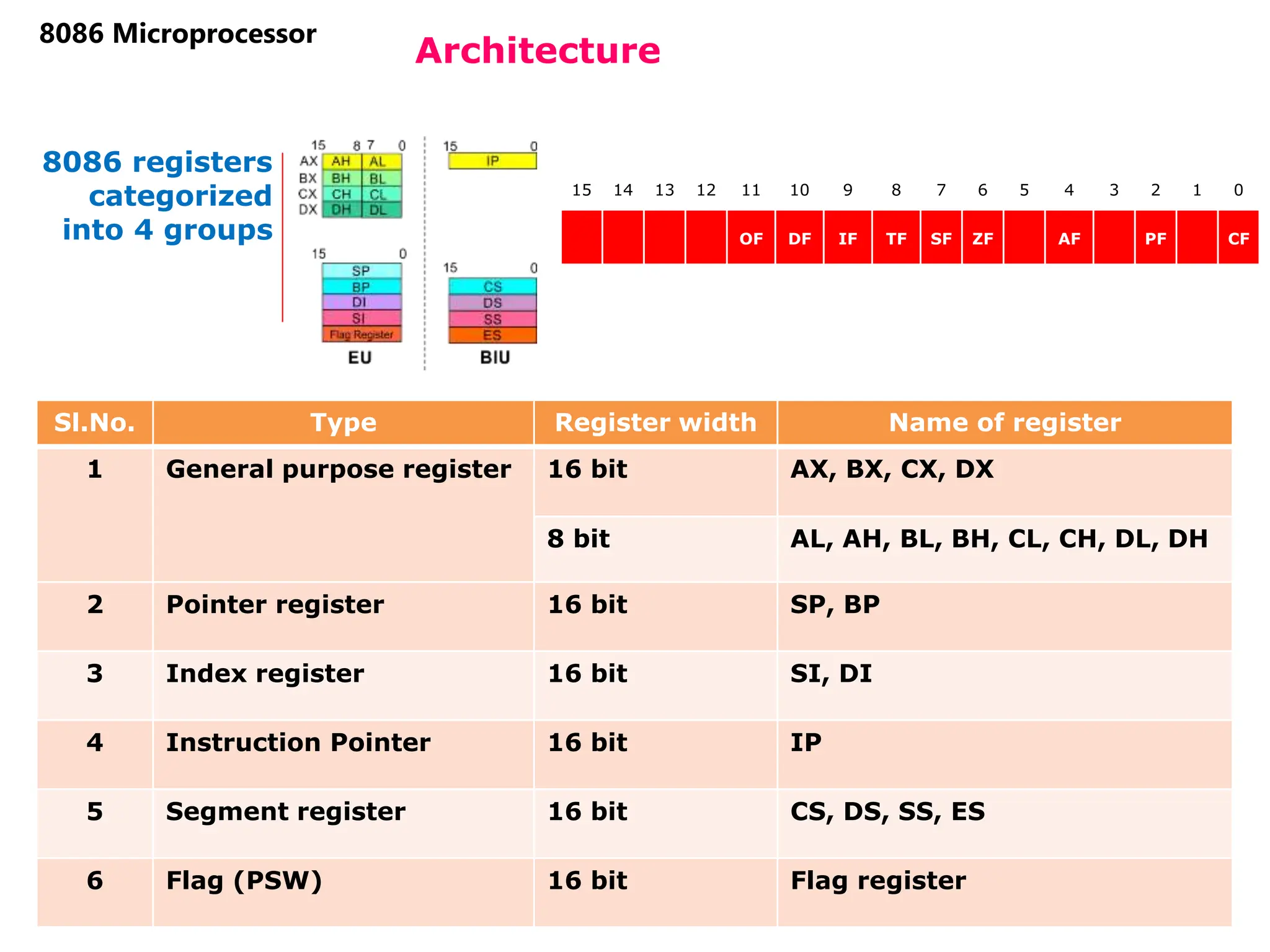
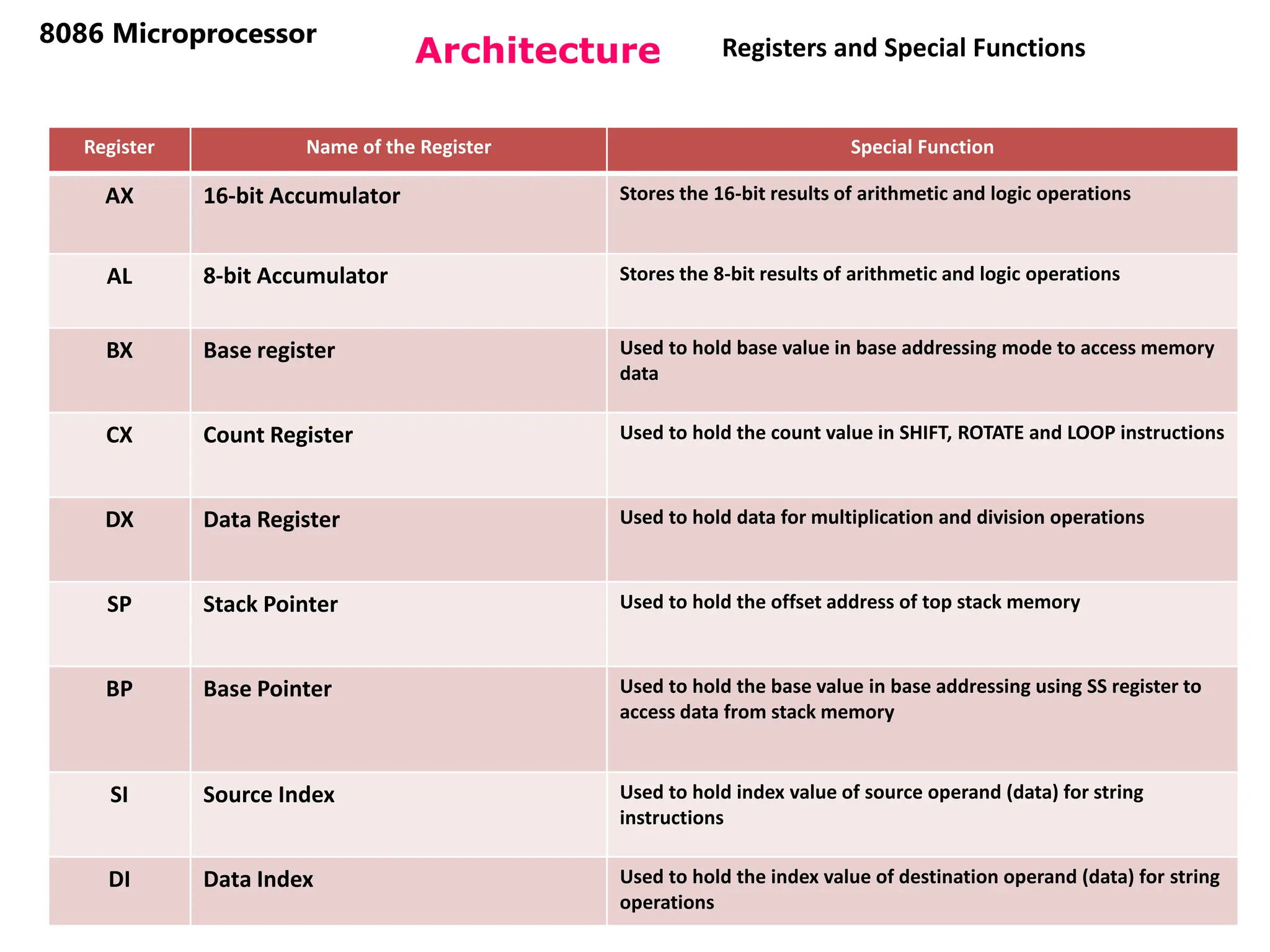
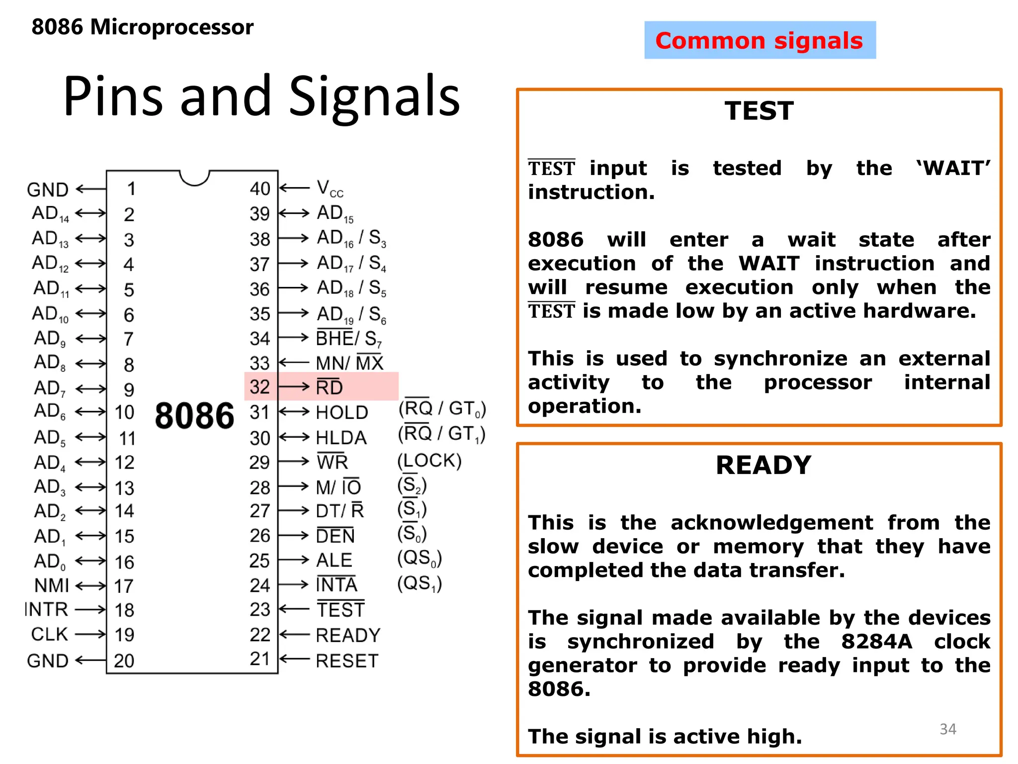
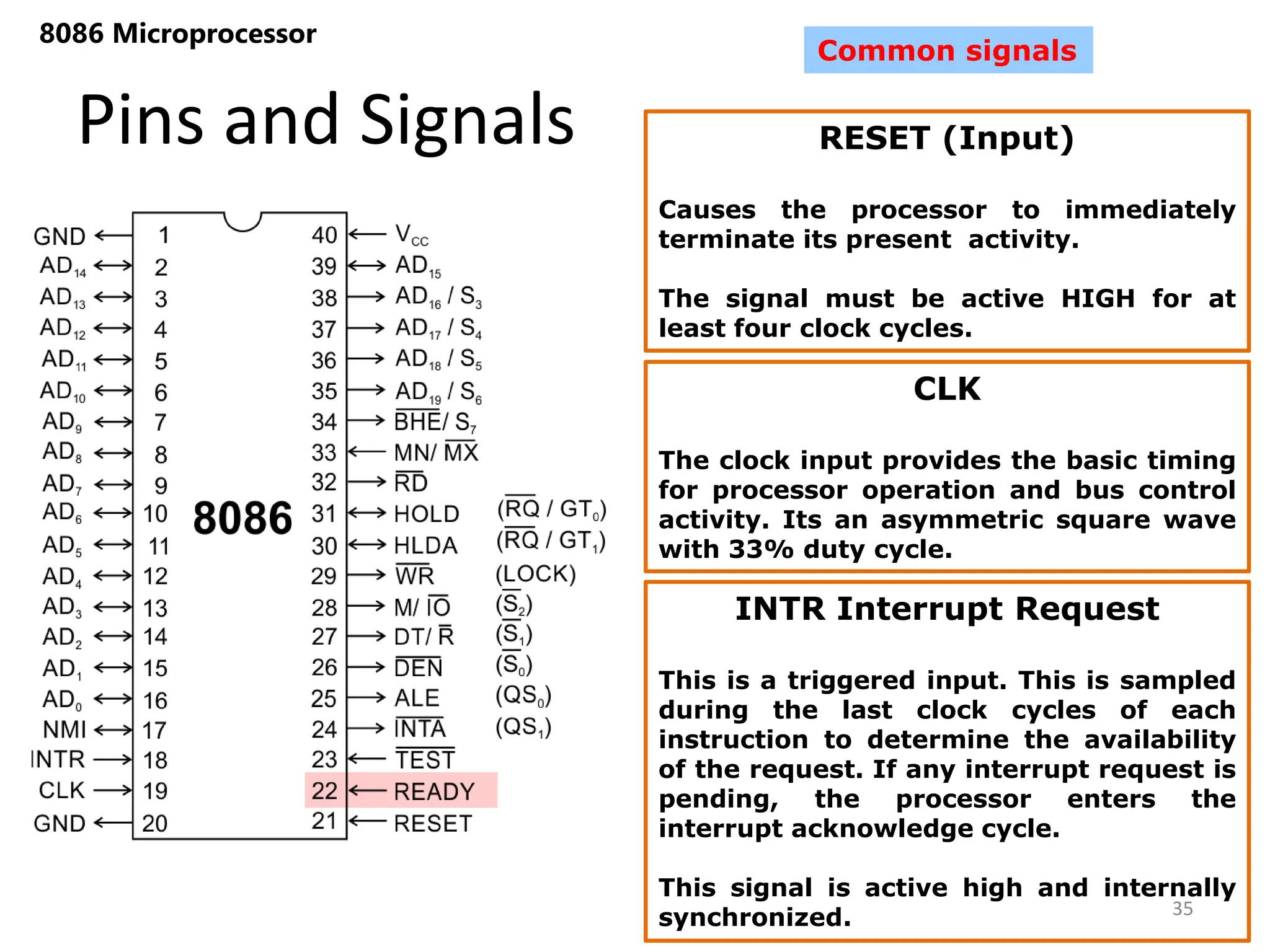
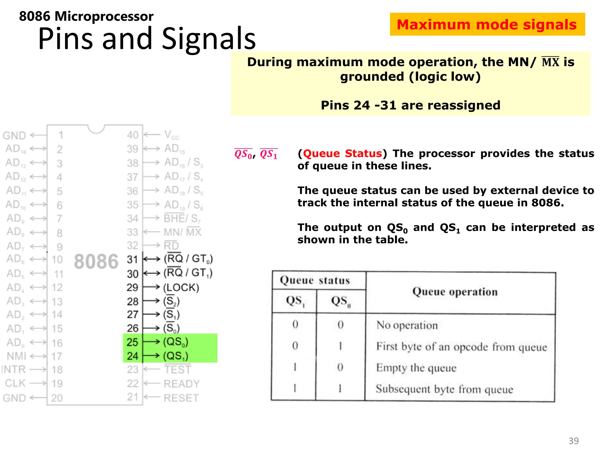
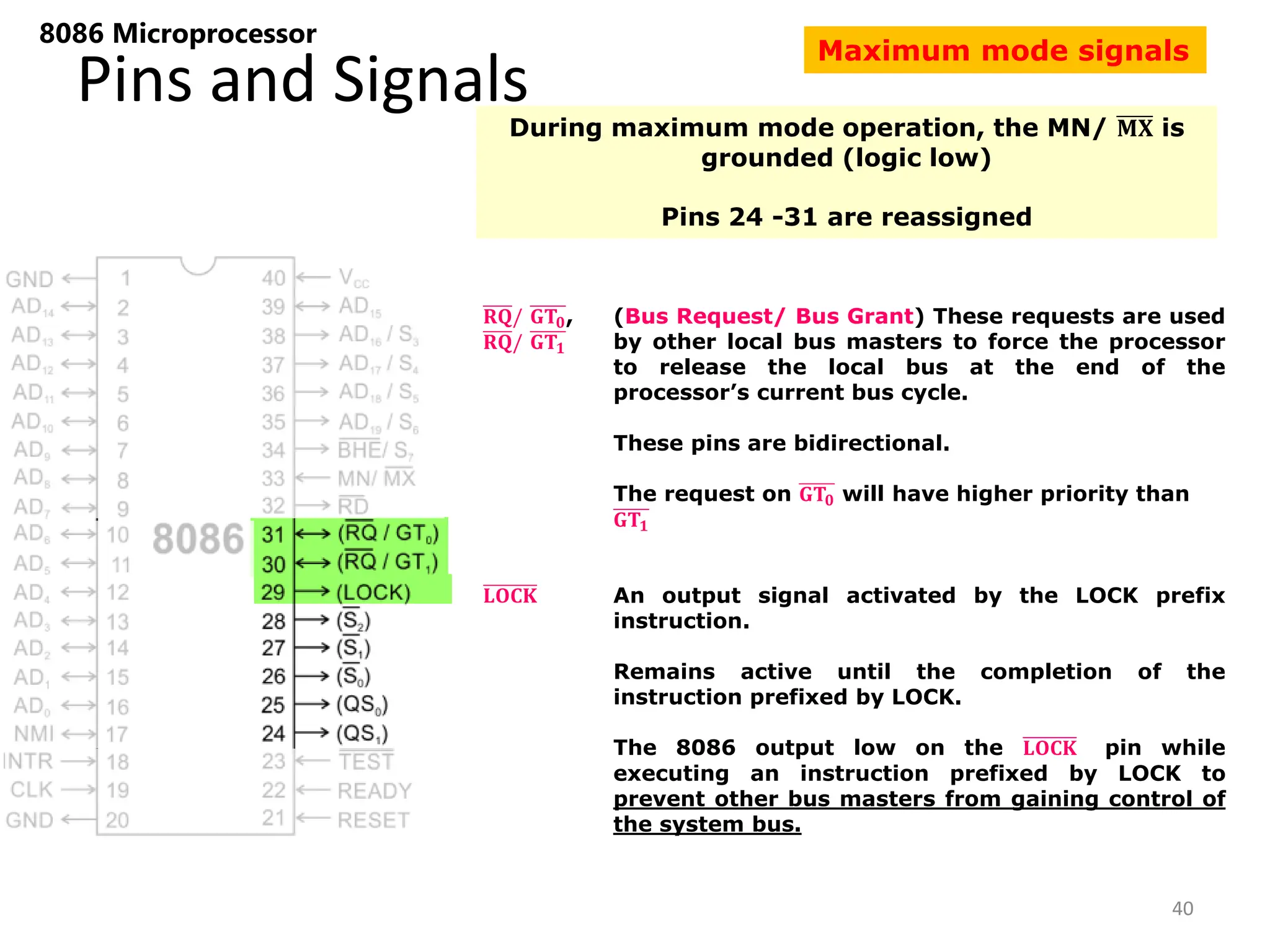
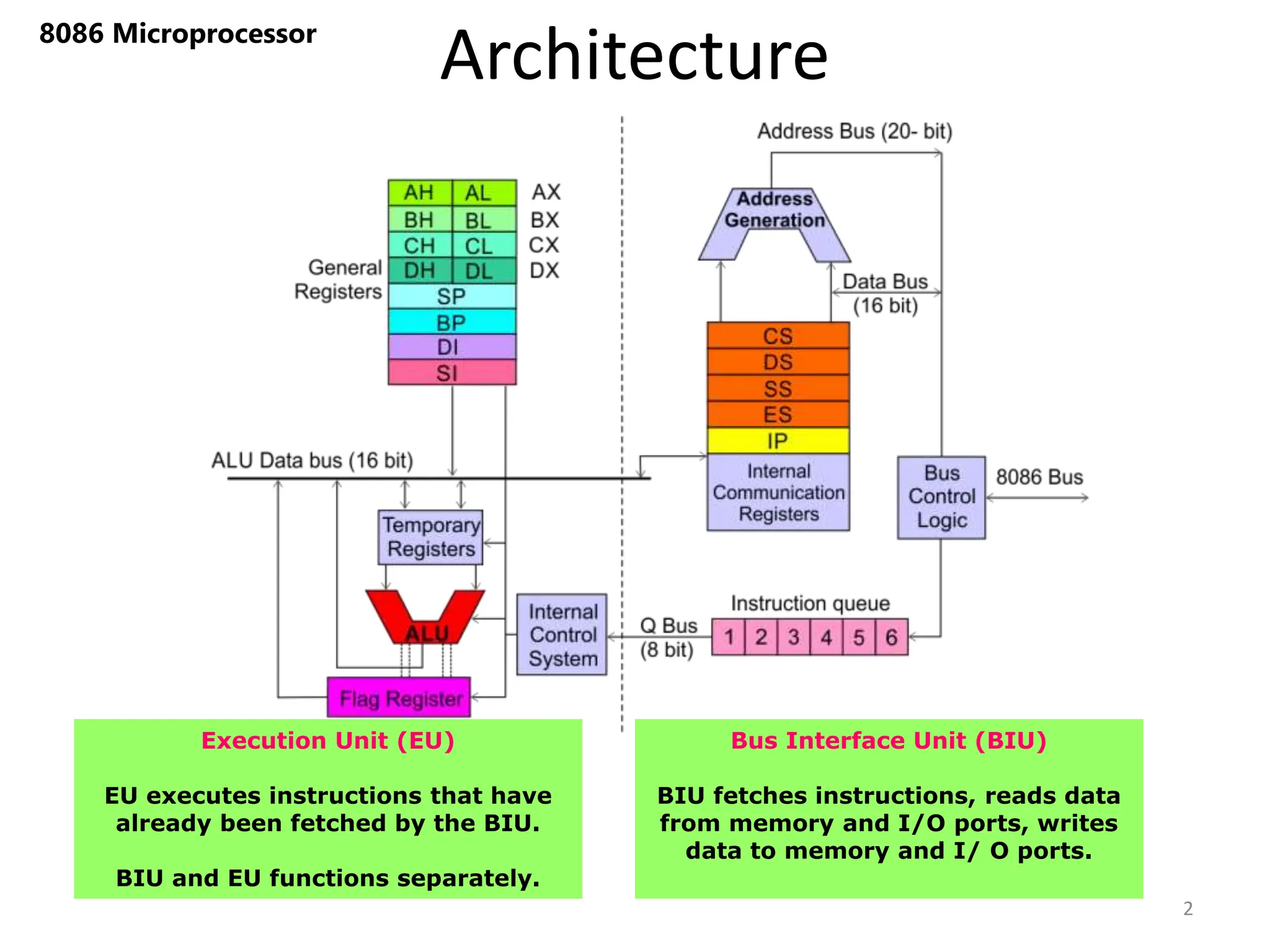
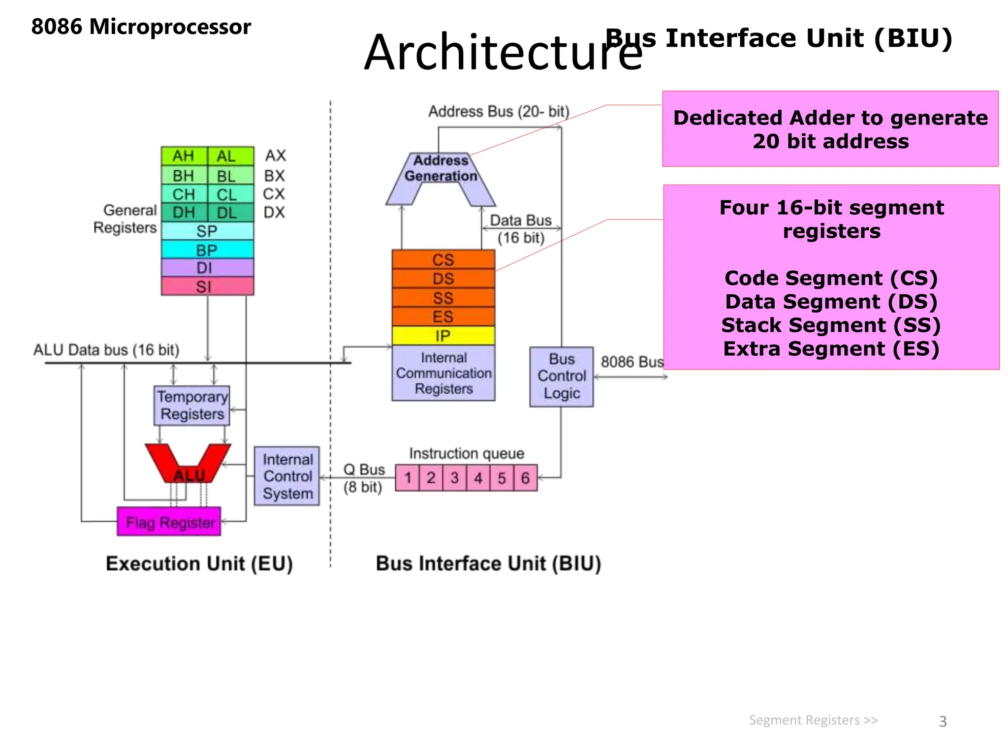
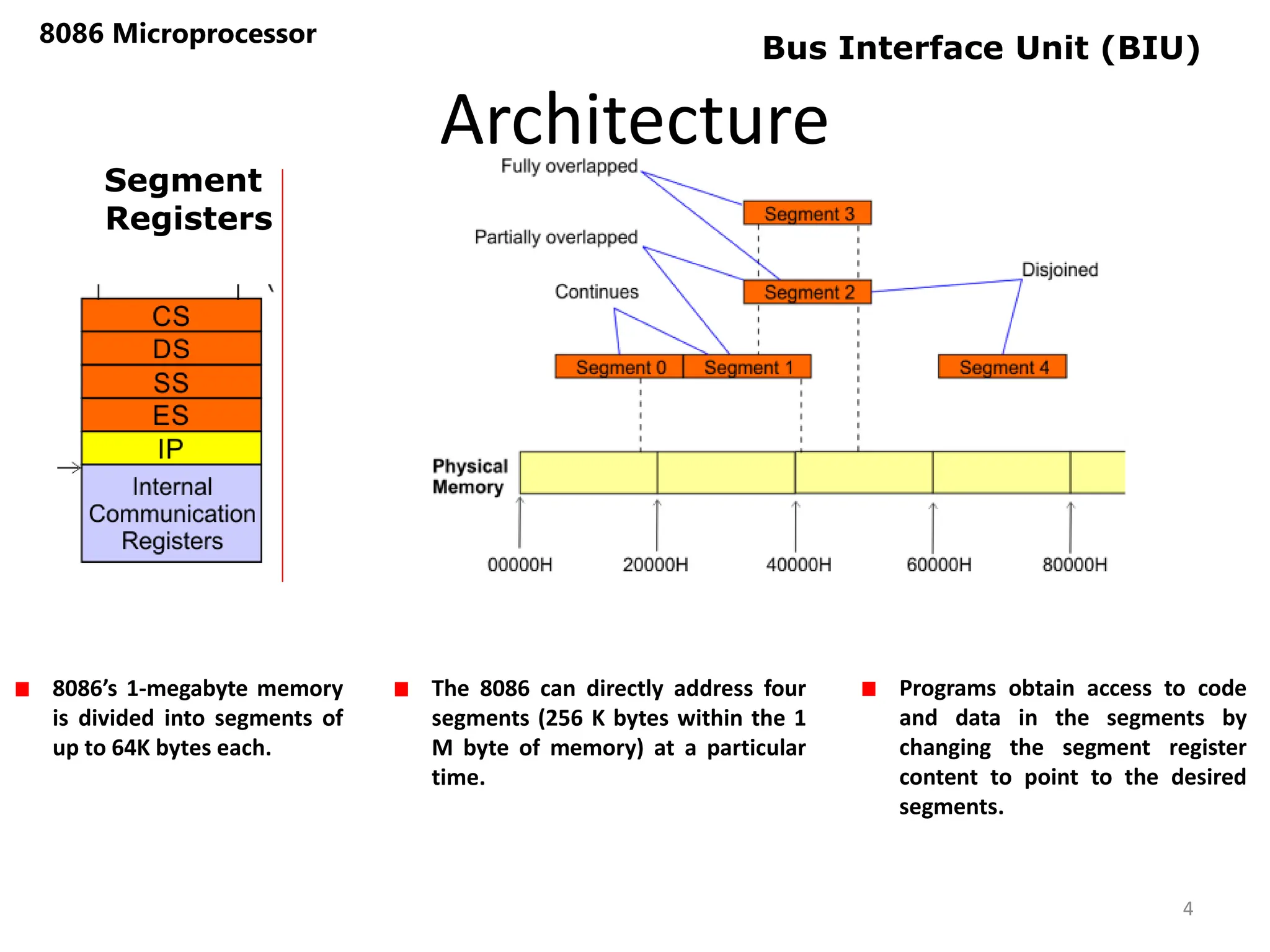
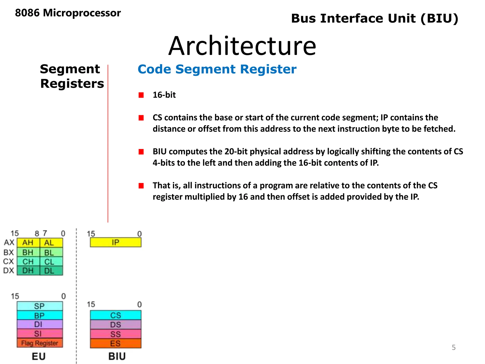
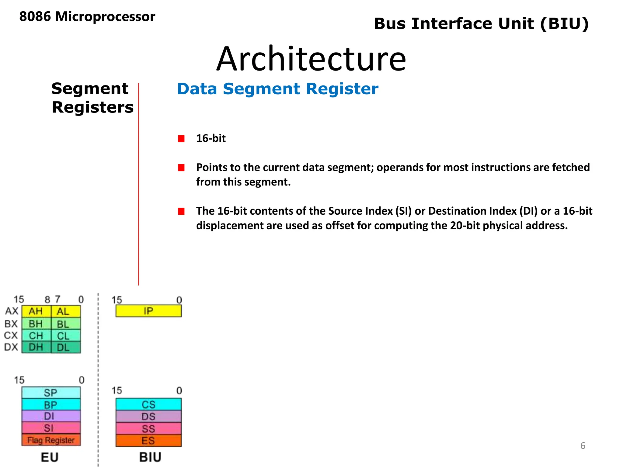
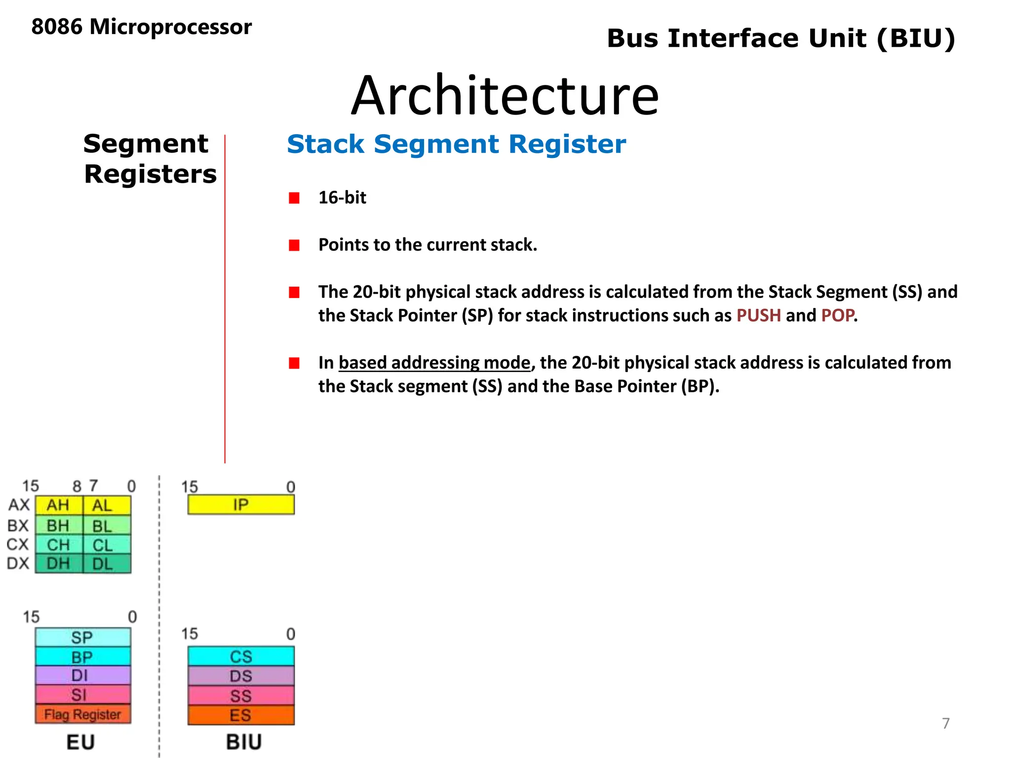
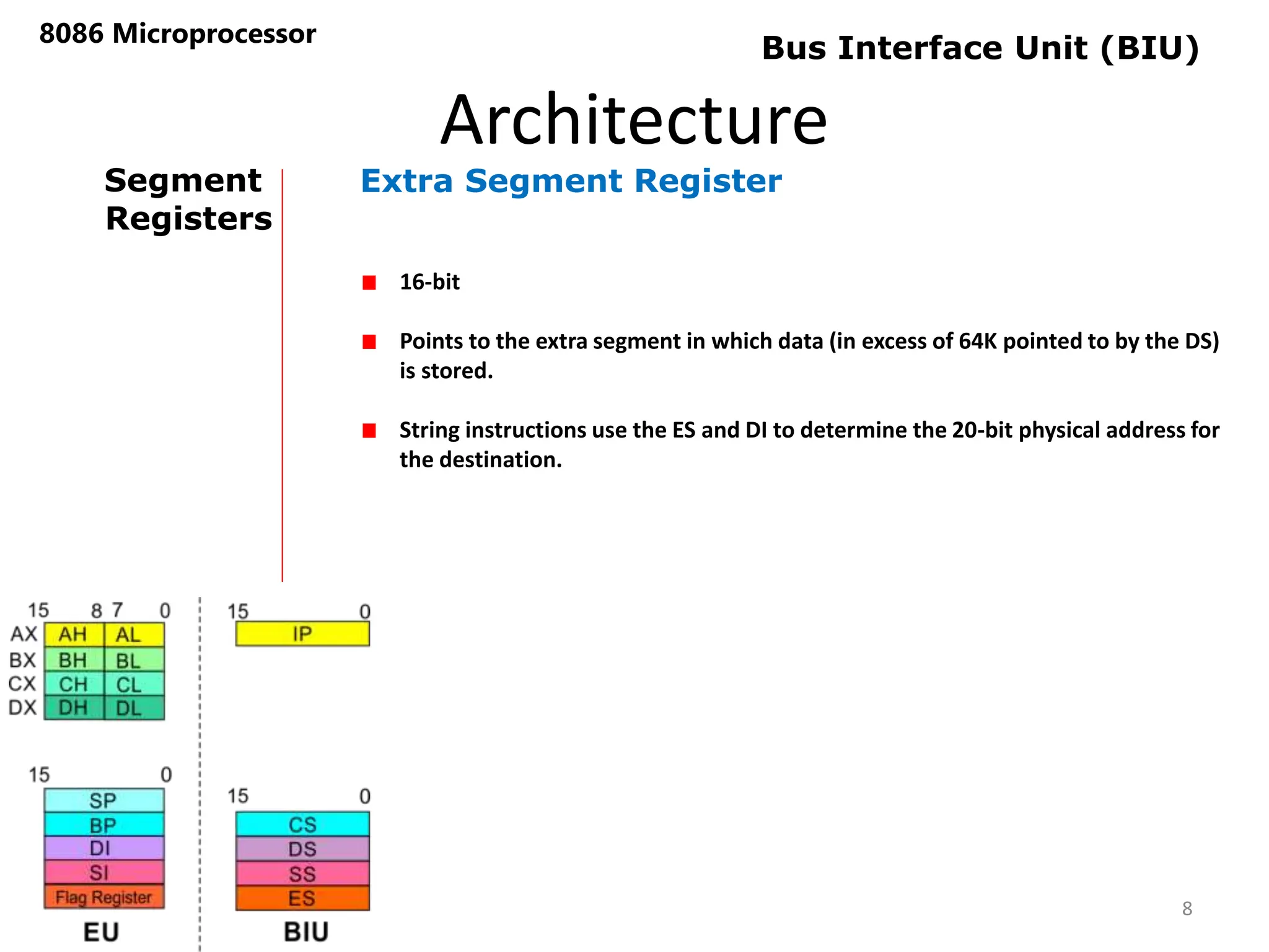
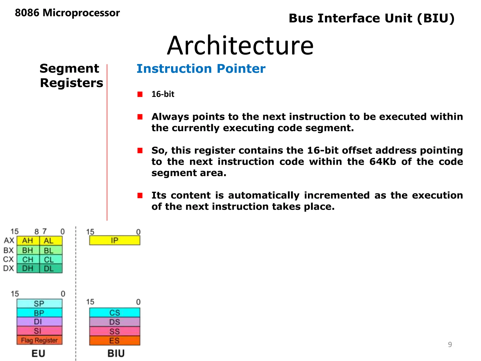
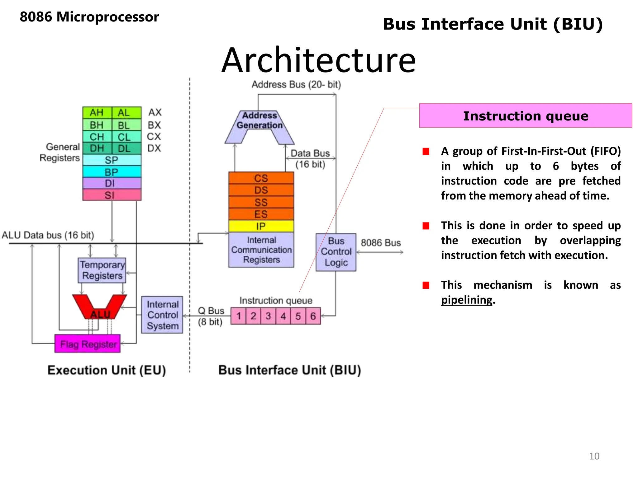
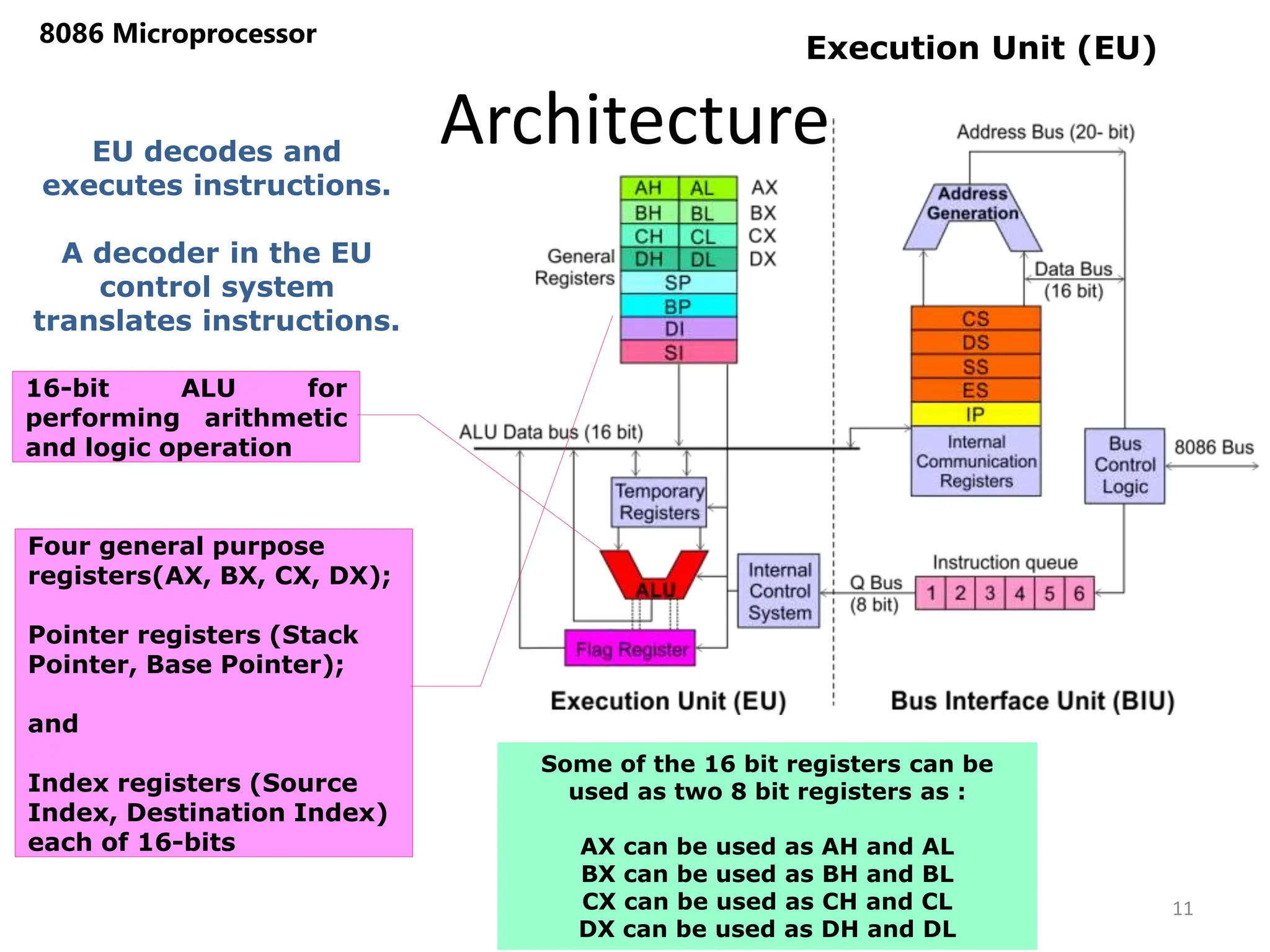
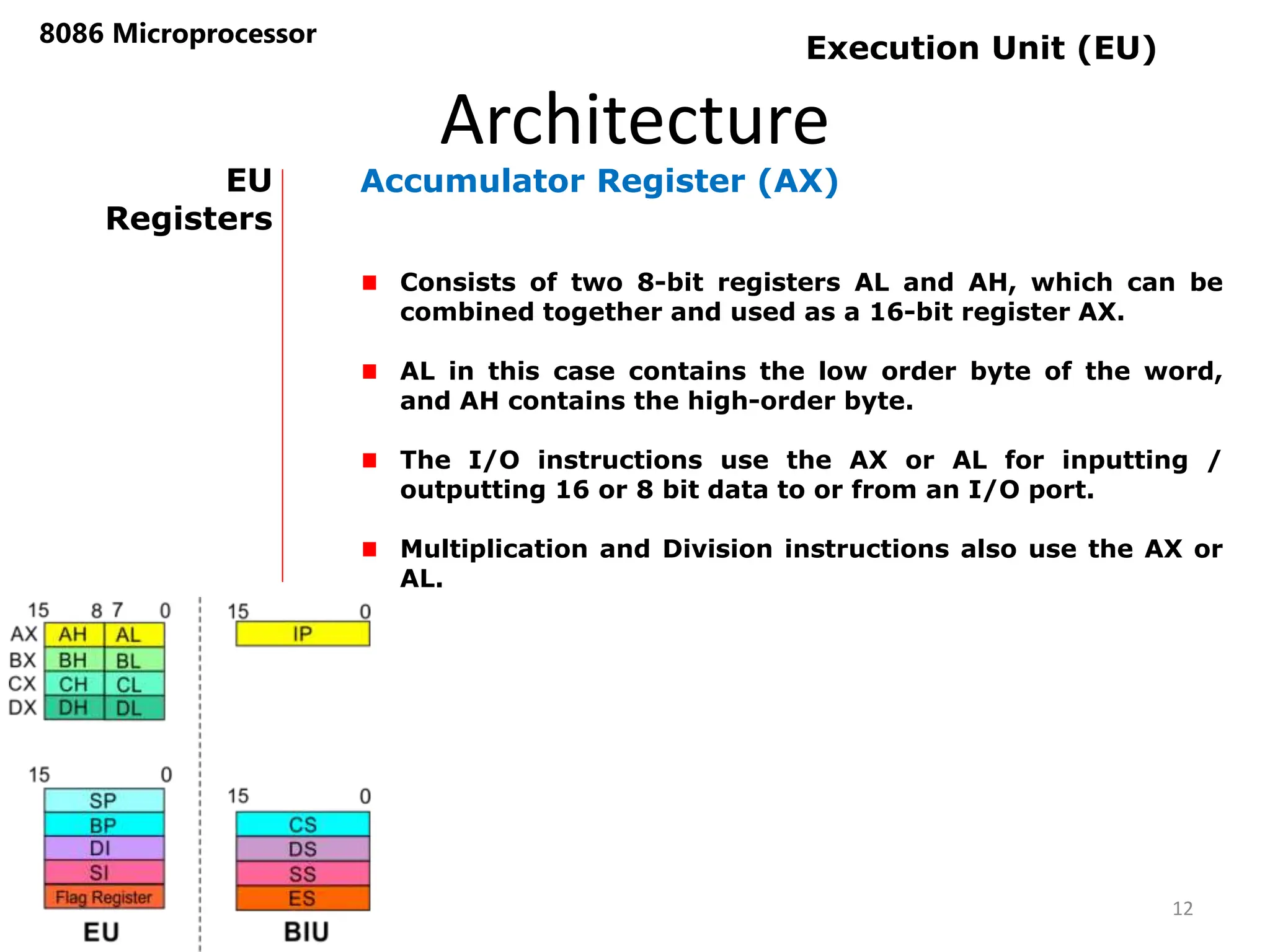
The document discusses the architecture of the 8086 microprocessor. It describes the two main components - the Execution Unit (EU) which executes instructions, and the Bus Interface Unit (BIU) which fetches instructions and reads/writes data from memory. The BIU uses segment registers to access different segments of memory. The EU contains registers like the accumulator, base, counter, and data registers. It also has flags in the flag register. Various addressing modes allow instructions to access memory using these registers.

![Architecture
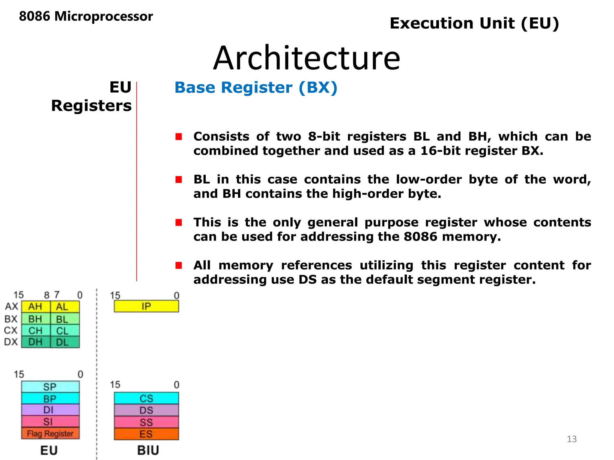
8086 Microprocessor
14
EU
Registers
Counter Register (CX)
Consists of two 8-bit registers CL and CH, which can be
combined together and used as a 16-bit register CX.
When combined, CL register contains the low order byte of
the word, and CH contains the high-order byte.
Instructions such as SHIFT, ROTATE and LOOP use the
contents of CX as a counter.
Execution Unit (EU)
Example:
The instruction LOOP START automatically decrements
CX by 1 without affecting flags and will check if [CX] =
0.
If it is zero, 8086 executes the next instruction;
otherwise the 8086 branches to the label START.](https://image.slidesharecdn.com/unitiv8086completeppt-240401054331-8c282c86/75/Unit-IV-8086-complete-ppt-architecture-and-instruction-set-pptx-14-2048.jpg)