UNIVERSITY OF SAHIWAL
Presentedto: M.Phil. Section (A+B)
2021-2023
Presented by:
Shahzad Ali Nasir (Roll no # 01)
Zeeshan Amir (Roll no # 03)
Amir Zawar (Roll no # 04)
Class: M.Phil. (A) Session: 2021-2023 Date: 17/01/2022
BASIC PRINCIPLE
This isa microscopy technique in which a beam of
electrons is transmitted through a specimen to form an
image.
The specimen is usually an ultrathin section probably
less than 100 nm thick or a thin film fabricated on
substrate.
An image is formed from the interaction of the electrons
with the sample as the beam is transmitted through the
specimen.
The image is then magnified and focused onto an
imaging device, which can be a fluorescent screen, a
layer of photographic film, or a scintillating instrument
attached to a CCD (Charge Coupled Device).
4.
WHY ELECTRONS AREUSED?
TEMs were developed because of the limited image
resolution in Visible Light Microscope (VLM), which is
imposed by the wavelength of visible light.
The resolution of a VLM is where is wavelength of
visible light and is refractive index of medium and is
semi-vertical angle of collection of lens.
The best resolution we can achieve by using 550 nm
green light is approximately 300 nm which corresponds
to 1000 atoms diameter.
Wave characteristics of matter were proposed by Louis
de Broglie in 1925 and later verified by Davisson and
Germer by electron diffraction from crystals.
5.
WHY ELECTRONS AREUSED?
It was observed that accelerating an electron at higher
potential can produce a short wavelength effect by using
the relation . This can be used to show for 100 keV
electron, associated wavelength is about 4 pm.
The best resolution obtained by TEM can be
approximated by using the relation which is far less
than resolution of VLM.
7.
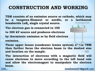
CONSTRUCTION AND WORKING
TEMconsists of an emission source or cathode, which may
be a tungsten filament or needle, or a lanthanum
hexaboride LaB6 single crystal source.
The electron gun is connected to 100
to 300 kV source and produces electrons
by thermionic emission or by field electron
emission.
These upper lenses (condenser lenses system) of the TEM
then further focus the electron beam to the desired size
and location on the sample.
The interaction of electrons with a magnetic field will
cause electrons to move according to the left hand rule
and allow the electromagnet to manipulate the electron
beam.
8.
CONSTRUCTION AND WORKING
Magneticfield allows for the formation of a magnetic
lens of variable focusing power, the lens shape
originating due to the distribution of magnetic flux.
Additionally, static electric fields can cause the
electrons to be deflected through a constant angle.
Coupling of two deflections in opposing directions with a
small intermediate gap allows for the formation of a
shift in the beam path, allowing for beam shifting in
TEM, which is important for Scanning of sample.
LIMITATIONS
There are anumber of drawbacks to the TEM technique.
Many materials require extensive sample preparation to
produce a sample thin enough to be electron transparent,
which makes TEM analysis a relatively time-consuming
process with a low throughput of samples.
The structure of the sample may also be changed during
the preparation process.
The field of view is relatively small, raising the possibility
that the region analyzed may not be characteristic of the
whole sample.
There is potential that the sample may be damaged by the
electron beam, particularly in the case of biological
materials.
Resolution limit is also an issue.
13.
INFORMATION RECEIVED FROMTEM
Transmission electron microscopy is a major analytical
method in the physical, chemical and biological
sciences.
TEMs find application in cancer research, virology and
material science as well as pollution, nanotechnology
and semiconductor research.
It provides powerful techniques for understanding
various information of materials at very high spatial
resolution, including morphology, size distribution,
crystal structure, strain, defects, chemical information
down to atomic level.
14.
TECHNIQUES USED INTEM
There are many techniques used in TEM which can give
certain information as:-
Selected-Area Electron Diffraction (SAED)
Bright Field (BF) TEM
Dark Field (DF) TEM
High-Resolution TEM (HRTEM)
High Angle Annually Dark Field STEM (HAADF-STEM)
Energy Dispersive X-ray Spectroscopy (EDS)
Electron Energy Loss Spectroscopy (EELS)
Energy Filtered TEM (EFTEM)
3D Electron Tomography
15.
TEM analysis resultsof morphology, HRTEM and
SAED of PEO (a,d), LDH (b,e) and PEO/LDH (c,f).