This document discusses timing parameters for combinational and sequential logic circuits. It defines propagation delay and contamination delay for combinational logic, and propagation delay, contamination delay, setup time, and hold time for sequential logic circuits like flip-flops. It also discusses determining maximum clock frequency for sequential circuits based on these timing parameters, modeling delays from gates and interconnect, using clock trees, and issues related to clock skew and jitter.
Digital timer switches are utilized to control the task of electrical gadgets dependent on a customized timetable. This undertaking portrays a programmable digital timer dependent on the PIC16F628A microcontroller that can be customized to plan the on and off activity of an electrical apparatus. The apparatus is controlled through a hand-off switch. This clock change enables you to set both on and off time. That implies, you can program when would you like to turn the gadget on and for to what extent you need it to be stayed on. The greatest time interim that you can set for on and off activity is 99 hours and 59 minutes. The task gives an intuitive UI utilizing a 16×2 character LCD alongside 4 push catches.
- Designed a standard cells with gates including Inverter, two input NAND, two Input NOR, two Input XOR, 2:1 Multiplexer, AOI22, OAI3222 and D Flip Flop with minimum area & diffusion breaks by using IBM130 nm process technology.
- Involved library characterization using NCX, RTL synthesis of VHDL code of 32 bit ALU Chip design using Synopsys Design Vision.
FYBSC IT Digital Electronics Unit IV Chapter II Sequential Circuits- Flip-FlopsArti Parab Academics
Sequential Circuits: Flip-Flop:
Introduction, Terminologies used, S-R flip-flop, D flip-fop, JK flipflop, Race-around condition, Master – slave JK flip-flop, T flip-flop, conversion from one type of flip-flop to another, Application of flipflops.
V/F control of Induction Motor - Variable voltage and Variable frequencyCitharthan Durairaj
This presentation describes Principle of Variable voltage and Variable frequency- the open loop & closed loop Voltage/Frequency (V/F) control of Induction motor with torque speed characteristics -
This presentation describes the
Line Voltage Control - Torque Speed Characteristics - Methods -Advantages - Disadvantages - Applications of Voltage control
Traffic sign board ad spots in Anna Nagar by Brand On Anything
Contact Person for Traffic Sign Board Ads
Mr. Ilias
Number : +91-99405-53791 / 044-4333 5426 (call for immediate booking)
Email : brand@brandonanything.com
Website : www.brandonanything.com
Check our latest works here
Blog : http://brandonanything.blogspot.in
Thanks for giving us the opportunity to know about our services.
We are a young, dynamic and creative branding agency who take care of all the branding activities starting from printing both offset and flex, supplying promotion materials like standees, promotion tables, umbrellas, tshirts, badges ..etc and instore (visual merchandising) & office branding with sun boards, vinyl ..etc.
We have attached our catalogue for your reference. Awaiting to hear from you at the earliest.
Speak to our branding co-ordinator for all your branding solutions.
Nasar (+91-72006 43774)
Branding Co-Ordinator
Brand on Anything
#151, 8th Street, Secretariate Colony,
Kellys, Chennai-10
Brandline : 044-43335426
Web : brandonanything.com
The paper describes the basic of Timing analysis like setup time, hold time, delays in logic circuits, timing violations and different types of timing paths like flip-flop to flip-flop path, clock gating path, asynchronous signal path, half cycle path, flip-flop to output path, input to flip-flop path and input to output path.
DESIGN AND PERFORMANCE ANALYSIS OF NINE STAGES CMOS BASED RING OSCILLATORVLSICS Design
This paper deals with the design and performance analysis of a ring oscillator using CMOS 45nm technology process in Cadence virtuoso environment. The design of optimal Analog and Mixed Signal (AMS) very large scale integrated circuits (VLSI) is a challenging task for the integrated circuit(IC) designer. A Ring Oscillator is an active device which is made up of odd number of NOT gates and whose output oscillates between two voltage levels representing high and low. There are a number of challenges ahead while designing the CMOS Ring Oscillator which are delay, noise and glitches. CMOS is the technology of choice for many applications, CMOS oscillators with low power, phase noise and timing jitter are highly desired. In this paper, we have designed a CMOS ring oscillator with nine stages.Previously, the researchers were unable to reduce the phase noise in ring oscillators substantially with nine stages. We have successfully reduced the phase noise to -6.4kdBc/Hz at 2GHz center frequency of oscillation.
SCAN CHAINS TESTING FOR LATCHES TO REDUCE AREA AND THE POWER CONSUMPTIONcscpconf
During the test mode of flip flop in a chip, a set of input vectors are sent through the flip-flop, it
consumes more power consumption than in the normal functional mode. In this paper, we
propose a latch with bi -stable element which reduces area as well as the power consumed. The
latch proposed consists of simple basic gates involving two inverters back to back which acts as
a bi-stable element and a transmission gate with the clock signal used to enable and disable the
rest of the circuit with impact on running the latch on Static Timing Analysis. The input test
vectors are either given by Automatic Test Pattern Generation (ATPG) or many other methods.
We model this using T-Simulation Program with Integrated Circuit Emphasis (T-SPICE) and see the power consumed.
Clock Generator/Jitter Cleaner with Integrated VCOsPremier Farnell
This training module provide a basic understanding of how clocks work and the various functions & key parameters of clocks, and introduces the CDCE62005 clock generator
Institute of infrastructure technology research and management (IITRAM) Ahmedabad. This is the project report given to us in the control sytem lab. This is basically a Servo postion control. Here we are using PID controller.
Operation “Blue Star” is the only event in the history of Independent India where the state went into war with its own people. Even after about 40 years it is not clear if it was culmination of states anger over people of the region, a political game of power or start of dictatorial chapter in the democratic setup.
The people of Punjab felt alienated from main stream due to denial of their just demands during a long democratic struggle since independence. As it happen all over the word, it led to militant struggle with great loss of lives of military, police and civilian personnel. Killing of Indira Gandhi and massacre of innocent Sikhs in Delhi and other India cities was also associated with this movement.
Welcome to TechSoup New Member Orientation and Q&A (May 2024).pdfTechSoup
In this webinar you will learn how your organization can access TechSoup's wide variety of product discount and donation programs. From hardware to software, we'll give you a tour of the tools available to help your nonprofit with productivity, collaboration, financial management, donor tracking, security, and more.
Synthetic Fiber Construction in lab .pptxPavel ( NSTU)
Synthetic fiber production is a fascinating and complex field that blends chemistry, engineering, and environmental science. By understanding these aspects, students can gain a comprehensive view of synthetic fiber production, its impact on society and the environment, and the potential for future innovations. Synthetic fibers play a crucial role in modern society, impacting various aspects of daily life, industry, and the environment. ynthetic fibers are integral to modern life, offering a range of benefits from cost-effectiveness and versatility to innovative applications and performance characteristics. While they pose environmental challenges, ongoing research and development aim to create more sustainable and eco-friendly alternatives. Understanding the importance of synthetic fibers helps in appreciating their role in the economy, industry, and daily life, while also emphasizing the need for sustainable practices and innovation.
The French Revolution, which began in 1789, was a period of radical social and political upheaval in France. It marked the decline of absolute monarchies, the rise of secular and democratic republics, and the eventual rise of Napoleon Bonaparte. This revolutionary period is crucial in understanding the transition from feudalism to modernity in Europe.
For more information, visit-www.vavaclasses.com
Read| The latest issue of The Challenger is here! We are thrilled to announce that our school paper has qualified for the NATIONAL SCHOOLS PRESS CONFERENCE (NSPC) 2024. Thank you for your unwavering support and trust. Dive into the stories that made us stand out!
Acetabularia Information For Class 9 .docxvaibhavrinwa19
Acetabularia acetabulum is a single-celled green alga that in its vegetative state is morphologically differentiated into a basal rhizoid and an axially elongated stalk, which bears whorls of branching hairs. The single diploid nucleus resides in the rhizoid.
Biological screening of herbal drugs: Introduction and Need for
Phyto-Pharmacological Screening, New Strategies for evaluating
Natural Products, In vitro evaluation techniques for Antioxidants, Antimicrobial and Anticancer drugs. In vivo evaluation techniques
for Anti-inflammatory, Antiulcer, Anticancer, Wound healing, Antidiabetic, Hepatoprotective, Cardio protective, Diuretics and
Antifertility, Toxicity studies as per OECD guidelines
Honest Reviews of Tim Han LMA Course Program.pptxtimhan337
Personal development courses are widely available today, with each one promising life-changing outcomes. Tim Han’s Life Mastery Achievers (LMA) Course has drawn a lot of interest. In addition to offering my frank assessment of Success Insider’s LMA Course, this piece examines the course’s effects via a variety of Tim Han LMA course reviews and Success Insider comments.
Safalta Digital marketing institute in Noida, provide complete applications that encompass a huge range of virtual advertising and marketing additives, which includes search engine optimization, virtual communication advertising, pay-per-click on marketing, content material advertising, internet analytics, and greater. These university courses are designed for students who possess a comprehensive understanding of virtual marketing strategies and attributes.Safalta Digital Marketing Institute in Noida is a first choice for young individuals or students who are looking to start their careers in the field of digital advertising. The institute gives specialized courses designed and certification.
for beginners, providing thorough training in areas such as SEO, digital communication marketing, and PPC training in Noida. After finishing the program, students receive the certifications recognised by top different universitie, setting a strong foundation for a successful career in digital marketing.
Digital Artifact 2 - Investigating Pavilion Designs
Timing notes 2006
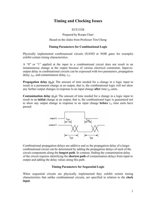
1. 1
Timing and Clocking Issues
ECE152B
Prepared by Roopa Chari
Based on the slides from Professor Tim Cheng
Timing Parameters for Combinational Logic
Physically implemented combinational circuits (NAND or NOR gates for example)
exhibit certain timing characteristics.
A “0” or “1” applied at the input to a combinational circuit does not result in an
instantaneous change at the output because of various electrical constraints. Input-to-
output delay in combinational circuits can be expressed with two parameters, propagation
delay, tpd, and contamination delay, tcd.
Propagation delay (tpd): The amount of time needed for a change in a logic input to
result in a permanent change at an output, that is, the combinational logic will not show
any further output changes in response to an input change after time tpd units.
Contamination delay (tcd): The amount of time needed for a change in a logic input to
result in an initial change at an output, that is, the combinational logic is guaranteed not
to show any output change in response to an input change before tcd time units have
passed.
Combinational propagation delays are additive and so the propagation delay of a larger
combinational circuit can be determined by adding the propagation delays of each of the
circuit components along the longest path. In contrast, finding the contamination delay
of the circuit requires identifying the shortest path of contamination delays from input to
output and adding the delay values along this path.
Timing Parameters for Sequential Logic
When sequential circuits are physically implemented they exhibit certain timing
characteristics that unlike combinational circuits, are specified in relation to the clock
input.
2. 2
Latch vs. Flip-Flop
A latch is level-sensitive while a flip-flop is edge triggered. A latch stores when the clock
level is low and is transparent when the level is high. A flip-flop stores when the clock
rises and is mostly never transparent. Since flip-flops only change value in response to a
change in the clock value, timing parameters can be specified in relation to the rising (for
positive edge-triggered) or falling (for negative-edge triggered) clock edge.
The following parameters specify sequential circuit behavior. Note that these are all for
positive edge-triggered flip-flops unless otherwise specified, but are easily applied to
negative edge triggered flip-flops as well.
Propagation delay (tclk−q): The amount of time needed for a change in the flip-flop clock
input D to result in a change at the flip-flop output Q. When the clock edge arrives, the D
input value is transferred to output Q. After time tclk−q the output is guaranteed not to
change value again until another clock edge trigger arrives.
Contamination delay (tcd): This value indicates the amount of time needed for a change
in the flip-flop clock input to result in the initial change at the flip-flop output Q. The
output of the flip-flop maintains its initial value until time tcd has passed and is
guaranteed not to show any output change in response to an input change until after tcd
has passed.
Note: delays can be different for both rising and falling transitions.
Setup time (tsu): The amount of time before the clock edge that data input D must be
stable the rising clock edge arrives.
Hold time (thold): This indicates the amount of time after the clock edge arrives that data
input D must be held stable in order for the flip-flop to latch the correct value. Hold time
is always measured from the rising clock edge (for positive edge-triggered) to a point
after the clock edge.
3. 3
Setup and hold times are restrictions that a flip-flop places on combinational or
sequential circuitry that drives a flip-flop D input. The circuit has to be designed so the D
input signal arrives at least tsu time units before the clock edge and does not change until
at least thold time units after the clock edge. If either of these restrictions is violated for
any of the flip-flops in the circuit, the circuit will not operate correctly. These restrictions
limit the maximum clock frequency at which the circuit can operate.
Determining the Maximum Clock Frequency for a Sequential Circuit
Most digital circuits contain both combinational components (gates, muxes, adders, etc.)
and sequential components (flip-flops). These components can be combined to form
sequential circuits that perform computation and store results. By using combinational
and sequential component parameters, it is possible to determine the maximum clock
frequency at which a circuit will operate and generate correct results. This analysis can
best be examined through use of an example.
Example 1: For the circuit shown below, assume the delay through the register (tclk-q) is
0.6ns and the delay through each logic block is indicated inside the box. Assume that the
positive edge-triggered registers have a set-up time tsu of 0.4ns. What is the minimum
clock period?
The first step is model the given circuit so that the datapath between flip-flops are characterized
by the longest and shortest combinational delays between the flip-flops.
direction of clock
4. 4
Let Tclk be the clock period. Then,
Tclk ≥ tclk-q (register) + tpd logic (longest) + tsu (destination register)
Tclk ≥ 0.6 ns + 8 ns + 0.4 ns
Tclk ≥ 9 ns
Delay Modeling
Gate propagation delay (tPHL and tPLH): Gate propagation delay is measured from 50%
input to 50% of the output. tPHL is measured from 50% of the rising edge of the input
voltage to 50% of the rising edge of the output voltage. Similarly, tPLH is measured from
50% of the falling edge of the input voltage to 50% of the falling edge of the output
voltage.
Interconnect Delay: This is delay caused by wires. Interconnect introduces three types
of parasitic effects – capacitive, resistive, and inductive – all of which influence signal
integrity and degrade the performance of the circuit. After the signal frequencies of our
interests (up to several GHz), we can ignore the effects of inductance of interconnect.
When gate G1 drives gate G2, we can model the circuit as the one showing below in the
right-hand side figure where Rout is the output resistance of G1, Rin and Cin are the
interconnect resistance and capacitance, and CL is the input capacitance of G2.
This model can be further
simplified as the one shown in the
right. Now if Vin (i.e. output of G1)
switches from 0V to VDD, the
waveform at Vout (i.e. input of G2)
can be expressed as:
Vout = VDD (1- e-t/RC
)
Vin Vout
(output
of G1)
(input
of G2)R= Rout+Rint
C=Cin+CL
5. 5
Definition: Rise time (Fall time) - The time it takes for a waveform to rise from 10% to
90% (90% to 10%) of its steady state value – as illustrated below.
The time for the waveform Vout = VDD (1- e-t/RC
) to rise from 0.1VDD from 0.9VDD can be
easily calculated:
Note that the rise time is linearly proportional to the product of (Rout+Rin) and (Cin+CL).
So, if the interconnect is long, Rin and Cin will be large, and, in turn, the rise time will be
long. Similarly, if a gate drives a large number of gates, the rise time will be long too as
CL, which is proportional to the number of driven gates, is large.
Clock Trees
If the number of flip-flops driven by the clock line is large, the clock rise time (also
called slew rate) will be unacceptably long. The solution to this problem is to use a clock
power up tree which means adding buffers into the clock tree.
When designing a clock distribution network, the absolute delay from a central clock
source to the clock elements is irrelevant, only the relative phase between two clock
elements is important.
When designing clock trees in this way, first determine the number of levels your clock
tree can have. This will depend on the total number of flip-flops in the circuit and the
number of fan outs (to flip-flops or buffers) that you are limited to. See the examples in
the lecture slides.
VOL
VOH
Rise time
VOL
VOH
Fall time
90%
10%
90%
10%
Rise Time ~= 2.2 * R * C
6. 6
Clock Skew and Clock Jitter
Clock Skew (δ): The spatial variation in arrival time of a clock transition is known as
clock skew. The clock skew between two points j and k is given by tj – tk, where tj – tk are
the rising edge of the clock with respect to the reference. Clock skew is constant from
cycle to cycle and does not cause clock period variation, but only phase shift.
Clock skew might cause the race problem – illustrated in the lecture slides.
Clock Jitter: Clock jitter refers to the temporal variation of the clock period, that is, the
clock period can expand or reduce on a cycle-by-cycle basis.
Variation of the pulse width is important for level sensitive clocking.
Positive and Negative Clock Skew
Positive Skew: Clock and data flow in the same direction.
Minimum cycle time: Tclk + δ ≥ tclk-q + CriticalPathDelay+ tsu
7. 7
This means that clock skew has the potential to improve the performance of the circuit
(minimum required clock period reduces!). However, increasing clock skew makes the
circuit more susceptible to race conditions.
Negative Skew: Clock and data flow in opposite directions
Note: Receiving edge arrives before the launching edge
On one hand, negative skew adversely impacts the performance (increase the clock
period). On the other hand, negative skew implies that the system never has the race
problem (since receiving edge happens before).
Summary for Clock Skew
Minimum Clock Period (Tclk)
Worst case is when receiving edge arrives earl, i.e. negative δ. )
Tclk + δ >= tclk-q + CriticalPathDelay+ tsu
8. 8
Race Condition: Hold Time (Thold) constraint
To avoid the race condition, use this equation above to calculate the maximum allowable
positive or negative clock skew.
Worst case is when receiving edge arrives late, which results in race between data and
clock.
Example 2: Assume tclk-q is 0.6ns, tsu is 0.4ns, and thold is 0.5ns.
The first step once again is to re-model the circuit:
direction of clock
δ < tclk-q + tpd logic (shortest path) - thold
9. 9
(a) Determine the minimum clock period assuming a positive clock skew: δ = (tθ’ -
tθ) = 1ns.
Redraw the circuit to reflect this positive skew. If the clock is in the same
direction as the data then (tpd logic–δ) is the “effective” delay and if the clock is in
the opposite direction, then (tpd logic + δ) is the “effective” delay.
With the new “effective” delay, we can now calculate the clock period in the way
as no skew exists. The critical path has now 7ns. Then,
Tclk ≥ tclk-q (source register) + tpd logic (longest) + tsu (destination register)
Tclk ≥ 0.6 ns + 7 ns + 0.4 ns
Tclk ≥ 8 ns
(b) Repeat part (a), factoring in a positive clock skew: δ = 3.
Here, the critical path is now 8ns. So,
Tclk ≥ tclk-q (source register) + tpd logic (longest) + tsu (destination register)
Tclk ≥ 0.6 ns + 8 ns + 0.4 ns
Tclk ≥ 9 ns
(c) Repeat part (a), factoring in a negative clock skew: δ = -2ns.
10. 10
The critical path is now 10ns.
Tclk ≥ tclk-q (source register) + tpd logic (longest) + tsu (destination register)
Tclk ≥ 0.6 ns + 10 ns + 0.4 ns
Tclk ≥ 11 ns
(d) Derive the maximum positive clock skew (i.e. tθ’ > tθ) that can be tolerated
before the circuit fails.
direction of clock
The original circuit is shown above. To determine the maximum (or minimum)
clock skews, you need to use the hold time constraint so that race conditions do
not occur.
tclk-q + tpd logic (shortest) > thold + δ [tpd logic (shortest) in direction of clock]
δ < 0.6 ns + 4 ns – 0.5ns
δ < 4.1ns
(e) Derive the maximum negative clock skew (i.e. tθ’ < tθ) that can be tolerated
before the circuit fails.
tclk-q + tpd logic (shortest) > thold + δ [tpd logic (shortest) in opposite clock direction ]
δ < 0.6 ns + 5 ns – 0.5 ns
δ < 5.1 ns
References
J. M. Rabaey, A. Chandrakasan, B. Nikolic, “Digital Integrated Circuits, A Design
Perspective (2nd
Edition),” Prentice Hall, Electronics and VLSI Series.