SlideShare a Scribd company logo
Chapter 3
Assembly
Programming II
Peripherals on Microcontrollers are its means of communicating with the external world and
execute some special tasks, the most commons are: Parallel Input-Output Ports (P0-3), ADC, DAC,
PWM, SPI, I2C, Timers/Counters, UART, Voltage Reference, PLL, SFR, Dual Data Pointers, Power
Supply Monitor, Watchdog Timer, Time Interval Counter, among others
Assembly Programming………………….…………….…….………. 1
General Purpose Input-Output Ports (P03)…….…………………..……1
Phase Lock Loop (PLL).………..…..………………………………….2
Timers/Counters.………..………..…………………………………2
Digital to Analog Converters (DAC).……………………...…………….5
Pulse-Width Modulator (PWM).……………………...……………….8
Analog to Digital Converters (ADC).…………………….....…………10
UART Serial Interface.…………………….………….....…………12
The Microconverter uses four input/output ports to exchange data with external devices:
✓ P0: Port 0 is an 8-Bit Open-Drain Bidirectional I/O Port, external pull-up resistors are therefore required
when Port 0 pins are used as general-purpose outputs.
✓ P1: Port 1 is an 8-bit input port only. Unlike other ports, Port 1 defaults to Analog Input Mode. To
configure any Port 1 pin as a Digital Input, write a 0 to the Port 1 bit.
✓ P2: Port 2 is a bidirectional port with internal pull-up resistors.
✓ P3: Port 3 is a bidirectional port with internal pull-up resistors.
Open Drain: A transistor connects to low and nothing else. Open drain is useful when multiple gates or pins are
connected together with an external pull-up. If all the pins are high, they are all open circuits and the pull-up
drives the pins high. If any pin is low they all go low as they tied together. This configuration effectively forms an
AND gate. Open drain output circuits must be complemented with a “Pull-Up-Resistor” to function properly. The
open drain commonly used to drive devices such as Relays or Motors which require higher operating voltages
than the usual 5-volt logic supply. Below, connection of 12V Relay.
General Purpose Input-Output Ports (P0-3)
Assembly Programming
P0
P2
P3
P1
1
The ADuC842 are intended for use with a 32.768 kHz watch crystal. A PLL locks onto a multiple (512) of this to
provide a stable 16.777216 MHz clock for the system. The default core clock is the PLL clock divided by 8 or
2.097152 MHz. The core clock can be changed changing the CD bits in PLLCON (PLL control register)
The maximum core clock (16.777216 MHz) can be obtained with PLLCON = 40H
The Timer/Counter is a 16-bit register. Each timer/counter consists of two 8-bit registers: THx and TLx (x = 0, 1, and 2).
All three can be configured to operate in one of two modes:
✓ Timers: The TLx register is incremented every core clock period. Thus, one can think of it as counting clock
periods.
✓ Counters: The TLx register is incremented by a 1-to-0 transition at its corresponding external input pin: T0, T1,
or T2.
User configuration and control of all timer operating modes is achieved via three SFRs:
TMOD: Configuration for Timers 0 and 1
GATE: “0” enable Timer/Controlx when /INTx pin is high and TRx is set (x = 0 and 1)
“1” enable Timer/Controlx TRx is set (x = 0 and 1)
C/T: “0” select timer operation (input from internal system clock)
“1” select counter operation, input from Tx pin (x = 0 and 1)
M1, M0: Timer Mode Select
0 0: THx operates as an 8-bit timer/counter. TLx serves as 5-bit prescaler
0 1: 16-Bit Timer/Counter. THx and TLx are cascaded; there is no prescaler.
1 0: 8-Bit Autoreload Timer/Counter. THx holds a value that is to be reloaded into TLx each time it overflows
1 1: See User Manual
Phase Lock Loop (PLL)
Timers/Counters
Assembly Programming
0 1 0 0 0 CD2 CD1 CD0
16.777216 MHz 0 0 0
8.388608 MHz 0 0 1
4.194304 MHz 0 1 0
2.097152 MHz 0 1 1
1.048576 MHz 1 0 0
0.524288 MHz 1 0 1
0.262144 MHz 1 1 0
0.131072 1 1 1
T/C 1 T/C 0
GATE C/T M1 M0 GATE C/T M1 M0
2
TCON: Control for timers 0 and 1
TFx: Cleared by hardware when the PC vectors to the ISR
Set by hardware on a Timer/Counter x overflow (x = 0 and 1)
TRx: Cleared by the user to turn off Timer/Counter x.
Set by the user to turn on Timer/Counter x.
NU: These bits are not used in the control of Timer/Counter 0 and 1. Used for control of external interrupts pins.
T2CON: Timer/Counter 2 Control Register
TF2: Cleared by user software.
Set by hardware on a Timer/Counter 2 overflow.
EXF2: Cleared by user software.
Set by hardware when a reload/capture is caused by a negative transition on T2EX and EXEN2 = 1.
RCLK: Set by the user to enable the serial port.
Cleared by the user to enable Timer 1 overflow to be used for the receive clock.
TCLK: Set by the user to enable the serial port.
Cleared by the user to enable Timer 1 overflow to be used for the transmit clock.
EXEN2: Set by the user to enable a capture or reload to occur as result of a negative transition on T2EX.
Cleared by the user for Timer 2 to ignore events at T2EX.
TR2: Set by the user to start Timer 2.
Cleared by the user to stop Timer 2.
CNT2: Set by the user to select counter function (input from external T2 pin).
Cleared by the user to select timer function (input from on-chip core clock).
CAP2: Set by the user to enable captures on negative transitions at T2EX if EXEN2 = 1.
Cleared by the user to enable auto reloads with Timer 2 overflows or negative transitions at T2EX.
To compute the values of 16-bit timer/ counters (THx and TLx, x = 0, 1 and 2), can be used:
Timer: THxTLx = 65536 – Tdes*Fclk
where: Tdes = Desired interrupt time (sec)
Fclk = Frequency of core clock (Hz, defined in PLLCON)
Example: Tdes = 1msec; 16777216 Hz  THxTLx = 48759  BE77H
Counter: THxTLx = 65536 – N
where: N =Number of 1-to-0 transition in Tx (x = 0, 1 and 2)
Example: N = 5 transitions (2msec/transition)  THxTLx = 65531  FFFBH (Interrupt/10msec)
The next program tests the Timer/Counters
Assembly Programming
T/C 1 T/C 0
TF1 TR1 TF0 TR0 NU NU NU NU
TF2 EXF2 RCLK TCLK EXEN2 TR2 CNT2 CAP2
3
Nano 5 Card
Timer/Counter 2: Timer, 1msec, 16 bits Autoreload (Output: P2.0)
Assembly Programming
4
The Microconverter incorporates two 12-bit voltage output DACs on chip. Each has two selectable ranges, 0 V to
VREF (internal 2.5 V reference) and 0 V to AVDD. Both DACs share a control register, DACCON, and four data
registers, DAC1H, DAC1L, DAC0H, and DAC0L.
DACCON: DAC Control Register
Mode: Cleared = 12-bit mode.
Set = 8-bit mode (write eight bits to DACxL SFR, x = 0 and 1).
RNG1: Cleared = DAC1 range 0V − VREF.
Set = DAC1 range 0V − AVDD.
RNG0: Set = DAC0 range 0V − AVDD.
Cleared = DAC0 range 0V − VREF.
CLR1: Set = DAC1 output normal.
Cleared = DAC1 output forced to 0 V.
CLR0: Set = DAC0 output normal.
Cleared = DAC0 output forced to 0 V.
SYNC: Set = DAC outputs update as soon as DACxL SFRs are written.
Cleared = User can simultaneously update both DACs.
PD1: Set = power on DAC1.
Cleared = power off DAC1.
PD0: Set = power on DAC0.
Cleared = power off DAC0.
Timer/Counter 1: Counter, 5 transitions 1-0 (2msec) in T1 (Output: P2.1)
Timer/Counter 0: Timer 16 bits, 1msec, Counter: 200 (Output: P2.0)
Digital to Analog Converters (DAC)
Assembly Programming
Mode RNG1 RNG0 CLR1 CLR0 SYNC PD1 PD0
5
The following program compute the codes that generates a sinusoidal function
Assembly Programming
6
After Reset, the CFG842 register is 00H, then the DAC output buffer is active. The example of assembler program,
using DAC1 as sine generator is shows below
7
Assembly Programming
The PWM uses five SFRs: PWMCON, controls the different modes of operation of the PWM as well as the PWM
clock frequency. PWM0H/L and PWM1H/L are the data registers that determine the duty cycles. The output pins
that the PWM uses are determined by the CFG842 register, and can be either P2.6 and P2.7 or P3.4 and P3.3.
PWMCON: PWM Control Register
The output of sine generator is shows below
Output at DAC1
Pulse-Width Modulator (PWM)
8
SNGL MD2 MD1 MD0 CDIV1 CDIV0 CSEL1 CSEL0
Assembly Programming
SNGL: SET = Turns off PMW output at P2.6 or P3.4
MD2 MD1 MD0 Mode
0 0 0 PWM Disabled
0 0 1 Single variable resolution PWM on P2.7 or P3.3
0 1 0 Twin 8-bit PWM
0 1 1 Twin 16-bit PWM
1 0 0 Dual NRZ 16-bit ∑-∆ DAC
1 0 1 Dual 8-bit PWM
1 1 0 Dual RZ 16-bit ∑-∆ DAC
1 1 1 Reserved
CDIV1 CDIV0 Clock divider
0 0 Selected Clock/1
0 1 Selected Clock/4
1 0 Selected Clock/16
1 1 Selected Clock/64
To compute the values of 16-bit data registers PWM0H/L and PWM1H/L in mode 1:
Frequency: PWM1H/L = Fclk / Fdes
where: Fdes = Desired frequency (Hz)
Fclk = Frequency of clock source
Duty Cycle: PWM0H/L = Fclk / ((100/DC)*Fdes)
where: Fdes = Desired frequency (Hz)
Fclk = Frequency of clock source
DC = Duty Cycle
Example: Fdes = 1KHz; DC = 50%; Fclk = 16777216 Hz
PWM1H/L = 16777216 / 1000  16777  4189H  PWM1H = 41H, PWM1L = 89H
PWM0H/L = 16777216 / ((100/50)*1000)  8388  20C4H  PWM0H = 20H, PWM0L = C4H
Output at PWM1 (P2.7)
Assembly Programming
CSEL1 CSEL0 Clock Source
0 0 fXTAL/15
0 1 fXTAL
1 0 External input at P3.4/T0
1 1 fVCO = 16777216 Hz
9
Assembly Programming
ADC converts the analog input and provides an ADC 12-bit result word in the ADCDATAH/ADCDATAHL SFRs. The
top four bits of the ADCDATAH SFR are written with the channel selection bits to identify the channel result. The
ADC block provides the user with multichannel mux, track/hold, on-chip reference and calibration features.
ADCCON1: Controls conversion times and modes, and power-down
MD1 EXT_REF CK1 CK0 AQ1 AQ0 T2C EXC
ADCCON2: ADC channel selection and conversion modes
Analog to Digital Converter (ADC)
Assembly ProgrammingAssembly Programming
MD1: Cleared = Power down the ADC.
Set = Power on the ADC.
EXT_REF: Cleared = Internal reference (+2.5V).
Set = External reference (Vref pin).
CK1 CK0 ADC Clock (PLL clock divider, must be < 8.38 MHz)
0 0 32
0 1 4
1 0 8
1 1 2
A typical ADC conversion requires 16 ADC clocks plus the selected acquisition time.
AQ1 AQ0 Time for track-and-hold amplifier (ADC Clks, three or more is recommended)
0 0 1
0 1 2
1 0 3
1 1 4
T2C: Set = Enable the Timer 2 overflow bit to be used as the ADC conversion start trigger input.
EXC: Set = External Pin P3.5 (/CONVST) be used as the active low convert start input.
ADCI DMA CCONV SCONV CS3 CS2 CS1 CS0
ADCI (ADC Interrupt Bit): Set by hardware at the end of a single ADC conversion cycle.
Cleared by hardware when the PC vectors to the ADC interrupt service routine.
DMA (DMA Mode Enable Bit): Set = Enable a preconfigured ADC DMA mode operation.
CCONV (Continuous Conversion Bit): Set = Continuous Mode of Conversion.
SCONV (Single Conversion Bit): Set = Initiate a single conversion cycle. Is automatically reset to 0 on
completion of conversion cycle.
CS3, CS2, CS1, CS0 (ADC Channel Selection Bits): See User Manual.
10
ADCCON3: ADC calibration modes and busy status
Buffering the analog inputs is a good for protection of analog input and implement antialiasing filter
Assembly Programming
BUSY 0 AVGS1 AVGS0 0 RSVD TYPICAL SCAL
BUSY (ADC Busy Status Bit): Set during ADC conversion or calibration cycle
AVGS1 AVGS0 ADC readings that are averaged during a calibration cycle
0 0 15
0 1 1
1 0 31
1 1 63
RSVD: Set by user when performing calibration.
TYPICAL: Set = Gain Calibration.
Clear = Offset Calibration
SCAL: Set = Start the selected calibration cycle
Cleared when the calibration cycle is completed
11
The following program shows how to implement the UART communication, was tested with Tera Term
UART Serial Interface
Assembly Programming
12
USB/UART Interface
Assembly Programming
13

More Related Content

What's hot

8051 microcontroller lecture ppt by Tarun Khaneja ( 9034406598 )
8051 microcontroller lecture ppt by Tarun Khaneja ( 9034406598 )8051 microcontroller lecture ppt by Tarun Khaneja ( 9034406598 )
8051 microcontroller lecture ppt by Tarun Khaneja ( 9034406598 )
Tarun Khaneja
 
Microcontroller 8051
Microcontroller 8051Microcontroller 8051
Microcontroller 8051
Patruni Chidananda Sastry
 
8051 microprocessor
8051 microprocessor8051 microprocessor
8051 microprocessor
VJ Aiswaryadevi
 
Introduction to Microcontrollers
Introduction to MicrocontrollersIntroduction to Microcontrollers
Introduction to Microcontrollers
SaravananVijayakumar4
 
8051 microcontroller
8051 microcontroller 8051 microcontroller
8051 microcontroller
Gaurav Verma
 
Microcontroller part 2
Microcontroller part 2Microcontroller part 2
Microcontroller part 2
Keroles karam khalil
 
Presentation On: "Micro-controller 8051 & Embedded System"
Presentation On: "Micro-controller 8051 & Embedded System"Presentation On: "Micro-controller 8051 & Embedded System"
Presentation On: "Micro-controller 8051 & Embedded System"
surabhii007
 
Pc based wire less data aquisition system using rf(1)
Pc based wire less data aquisition system using rf(1)Pc based wire less data aquisition system using rf(1)
Pc based wire less data aquisition system using rf(1)
Vishalya Dulam
 
8051 microcontroller
8051 microcontroller8051 microcontroller
8051 microcontroller
Jhemi22
 
Microcontroller 8051
Microcontroller 8051Microcontroller 8051
Microcontroller 8051
Sadiq Rahim
 
8051 Microcontroller
8051 Microcontroller8051 Microcontroller
8051 Microcontroller
Avijeet Negel
 
MICROCONTROLLER 8051- Architecture & Pin Configuration
MICROCONTROLLER 8051- Architecture & Pin Configuration MICROCONTROLLER 8051- Architecture & Pin Configuration
MICROCONTROLLER 8051- Architecture & Pin Configuration
AKHIL MADANKAR
 
PIC Introduction and explained in detailed
PIC Introduction and explained in detailedPIC Introduction and explained in detailed
PIC Introduction and explained in detailed
Ankita Tiwari
 
At89s52
At89s52At89s52
8051 architecture
8051 architecture8051 architecture
8051 architecture
sb108ec
 
Overview of LPC213x MCUs
Overview of LPC213x MCUsOverview of LPC213x MCUs
Overview of LPC213x MCUs
Premier Farnell
 
The hardware of the Mcs 51 microcontroller
 The hardware of the Mcs 51 microcontroller The hardware of the Mcs 51 microcontroller
The hardware of the Mcs 51 microcontroller
Garba Geidam
 
Micrcontroller iv sem lab manual
Micrcontroller iv sem lab manualMicrcontroller iv sem lab manual
Micrcontroller iv sem lab manual
RohiniHM2
 

What's hot (20)

8051 microcontroller lecture ppt by Tarun Khaneja ( 9034406598 )
8051 microcontroller lecture ppt by Tarun Khaneja ( 9034406598 )8051 microcontroller lecture ppt by Tarun Khaneja ( 9034406598 )
8051 microcontroller lecture ppt by Tarun Khaneja ( 9034406598 )
 
Microcontroller 8051
Microcontroller 8051Microcontroller 8051
Microcontroller 8051
 
8051 microcontrollers ch3
8051 microcontrollers ch38051 microcontrollers ch3
8051 microcontrollers ch3
 
8051 microprocessor
8051 microprocessor8051 microprocessor
8051 microprocessor
 
Introduction to Microcontrollers
Introduction to MicrocontrollersIntroduction to Microcontrollers
Introduction to Microcontrollers
 
8051 microcontroller
8051 microcontroller 8051 microcontroller
8051 microcontroller
 
Microcontroller part 2
Microcontroller part 2Microcontroller part 2
Microcontroller part 2
 
Presentation On: "Micro-controller 8051 & Embedded System"
Presentation On: "Micro-controller 8051 & Embedded System"Presentation On: "Micro-controller 8051 & Embedded System"
Presentation On: "Micro-controller 8051 & Embedded System"
 
Pc based wire less data aquisition system using rf(1)
Pc based wire less data aquisition system using rf(1)Pc based wire less data aquisition system using rf(1)
Pc based wire less data aquisition system using rf(1)
 
8051 microcontroller
8051 microcontroller8051 microcontroller
8051 microcontroller
 
Microcontroller 8051
Microcontroller 8051Microcontroller 8051
Microcontroller 8051
 
8051 Microcontroller
8051 Microcontroller8051 Microcontroller
8051 Microcontroller
 
MICROCONTROLLER 8051- Architecture & Pin Configuration
MICROCONTROLLER 8051- Architecture & Pin Configuration MICROCONTROLLER 8051- Architecture & Pin Configuration
MICROCONTROLLER 8051- Architecture & Pin Configuration
 
PIC Introduction and explained in detailed
PIC Introduction and explained in detailedPIC Introduction and explained in detailed
PIC Introduction and explained in detailed
 
At89s52
At89s52At89s52
At89s52
 
8051 architecture
8051 architecture8051 architecture
8051 architecture
 
Overview of LPC213x MCUs
Overview of LPC213x MCUsOverview of LPC213x MCUs
Overview of LPC213x MCUs
 
8051 tutorial
8051 tutorial8051 tutorial
8051 tutorial
 
The hardware of the Mcs 51 microcontroller
 The hardware of the Mcs 51 microcontroller The hardware of the Mcs 51 microcontroller
The hardware of the Mcs 51 microcontroller
 
Micrcontroller iv sem lab manual
Micrcontroller iv sem lab manualMicrcontroller iv sem lab manual
Micrcontroller iv sem lab manual
 

Similar to Assembly programming II

Introduction to PIC.pptx
Introduction to PIC.pptxIntroduction to PIC.pptx
Introduction to PIC.pptx
Anbuselvi Mathivanan
 
EC8691 - UNIT 5.pdf
EC8691 - UNIT 5.pdfEC8691 - UNIT 5.pdf
EC8691 - UNIT 5.pdf
SPonmalar1
 
MicrocontrollersII.ppt
MicrocontrollersII.pptMicrocontrollersII.ppt
MicrocontrollersII.ppt
SatheeshMECE
 
introduction to Microcontrollers 8051.ppt
introduction to Microcontrollers 8051.pptintroduction to Microcontrollers 8051.ppt
introduction to Microcontrollers 8051.ppt
jaychoudhary37
 
Electronic voting machine presentation
Electronic voting machine  presentationElectronic voting machine  presentation
Electronic voting machine presentation
Ravikant Dhayal
 
Electronic voting machine using mcu 89s52
Electronic voting machine using mcu 89s52Electronic voting machine using mcu 89s52
Electronic voting machine using mcu 89s52
Saurav Kumar
 
04 adc (pic24, ds pic with dma)
04 adc (pic24, ds pic with dma)04 adc (pic24, ds pic with dma)
04 adc (pic24, ds pic with dma)
antonio michua
 
moving message display of lcd
 moving message display of lcd moving message display of lcd
moving message display of lcd
abhishek upadhyay
 
8051 Presentation
8051 Presentation8051 Presentation
8051 Presentation
Sayan Chakraborty
 
1 PageAlarm Clock Design Using PIC18F45E.docx
1  PageAlarm Clock Design Using PIC18F45E.docx1  PageAlarm Clock Design Using PIC18F45E.docx
1 PageAlarm Clock Design Using PIC18F45E.docx
mercysuttle
 
Timers and Endge-aligned PWM
Timers and Endge-aligned PWMTimers and Endge-aligned PWM
Timers and Endge-aligned PWM
Ariel Tonatiuh Espindola
 
janakiraman egsp collage I msc 4 unit
janakiraman egsp collage  I msc 4 unitjanakiraman egsp collage  I msc 4 unit
janakiraman egsp collage I msc 4 unit
janakiramang6
 
Lecture 5 (system clock crossbar and gpio) rv012
Lecture 5 (system clock crossbar and gpio) rv012Lecture 5 (system clock crossbar and gpio) rv012
Lecture 5 (system clock crossbar and gpio) rv012
cairo university
 
At89c4051
At89c4051At89c4051
Microcontrollers ii
Microcontrollers iiMicrocontrollers ii
Microcontrollers iiKumar Kumar
 
Advanced Embedded Automatic Car Parking System
	Advanced Embedded Automatic Car Parking System	Advanced Embedded Automatic Car Parking System
Advanced Embedded Automatic Car Parking System
theijes
 
P89v51rd2
P89v51rd2P89v51rd2
P89v51rd2
Jagadeesh Kumar
 
janakiraman I msc 4 unit
janakiraman I msc 4 unitjanakiraman I msc 4 unit
janakiraman I msc 4 unit
janakiramang6
 
MEASUREMENT AND DISPLAY OF THE MAINS FREQUENCY USING PIC18F4520/50
MEASUREMENT AND DISPLAY OF THE MAINS FREQUENCY USING PIC18F4520/50MEASUREMENT AND DISPLAY OF THE MAINS FREQUENCY USING PIC18F4520/50
MEASUREMENT AND DISPLAY OF THE MAINS FREQUENCY USING PIC18F4520/50
Ruthvik Vaila
 

Similar to Assembly programming II (20)

Introduction to PIC.pptx
Introduction to PIC.pptxIntroduction to PIC.pptx
Introduction to PIC.pptx
 
EC8691 - UNIT 5.pdf
EC8691 - UNIT 5.pdfEC8691 - UNIT 5.pdf
EC8691 - UNIT 5.pdf
 
MicrocontrollersII.ppt
MicrocontrollersII.pptMicrocontrollersII.ppt
MicrocontrollersII.ppt
 
introduction to Microcontrollers 8051.ppt
introduction to Microcontrollers 8051.pptintroduction to Microcontrollers 8051.ppt
introduction to Microcontrollers 8051.ppt
 
Electronic voting machine presentation
Electronic voting machine  presentationElectronic voting machine  presentation
Electronic voting machine presentation
 
Electronic voting machine using mcu 89s52
Electronic voting machine using mcu 89s52Electronic voting machine using mcu 89s52
Electronic voting machine using mcu 89s52
 
04 adc (pic24, ds pic with dma)
04 adc (pic24, ds pic with dma)04 adc (pic24, ds pic with dma)
04 adc (pic24, ds pic with dma)
 
moving message display of lcd
 moving message display of lcd moving message display of lcd
moving message display of lcd
 
8051 Presentation
8051 Presentation8051 Presentation
8051 Presentation
 
AT89C52 Data sheet
AT89C52 Data sheetAT89C52 Data sheet
AT89C52 Data sheet
 
1 PageAlarm Clock Design Using PIC18F45E.docx
1  PageAlarm Clock Design Using PIC18F45E.docx1  PageAlarm Clock Design Using PIC18F45E.docx
1 PageAlarm Clock Design Using PIC18F45E.docx
 
Timers and Endge-aligned PWM
Timers and Endge-aligned PWMTimers and Endge-aligned PWM
Timers and Endge-aligned PWM
 
janakiraman egsp collage I msc 4 unit
janakiraman egsp collage  I msc 4 unitjanakiraman egsp collage  I msc 4 unit
janakiraman egsp collage I msc 4 unit
 
Lecture 5 (system clock crossbar and gpio) rv012
Lecture 5 (system clock crossbar and gpio) rv012Lecture 5 (system clock crossbar and gpio) rv012
Lecture 5 (system clock crossbar and gpio) rv012
 
At89c4051
At89c4051At89c4051
At89c4051
 
Microcontrollers ii
Microcontrollers iiMicrocontrollers ii
Microcontrollers ii
 
Advanced Embedded Automatic Car Parking System
	Advanced Embedded Automatic Car Parking System	Advanced Embedded Automatic Car Parking System
Advanced Embedded Automatic Car Parking System
 
P89v51rd2
P89v51rd2P89v51rd2
P89v51rd2
 
janakiraman I msc 4 unit
janakiraman I msc 4 unitjanakiraman I msc 4 unit
janakiraman I msc 4 unit
 
MEASUREMENT AND DISPLAY OF THE MAINS FREQUENCY USING PIC18F4520/50
MEASUREMENT AND DISPLAY OF THE MAINS FREQUENCY USING PIC18F4520/50MEASUREMENT AND DISPLAY OF THE MAINS FREQUENCY USING PIC18F4520/50
MEASUREMENT AND DISPLAY OF THE MAINS FREQUENCY USING PIC18F4520/50
 

More from Omar Sanchez

Functions for Nano 5 Card
Functions for Nano 5 CardFunctions for Nano 5 Card
Functions for Nano 5 Card
Omar Sanchez
 
Ejemplos de modelos basados en adaptacion parametrica
Ejemplos de modelos basados en adaptacion parametricaEjemplos de modelos basados en adaptacion parametrica
Ejemplos de modelos basados en adaptacion parametrica
Omar Sanchez
 
Sistemas numericos
Sistemas numericosSistemas numericos
Sistemas numericos
Omar Sanchez
 
Ensamblador
EnsambladorEnsamblador
Ensamblador
Omar Sanchez
 
Nano5 features
Nano5 featuresNano5 features
Nano5 features
Omar Sanchez
 
Referencias MATLAB
Referencias MATLABReferencias MATLAB
Referencias MATLAB
Omar Sanchez
 
Control Modelo de Referencia y Linealizacion po Realimentacion
Control Modelo de Referencia y Linealizacion po RealimentacionControl Modelo de Referencia y Linealizacion po Realimentacion
Control Modelo de Referencia y Linealizacion po Realimentacion
Omar Sanchez
 
Segmentación de imagenes
Segmentación de imagenesSegmentación de imagenes
Segmentación de imagenesOmar Sanchez
 
Imagen e histograma
Imagen e histogramaImagen e histograma
Imagen e histogramaOmar Sanchez
 
Funciones de Lyapunov basado en Krasovskii
Funciones de Lyapunov basado en KrasovskiiFunciones de Lyapunov basado en Krasovskii
Funciones de Lyapunov basado en KrasovskiiOmar Sanchez
 
Sensores de robots
Sensores de robotsSensores de robots
Sensores de robotsOmar Sanchez
 
Vehiculos no tripulados
Vehiculos no tripuladosVehiculos no tripulados
Vehiculos no tripuladosOmar Sanchez
 
Algunos aspectos de estabilidad
Algunos aspectos de estabilidadAlgunos aspectos de estabilidad
Algunos aspectos de estabilidadOmar Sanchez
 
Control basado en modelo
Control basado en modeloControl basado en modelo
Control basado en modeloOmar Sanchez
 
Algunas consideraciones
Algunas consideracionesAlgunas consideraciones
Algunas consideraciones
Omar Sanchez
 
Sistemas jerárquicos
Sistemas jerárquicosSistemas jerárquicos
Sistemas jerárquicos
Omar Sanchez
 

More from Omar Sanchez (20)

Functions for Nano 5 Card
Functions for Nano 5 CardFunctions for Nano 5 Card
Functions for Nano 5 Card
 
Ejemplos de modelos basados en adaptacion parametrica
Ejemplos de modelos basados en adaptacion parametricaEjemplos de modelos basados en adaptacion parametrica
Ejemplos de modelos basados en adaptacion parametrica
 
Sistemas numericos
Sistemas numericosSistemas numericos
Sistemas numericos
 
Ensamblador
EnsambladorEnsamblador
Ensamblador
 
Nano5 features
Nano5 featuresNano5 features
Nano5 features
 
Referencias MATLAB
Referencias MATLABReferencias MATLAB
Referencias MATLAB
 
Control Modelo de Referencia y Linealizacion po Realimentacion
Control Modelo de Referencia y Linealizacion po RealimentacionControl Modelo de Referencia y Linealizacion po Realimentacion
Control Modelo de Referencia y Linealizacion po Realimentacion
 
Fundposori
FundposoriFundposori
Fundposori
 
Segmentación de imagenes
Segmentación de imagenesSegmentación de imagenes
Segmentación de imagenes
 
Imagen e histograma
Imagen e histogramaImagen e histograma
Imagen e histograma
 
Funciones de Lyapunov basado en Krasovskii
Funciones de Lyapunov basado en KrasovskiiFunciones de Lyapunov basado en Krasovskii
Funciones de Lyapunov basado en Krasovskii
 
Sensores de robots
Sensores de robotsSensores de robots
Sensores de robots
 
Vehiculos no tripulados
Vehiculos no tripuladosVehiculos no tripulados
Vehiculos no tripulados
 
Algunos aspectos de estabilidad
Algunos aspectos de estabilidadAlgunos aspectos de estabilidad
Algunos aspectos de estabilidad
 
Control basado en modelo
Control basado en modeloControl basado en modelo
Control basado en modelo
 
Grupos próximos
Grupos próximosGrupos próximos
Grupos próximos
 
Redes Neuronales
Redes NeuronalesRedes Neuronales
Redes Neuronales
 
Algunas consideraciones
Algunas consideracionesAlgunas consideraciones
Algunas consideraciones
 
Sistemas jerárquicos
Sistemas jerárquicosSistemas jerárquicos
Sistemas jerárquicos
 
Lógica Borrosa
Lógica BorrosaLógica Borrosa
Lógica Borrosa
 

Recently uploaded

The Art of the Pitch: WordPress Relationships and Sales
The Art of the Pitch: WordPress Relationships and SalesThe Art of the Pitch: WordPress Relationships and Sales
The Art of the Pitch: WordPress Relationships and Sales
Laura Byrne
 
Kubernetes & AI - Beauty and the Beast !?! @KCD Istanbul 2024
Kubernetes & AI - Beauty and the Beast !?! @KCD Istanbul 2024Kubernetes & AI - Beauty and the Beast !?! @KCD Istanbul 2024
Kubernetes & AI - Beauty and the Beast !?! @KCD Istanbul 2024
Tobias Schneck
 
From Siloed Products to Connected Ecosystem: Building a Sustainable and Scala...
From Siloed Products to Connected Ecosystem: Building a Sustainable and Scala...From Siloed Products to Connected Ecosystem: Building a Sustainable and Scala...
From Siloed Products to Connected Ecosystem: Building a Sustainable and Scala...
Product School
 
LF Energy Webinar: Electrical Grid Modelling and Simulation Through PowSyBl -...
LF Energy Webinar: Electrical Grid Modelling and Simulation Through PowSyBl -...LF Energy Webinar: Electrical Grid Modelling and Simulation Through PowSyBl -...
LF Energy Webinar: Electrical Grid Modelling and Simulation Through PowSyBl -...
DanBrown980551
 
When stars align: studies in data quality, knowledge graphs, and machine lear...
When stars align: studies in data quality, knowledge graphs, and machine lear...When stars align: studies in data quality, knowledge graphs, and machine lear...
When stars align: studies in data quality, knowledge graphs, and machine lear...
Elena Simperl
 
Smart TV Buyer Insights Survey 2024 by 91mobiles.pdf
Smart TV Buyer Insights Survey 2024 by 91mobiles.pdfSmart TV Buyer Insights Survey 2024 by 91mobiles.pdf
Smart TV Buyer Insights Survey 2024 by 91mobiles.pdf
91mobiles
 
ODC, Data Fabric and Architecture User Group
ODC, Data Fabric and Architecture User GroupODC, Data Fabric and Architecture User Group
ODC, Data Fabric and Architecture User Group
CatarinaPereira64715
 
Mission to Decommission: Importance of Decommissioning Products to Increase E...
Mission to Decommission: Importance of Decommissioning Products to Increase E...Mission to Decommission: Importance of Decommissioning Products to Increase E...
Mission to Decommission: Importance of Decommissioning Products to Increase E...
Product School
 
Software Delivery At the Speed of AI: Inflectra Invests In AI-Powered Quality
Software Delivery At the Speed of AI: Inflectra Invests In AI-Powered QualitySoftware Delivery At the Speed of AI: Inflectra Invests In AI-Powered Quality
Software Delivery At the Speed of AI: Inflectra Invests In AI-Powered Quality
Inflectra
 
Neuro-symbolic is not enough, we need neuro-*semantic*
Neuro-symbolic is not enough, we need neuro-*semantic*Neuro-symbolic is not enough, we need neuro-*semantic*
Neuro-symbolic is not enough, we need neuro-*semantic*
Frank van Harmelen
 
The Future of Platform Engineering
The Future of Platform EngineeringThe Future of Platform Engineering
The Future of Platform Engineering
Jemma Hussein Allen
 
JMeter webinar - integration with InfluxDB and Grafana
JMeter webinar - integration with InfluxDB and GrafanaJMeter webinar - integration with InfluxDB and Grafana
JMeter webinar - integration with InfluxDB and Grafana
RTTS
 
Builder.ai Founder Sachin Dev Duggal's Strategic Approach to Create an Innova...
Builder.ai Founder Sachin Dev Duggal's Strategic Approach to Create an Innova...Builder.ai Founder Sachin Dev Duggal's Strategic Approach to Create an Innova...
Builder.ai Founder Sachin Dev Duggal's Strategic Approach to Create an Innova...
Ramesh Iyer
 
Key Trends Shaping the Future of Infrastructure.pdf
Key Trends Shaping the Future of Infrastructure.pdfKey Trends Shaping the Future of Infrastructure.pdf
Key Trends Shaping the Future of Infrastructure.pdf
Cheryl Hung
 
DevOps and Testing slides at DASA Connect
DevOps and Testing slides at DASA ConnectDevOps and Testing slides at DASA Connect
DevOps and Testing slides at DASA Connect
Kari Kakkonen
 
State of ICS and IoT Cyber Threat Landscape Report 2024 preview
State of ICS and IoT Cyber Threat Landscape Report 2024 previewState of ICS and IoT Cyber Threat Landscape Report 2024 preview
State of ICS and IoT Cyber Threat Landscape Report 2024 preview
Prayukth K V
 
Knowledge engineering: from people to machines and back
Knowledge engineering: from people to machines and backKnowledge engineering: from people to machines and back
Knowledge engineering: from people to machines and back
Elena Simperl
 
Slack (or Teams) Automation for Bonterra Impact Management (fka Social Soluti...
Slack (or Teams) Automation for Bonterra Impact Management (fka Social Soluti...Slack (or Teams) Automation for Bonterra Impact Management (fka Social Soluti...
Slack (or Teams) Automation for Bonterra Impact Management (fka Social Soluti...
Jeffrey Haguewood
 
FIDO Alliance Osaka Seminar: Passkeys at Amazon.pdf
FIDO Alliance Osaka Seminar: Passkeys at Amazon.pdfFIDO Alliance Osaka Seminar: Passkeys at Amazon.pdf
FIDO Alliance Osaka Seminar: Passkeys at Amazon.pdf
FIDO Alliance
 
Bits & Pixels using AI for Good.........
Bits & Pixels using AI for Good.........Bits & Pixels using AI for Good.........
Bits & Pixels using AI for Good.........
Alison B. Lowndes
 

Recently uploaded (20)

The Art of the Pitch: WordPress Relationships and Sales
The Art of the Pitch: WordPress Relationships and SalesThe Art of the Pitch: WordPress Relationships and Sales
The Art of the Pitch: WordPress Relationships and Sales
 
Kubernetes & AI - Beauty and the Beast !?! @KCD Istanbul 2024
Kubernetes & AI - Beauty and the Beast !?! @KCD Istanbul 2024Kubernetes & AI - Beauty and the Beast !?! @KCD Istanbul 2024
Kubernetes & AI - Beauty and the Beast !?! @KCD Istanbul 2024
 
From Siloed Products to Connected Ecosystem: Building a Sustainable and Scala...
From Siloed Products to Connected Ecosystem: Building a Sustainable and Scala...From Siloed Products to Connected Ecosystem: Building a Sustainable and Scala...
From Siloed Products to Connected Ecosystem: Building a Sustainable and Scala...
 
LF Energy Webinar: Electrical Grid Modelling and Simulation Through PowSyBl -...
LF Energy Webinar: Electrical Grid Modelling and Simulation Through PowSyBl -...LF Energy Webinar: Electrical Grid Modelling and Simulation Through PowSyBl -...
LF Energy Webinar: Electrical Grid Modelling and Simulation Through PowSyBl -...
 
When stars align: studies in data quality, knowledge graphs, and machine lear...
When stars align: studies in data quality, knowledge graphs, and machine lear...When stars align: studies in data quality, knowledge graphs, and machine lear...
When stars align: studies in data quality, knowledge graphs, and machine lear...
 
Smart TV Buyer Insights Survey 2024 by 91mobiles.pdf
Smart TV Buyer Insights Survey 2024 by 91mobiles.pdfSmart TV Buyer Insights Survey 2024 by 91mobiles.pdf
Smart TV Buyer Insights Survey 2024 by 91mobiles.pdf
 
ODC, Data Fabric and Architecture User Group
ODC, Data Fabric and Architecture User GroupODC, Data Fabric and Architecture User Group
ODC, Data Fabric and Architecture User Group
 
Mission to Decommission: Importance of Decommissioning Products to Increase E...
Mission to Decommission: Importance of Decommissioning Products to Increase E...Mission to Decommission: Importance of Decommissioning Products to Increase E...
Mission to Decommission: Importance of Decommissioning Products to Increase E...
 
Software Delivery At the Speed of AI: Inflectra Invests In AI-Powered Quality
Software Delivery At the Speed of AI: Inflectra Invests In AI-Powered QualitySoftware Delivery At the Speed of AI: Inflectra Invests In AI-Powered Quality
Software Delivery At the Speed of AI: Inflectra Invests In AI-Powered Quality
 
Neuro-symbolic is not enough, we need neuro-*semantic*
Neuro-symbolic is not enough, we need neuro-*semantic*Neuro-symbolic is not enough, we need neuro-*semantic*
Neuro-symbolic is not enough, we need neuro-*semantic*
 
The Future of Platform Engineering
The Future of Platform EngineeringThe Future of Platform Engineering
The Future of Platform Engineering
 
JMeter webinar - integration with InfluxDB and Grafana
JMeter webinar - integration with InfluxDB and GrafanaJMeter webinar - integration with InfluxDB and Grafana
JMeter webinar - integration with InfluxDB and Grafana
 
Builder.ai Founder Sachin Dev Duggal's Strategic Approach to Create an Innova...
Builder.ai Founder Sachin Dev Duggal's Strategic Approach to Create an Innova...Builder.ai Founder Sachin Dev Duggal's Strategic Approach to Create an Innova...
Builder.ai Founder Sachin Dev Duggal's Strategic Approach to Create an Innova...
 
Key Trends Shaping the Future of Infrastructure.pdf
Key Trends Shaping the Future of Infrastructure.pdfKey Trends Shaping the Future of Infrastructure.pdf
Key Trends Shaping the Future of Infrastructure.pdf
 
DevOps and Testing slides at DASA Connect
DevOps and Testing slides at DASA ConnectDevOps and Testing slides at DASA Connect
DevOps and Testing slides at DASA Connect
 
State of ICS and IoT Cyber Threat Landscape Report 2024 preview
State of ICS and IoT Cyber Threat Landscape Report 2024 previewState of ICS and IoT Cyber Threat Landscape Report 2024 preview
State of ICS and IoT Cyber Threat Landscape Report 2024 preview
 
Knowledge engineering: from people to machines and back
Knowledge engineering: from people to machines and backKnowledge engineering: from people to machines and back
Knowledge engineering: from people to machines and back
 
Slack (or Teams) Automation for Bonterra Impact Management (fka Social Soluti...
Slack (or Teams) Automation for Bonterra Impact Management (fka Social Soluti...Slack (or Teams) Automation for Bonterra Impact Management (fka Social Soluti...
Slack (or Teams) Automation for Bonterra Impact Management (fka Social Soluti...
 
FIDO Alliance Osaka Seminar: Passkeys at Amazon.pdf
FIDO Alliance Osaka Seminar: Passkeys at Amazon.pdfFIDO Alliance Osaka Seminar: Passkeys at Amazon.pdf
FIDO Alliance Osaka Seminar: Passkeys at Amazon.pdf
 
Bits & Pixels using AI for Good.........
Bits & Pixels using AI for Good.........Bits & Pixels using AI for Good.........
Bits & Pixels using AI for Good.........
 

Assembly programming II

  • 1. Chapter 3 Assembly Programming II Peripherals on Microcontrollers are its means of communicating with the external world and execute some special tasks, the most commons are: Parallel Input-Output Ports (P0-3), ADC, DAC, PWM, SPI, I2C, Timers/Counters, UART, Voltage Reference, PLL, SFR, Dual Data Pointers, Power Supply Monitor, Watchdog Timer, Time Interval Counter, among others
  • 2. Assembly Programming………………….…………….…….………. 1 General Purpose Input-Output Ports (P03)…….…………………..……1 Phase Lock Loop (PLL).………..…..………………………………….2 Timers/Counters.………..………..…………………………………2 Digital to Analog Converters (DAC).……………………...…………….5 Pulse-Width Modulator (PWM).……………………...……………….8 Analog to Digital Converters (ADC).…………………….....…………10 UART Serial Interface.…………………….………….....…………12
  • 3. The Microconverter uses four input/output ports to exchange data with external devices: ✓ P0: Port 0 is an 8-Bit Open-Drain Bidirectional I/O Port, external pull-up resistors are therefore required when Port 0 pins are used as general-purpose outputs. ✓ P1: Port 1 is an 8-bit input port only. Unlike other ports, Port 1 defaults to Analog Input Mode. To configure any Port 1 pin as a Digital Input, write a 0 to the Port 1 bit. ✓ P2: Port 2 is a bidirectional port with internal pull-up resistors. ✓ P3: Port 3 is a bidirectional port with internal pull-up resistors. Open Drain: A transistor connects to low and nothing else. Open drain is useful when multiple gates or pins are connected together with an external pull-up. If all the pins are high, they are all open circuits and the pull-up drives the pins high. If any pin is low they all go low as they tied together. This configuration effectively forms an AND gate. Open drain output circuits must be complemented with a “Pull-Up-Resistor” to function properly. The open drain commonly used to drive devices such as Relays or Motors which require higher operating voltages than the usual 5-volt logic supply. Below, connection of 12V Relay. General Purpose Input-Output Ports (P0-3) Assembly Programming P0 P2 P3 P1 1
  • 4. The ADuC842 are intended for use with a 32.768 kHz watch crystal. A PLL locks onto a multiple (512) of this to provide a stable 16.777216 MHz clock for the system. The default core clock is the PLL clock divided by 8 or 2.097152 MHz. The core clock can be changed changing the CD bits in PLLCON (PLL control register) The maximum core clock (16.777216 MHz) can be obtained with PLLCON = 40H The Timer/Counter is a 16-bit register. Each timer/counter consists of two 8-bit registers: THx and TLx (x = 0, 1, and 2). All three can be configured to operate in one of two modes: ✓ Timers: The TLx register is incremented every core clock period. Thus, one can think of it as counting clock periods. ✓ Counters: The TLx register is incremented by a 1-to-0 transition at its corresponding external input pin: T0, T1, or T2. User configuration and control of all timer operating modes is achieved via three SFRs: TMOD: Configuration for Timers 0 and 1 GATE: “0” enable Timer/Controlx when /INTx pin is high and TRx is set (x = 0 and 1) “1” enable Timer/Controlx TRx is set (x = 0 and 1) C/T: “0” select timer operation (input from internal system clock) “1” select counter operation, input from Tx pin (x = 0 and 1) M1, M0: Timer Mode Select 0 0: THx operates as an 8-bit timer/counter. TLx serves as 5-bit prescaler 0 1: 16-Bit Timer/Counter. THx and TLx are cascaded; there is no prescaler. 1 0: 8-Bit Autoreload Timer/Counter. THx holds a value that is to be reloaded into TLx each time it overflows 1 1: See User Manual Phase Lock Loop (PLL) Timers/Counters Assembly Programming 0 1 0 0 0 CD2 CD1 CD0 16.777216 MHz 0 0 0 8.388608 MHz 0 0 1 4.194304 MHz 0 1 0 2.097152 MHz 0 1 1 1.048576 MHz 1 0 0 0.524288 MHz 1 0 1 0.262144 MHz 1 1 0 0.131072 1 1 1 T/C 1 T/C 0 GATE C/T M1 M0 GATE C/T M1 M0 2
  • 5. TCON: Control for timers 0 and 1 TFx: Cleared by hardware when the PC vectors to the ISR Set by hardware on a Timer/Counter x overflow (x = 0 and 1) TRx: Cleared by the user to turn off Timer/Counter x. Set by the user to turn on Timer/Counter x. NU: These bits are not used in the control of Timer/Counter 0 and 1. Used for control of external interrupts pins. T2CON: Timer/Counter 2 Control Register TF2: Cleared by user software. Set by hardware on a Timer/Counter 2 overflow. EXF2: Cleared by user software. Set by hardware when a reload/capture is caused by a negative transition on T2EX and EXEN2 = 1. RCLK: Set by the user to enable the serial port. Cleared by the user to enable Timer 1 overflow to be used for the receive clock. TCLK: Set by the user to enable the serial port. Cleared by the user to enable Timer 1 overflow to be used for the transmit clock. EXEN2: Set by the user to enable a capture or reload to occur as result of a negative transition on T2EX. Cleared by the user for Timer 2 to ignore events at T2EX. TR2: Set by the user to start Timer 2. Cleared by the user to stop Timer 2. CNT2: Set by the user to select counter function (input from external T2 pin). Cleared by the user to select timer function (input from on-chip core clock). CAP2: Set by the user to enable captures on negative transitions at T2EX if EXEN2 = 1. Cleared by the user to enable auto reloads with Timer 2 overflows or negative transitions at T2EX. To compute the values of 16-bit timer/ counters (THx and TLx, x = 0, 1 and 2), can be used: Timer: THxTLx = 65536 – Tdes*Fclk where: Tdes = Desired interrupt time (sec) Fclk = Frequency of core clock (Hz, defined in PLLCON) Example: Tdes = 1msec; 16777216 Hz  THxTLx = 48759  BE77H Counter: THxTLx = 65536 – N where: N =Number of 1-to-0 transition in Tx (x = 0, 1 and 2) Example: N = 5 transitions (2msec/transition)  THxTLx = 65531  FFFBH (Interrupt/10msec) The next program tests the Timer/Counters Assembly Programming T/C 1 T/C 0 TF1 TR1 TF0 TR0 NU NU NU NU TF2 EXF2 RCLK TCLK EXEN2 TR2 CNT2 CAP2 3
  • 6. Nano 5 Card Timer/Counter 2: Timer, 1msec, 16 bits Autoreload (Output: P2.0) Assembly Programming 4
  • 7. The Microconverter incorporates two 12-bit voltage output DACs on chip. Each has two selectable ranges, 0 V to VREF (internal 2.5 V reference) and 0 V to AVDD. Both DACs share a control register, DACCON, and four data registers, DAC1H, DAC1L, DAC0H, and DAC0L. DACCON: DAC Control Register Mode: Cleared = 12-bit mode. Set = 8-bit mode (write eight bits to DACxL SFR, x = 0 and 1). RNG1: Cleared = DAC1 range 0V − VREF. Set = DAC1 range 0V − AVDD. RNG0: Set = DAC0 range 0V − AVDD. Cleared = DAC0 range 0V − VREF. CLR1: Set = DAC1 output normal. Cleared = DAC1 output forced to 0 V. CLR0: Set = DAC0 output normal. Cleared = DAC0 output forced to 0 V. SYNC: Set = DAC outputs update as soon as DACxL SFRs are written. Cleared = User can simultaneously update both DACs. PD1: Set = power on DAC1. Cleared = power off DAC1. PD0: Set = power on DAC0. Cleared = power off DAC0. Timer/Counter 1: Counter, 5 transitions 1-0 (2msec) in T1 (Output: P2.1) Timer/Counter 0: Timer 16 bits, 1msec, Counter: 200 (Output: P2.0) Digital to Analog Converters (DAC) Assembly Programming Mode RNG1 RNG0 CLR1 CLR0 SYNC PD1 PD0 5
  • 8. The following program compute the codes that generates a sinusoidal function Assembly Programming 6
  • 9. After Reset, the CFG842 register is 00H, then the DAC output buffer is active. The example of assembler program, using DAC1 as sine generator is shows below 7 Assembly Programming
  • 10. The PWM uses five SFRs: PWMCON, controls the different modes of operation of the PWM as well as the PWM clock frequency. PWM0H/L and PWM1H/L are the data registers that determine the duty cycles. The output pins that the PWM uses are determined by the CFG842 register, and can be either P2.6 and P2.7 or P3.4 and P3.3. PWMCON: PWM Control Register The output of sine generator is shows below Output at DAC1 Pulse-Width Modulator (PWM) 8 SNGL MD2 MD1 MD0 CDIV1 CDIV0 CSEL1 CSEL0 Assembly Programming SNGL: SET = Turns off PMW output at P2.6 or P3.4 MD2 MD1 MD0 Mode 0 0 0 PWM Disabled 0 0 1 Single variable resolution PWM on P2.7 or P3.3 0 1 0 Twin 8-bit PWM 0 1 1 Twin 16-bit PWM 1 0 0 Dual NRZ 16-bit ∑-∆ DAC 1 0 1 Dual 8-bit PWM 1 1 0 Dual RZ 16-bit ∑-∆ DAC 1 1 1 Reserved CDIV1 CDIV0 Clock divider 0 0 Selected Clock/1 0 1 Selected Clock/4 1 0 Selected Clock/16 1 1 Selected Clock/64
  • 11. To compute the values of 16-bit data registers PWM0H/L and PWM1H/L in mode 1: Frequency: PWM1H/L = Fclk / Fdes where: Fdes = Desired frequency (Hz) Fclk = Frequency of clock source Duty Cycle: PWM0H/L = Fclk / ((100/DC)*Fdes) where: Fdes = Desired frequency (Hz) Fclk = Frequency of clock source DC = Duty Cycle Example: Fdes = 1KHz; DC = 50%; Fclk = 16777216 Hz PWM1H/L = 16777216 / 1000  16777  4189H  PWM1H = 41H, PWM1L = 89H PWM0H/L = 16777216 / ((100/50)*1000)  8388  20C4H  PWM0H = 20H, PWM0L = C4H Output at PWM1 (P2.7) Assembly Programming CSEL1 CSEL0 Clock Source 0 0 fXTAL/15 0 1 fXTAL 1 0 External input at P3.4/T0 1 1 fVCO = 16777216 Hz 9 Assembly Programming
  • 12. ADC converts the analog input and provides an ADC 12-bit result word in the ADCDATAH/ADCDATAHL SFRs. The top four bits of the ADCDATAH SFR are written with the channel selection bits to identify the channel result. The ADC block provides the user with multichannel mux, track/hold, on-chip reference and calibration features. ADCCON1: Controls conversion times and modes, and power-down MD1 EXT_REF CK1 CK0 AQ1 AQ0 T2C EXC ADCCON2: ADC channel selection and conversion modes Analog to Digital Converter (ADC) Assembly ProgrammingAssembly Programming MD1: Cleared = Power down the ADC. Set = Power on the ADC. EXT_REF: Cleared = Internal reference (+2.5V). Set = External reference (Vref pin). CK1 CK0 ADC Clock (PLL clock divider, must be < 8.38 MHz) 0 0 32 0 1 4 1 0 8 1 1 2 A typical ADC conversion requires 16 ADC clocks plus the selected acquisition time. AQ1 AQ0 Time for track-and-hold amplifier (ADC Clks, three or more is recommended) 0 0 1 0 1 2 1 0 3 1 1 4 T2C: Set = Enable the Timer 2 overflow bit to be used as the ADC conversion start trigger input. EXC: Set = External Pin P3.5 (/CONVST) be used as the active low convert start input. ADCI DMA CCONV SCONV CS3 CS2 CS1 CS0 ADCI (ADC Interrupt Bit): Set by hardware at the end of a single ADC conversion cycle. Cleared by hardware when the PC vectors to the ADC interrupt service routine. DMA (DMA Mode Enable Bit): Set = Enable a preconfigured ADC DMA mode operation. CCONV (Continuous Conversion Bit): Set = Continuous Mode of Conversion. SCONV (Single Conversion Bit): Set = Initiate a single conversion cycle. Is automatically reset to 0 on completion of conversion cycle. CS3, CS2, CS1, CS0 (ADC Channel Selection Bits): See User Manual. 10
  • 13. ADCCON3: ADC calibration modes and busy status Buffering the analog inputs is a good for protection of analog input and implement antialiasing filter Assembly Programming BUSY 0 AVGS1 AVGS0 0 RSVD TYPICAL SCAL BUSY (ADC Busy Status Bit): Set during ADC conversion or calibration cycle AVGS1 AVGS0 ADC readings that are averaged during a calibration cycle 0 0 15 0 1 1 1 0 31 1 1 63 RSVD: Set by user when performing calibration. TYPICAL: Set = Gain Calibration. Clear = Offset Calibration SCAL: Set = Start the selected calibration cycle Cleared when the calibration cycle is completed 11
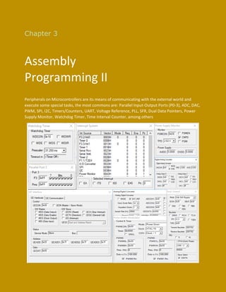
  • 14. The following program shows how to implement the UART communication, was tested with Tera Term UART Serial Interface Assembly Programming 12