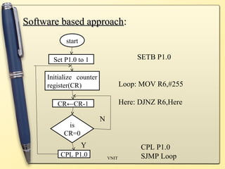
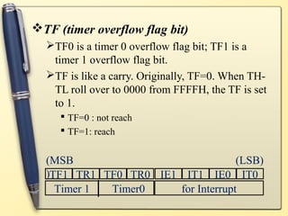
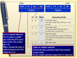
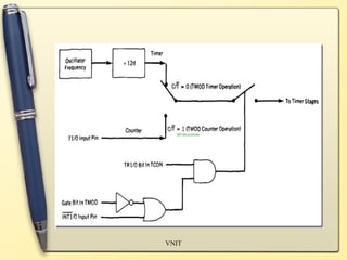
2. Introduction :
• To generate precise time delay and to count the
number of pulses timer / counter plays an
important role
Timer operations are basically three
types
1.software based approach
2. hardware based approach
3. combined software and hardware
approach
SJCET
3. SSooffttwwaarree bbaasseedd aapppprrooaacchh::
VNIT
start
Set P1.0 to 1
Initialize counter
register(CR)
CR←CR-1
is
CR=0
CPL P1.0
N
Y
SETB P1.0
Loop: MOV R6,#255
Here: DJNZ R6,Here
CPL P1.0
SJMP Loop
5. CCoommbbiinneedd SS//WW aanndd HH//WW aapppprrooaacchh :
Registers Used in Timers/Counters:
– TH0, TL0, TH1, TL1
– TMOD (Timer mode register)
– TCON (Timer control register)
SJCET
6. TTCCOONN RReeggiisstteerr
Timer control register: TCON
• Upper nibble for timer control, lower nibble for
interrupts
TR (run control bit)
• TR0 for Timer 0 control; TR1 for Timer 1 control.
• TR is set by programmer to turn timer/counter
on/off.
• TR=0: off (stop)
• TR=1: on (start)
(MSB) (LSB)
TF1 TR1 TF0 TR0 IE1 IT1 IE0 IT0
Timer 1 Timer0 for Interrupt
7. TF (timer overflow flag bit)
TF0 is a timer 0 overflow flag bit; TF1 is a
timer 1 overflow flag bit.
TF is like a carry. Originally, TF=0. When TH-TL
roll over to 0000 from FFFFH, the TF is set
to 1.
TF=0 : not reach
TF=1: reach
(MSB
)
(LSB)
TF1 TR1 TF0 TR0 IE1 IT1 IE0 IT0
Timer 1 Timer0 for Interrupt
9. TTMMOODD RReeggiisstteerr
Timer mode register: TMOD
• An 8-bit register
• Set the usage mode for two timers
• Set lower 4 bits for Timer 0 (Set to 0000
if not used)
• Set upper 4 bits for Timer 1 (Set to
0000 if not used)
• Not bit-addressable
(MSB) (LSB)
GATE C/T M1 M0 GATE C/T M1 M0
Timer 1 Timer 0
13. SStteeppss FFOORR TTIIMMEERRSS OOPPEERRAATTIIOONN
1. Choose mode 1 timer 0
MOV TMOD,#01H
1. Set the initiat value to TH0 and TL0.
MOV TH0,#FFH
MOV TL0,#FCH
1. Better to clear the flag to monitor: TF0=0.
CLR TF0
1. Start the timer.
SETB TR0
14. 5.The 8051 starts to count up by incrementing the TH0-TL0.
TH0-TL0= FFFCH,FFFDH,FFFEH,FFFFH,0000H
15. 6. When TH0-TL0 rolls over from FFFFH to
0000, the 8051 set TF0=1.
Now TF0=1
6. Keep monitoring the timer flag (TF) to see
if it is raised.
AGAIN: JNB TF0, AGAIN
6. Clear TR0 to stop the process.
CLR TR0
6. Clear the TF flag for the next round.
CLR TF0
16. Timer Delay CCaallccuullaattiioonn ffoorr XXTTAALL ==
1111..00559922 MMHHzz
(a) in hex
• (FFFF – YYXX ) × 1.085 ms
• where YYXX are TH, TL initial values
respectively.
• Notice that values YYXX are in hex.
(b) in decimal
• Convert YYXX values of the TH, TL register to
decimal to get a NNNNN decimal number
• then (65536 – NNNNN) × 1.085 ms
17. • Assume that XTAL = 11.0592 MHz .
• And we know desired delay
• how to find the values for the TH,TL ?
1. Divide the delay by 1.085 ms and get n.
2. Perform 65536 –n
3. Convert the result of Step 2 to hex ( yyxx)
4. Set TH = yy and TL = xx.
18. Example 1:
• Assuming XTAL = 11.0592 MHz,
• write a program to generate a square wave of 50 Hz
frequency on pin P2.3.
Solution:
1. The period of the square wave = 1 / 50 Hz = 20
ms.
2. The high or low portion of the square wave = 10
ms.
3. 10 ms / 1.085 ms = 9216
4. 65536 – 9216 = 56320 in decimal = DC00H in
hex.
5. TL1 = 00H and TH1 = DCH.
20. Example 2:
square wave of 50% duty on P1.5
Timer 0 is used
;each loop is a half clock
MOV TMOD,#01 ;Timer 0,mode 1(16-bit)
HERE: MOV TL0,#0F2H ;Timer value = FFF2H
MOV TH0,#0FFH
CPL P1.5
ACALL DELAY
SJMP HERE
50% 50%
whole clock
P1.5