Downloaded 70 times


![Introduction
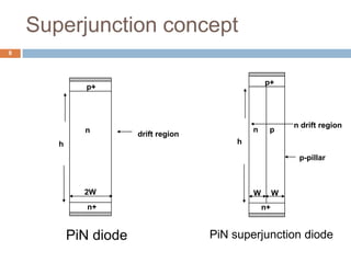
In conventional power devices, there is a well known trade-
off between specific on resistance and breakdown voltage [1]
The idea of a superjunction has been used to improve this
relationship from power law to linear [2]
[1] C. Hu, “Optimum doping profile for minimum ohmic resistance and high breakdown
voltage,” IEEE Trans Electron Devices, Vol.ED-26, pp.243-245, Mar. 1979.
[2] Jian Chen, Weifeng Sun et al, “A Review of Superjunction Vertical Diffused MOSFET”,
IETE Technical review, Vol29, Issue1, Jan-Feb 2012.
5.2
BVRonsp
5](https://image.slidesharecdn.com/m120128ec-131008045741-phpapp01/85/SUPERJUNCTION-IN-Silicon-Carbide-Diodes-5-320.jpg)
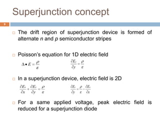
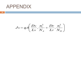
![How breakdown occurs?
BV of a power device is an important parameter
governing reverse blocking capability
How breakdown occurs?
Impact ionization, a multiplicative phenomenon leads
to avalanche of carriers when breakdown voltage is
reached
BV and ND (donor concentration in the uniformly doped
n region) relation in a P+N diode is given by [3]
4/315
100.3)4( DNSiCHBV
6
[3] B.J. Baliga, “Breakdown Voltage,” in Silicon Carbide Power Devices, World Scientific Publishing,
Singapore 2005, pp. 42-43](https://image.slidesharecdn.com/m120128ec-131008045741-phpapp01/85/SUPERJUNCTION-IN-Silicon-Carbide-Diodes-6-320.jpg)
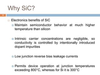
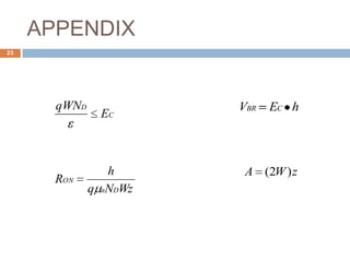
![Specific on resistance
Inverse relation between Ronsp and ND in a P+N diode is
given by[3]
A higher Ronsp adversely affects the performance of the
device by increasing conducting loss and lowering
switching speed
In conventional power devices the ideal trade-off
between Ronsp and BV
Dn
D
onsp
Nq
W
R
5.2
BVRonsp Si limit
7
[3] B.J. Baliga, “Breakdown Voltage,” in Silicon Carbide Power Devices, World Scientific Publishing,
Singapore 2005, pp. 42-43](https://image.slidesharecdn.com/m120128ec-131008045741-phpapp01/85/SUPERJUNCTION-IN-Silicon-Carbide-Diodes-7-320.jpg)

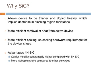
![MATERIAL PARAMETERS
11
MATERIAL 6H-
SiC
4H-
SiC
3C-
SiC
Si GaAs
Dielectric constant 9.66 9.7 9.72 11.8 13.1
Band gap(eV) at 300K 3.0 3.2 2.3 1.1 1.42
Intrinsic carrier concentration(cm-3) 10-5 10-7 10 1010 1.8*106
Mobility(μn)(cm2/Vs)
ND=1016 cm-3
par:60
per:400
par:800
per:800
750 1200 6500
Mobility(μp)(cm2/Vs)
ND=1016 cm-3
90 115 40 420 320
Breakdown field (MVcm-1)
at ND=1017 cm-3
par:3.2
per: >1
par:3.0 >1.5 0.6 0.6
Thermal conductivity(Wcm-1K-1) 3-5 3-5 3-5 1.5 0.5
[4] http://www.tf.uni-](https://image.slidesharecdn.com/m120128ec-131008045741-phpapp01/85/SUPERJUNCTION-IN-Silicon-Carbide-Diodes-11-320.jpg)
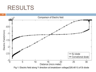
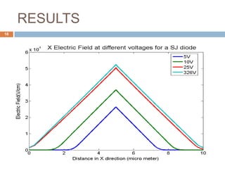

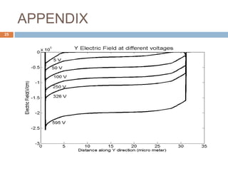

This document summarizes a study of a 4H-SiC superjunction power diode through simulation. It discusses the methodology, which involves a literature survey and simulations using semiconductor simulation software. It provides an introduction to superjunction concepts and comparisons between different materials like SiC and Si. The results section shows electric field simulations of Si diodes with and without superjunction structures. The work plan is to extend the simulations to 4H-SiC diodes and later to SiC MOSFETs.