Recommended
PPTX
Silicon on Insulator (SOI) Technology
PDF
PPTX
Advanced CMOS on Silicon-On-Insulator (SOI) Technology for High-Performance V...
PPTX
PPTX
PDF
Silicon-On-Insulator (SOI) Technology: Fabrication, Device Effects & Advanced...
PDF
PPTX
Its regarding SOI technique. Sillicon on insulator.
PPTX
Ultra-thin body SOI MOSFETs: Term Paper_class presentation on Advanced topics...
PDF
Performance_Evaluation_of_Fully_Depleted_Silicon_on_Insulator_MOSFET.pdf
PPTX
PPTX
PDF
FABRICATION OF BICMOS ON SILICON AND SOI
PPTX
Fully depleted silicon insulator
PPT
3. CMOS Fabrication.ppt important to read
PPT
PPTX
workjnuuuuuuuuuuuooooooooooooooooooouuuuuuuuuuuuuuuuuuuuuuuuuu]]
PDF
FUNDAMENTALS_of_CMOS_VLSI_5th_SEM_ECE.pdf
PDF
Soi cmos device technology
PPT
PPTX
Silicon on Insulator Introduction (Semiconductor Devices).pptx
PPTX
MOSFET, SOI-FET and FIN-FET-ABU SYED KUET
PDF
vlsi12312313123123123123123123123123123123.pdf
PPTX
EEE498_Thesis_Presentation.pptx that it is 12
PDF
Patented solution to improve ESD robustness of SOI MOS transistors
PPTX
Metal oxide-semiconductorfetmosfet-090615015822-phpapp02
PPTX
MOSFET(ABOUT,FABRICATION)
PDF
PPTX
Basin Design Service, LLC Introduction Presentation
PPTX
ISO 13485.2016 Awareness's Training material
More Related Content
PPTX
Silicon on Insulator (SOI) Technology
PDF
PPTX
Advanced CMOS on Silicon-On-Insulator (SOI) Technology for High-Performance V...
PPTX
PPTX
PDF
Silicon-On-Insulator (SOI) Technology: Fabrication, Device Effects & Advanced...
PDF
PPTX
Its regarding SOI technique. Sillicon on insulator.
Similar to Its regarding Silicon on Insulator technique
PPTX
Ultra-thin body SOI MOSFETs: Term Paper_class presentation on Advanced topics...
PDF
Performance_Evaluation_of_Fully_Depleted_Silicon_on_Insulator_MOSFET.pdf
PPTX
PPTX
PDF
FABRICATION OF BICMOS ON SILICON AND SOI
PPTX
Fully depleted silicon insulator
PPT
3. CMOS Fabrication.ppt important to read
PPT
PPTX
workjnuuuuuuuuuuuooooooooooooooooooouuuuuuuuuuuuuuuuuuuuuuuuuu]]
PDF
FUNDAMENTALS_of_CMOS_VLSI_5th_SEM_ECE.pdf
PDF
Soi cmos device technology
PPT
PPTX
Silicon on Insulator Introduction (Semiconductor Devices).pptx
PPTX
MOSFET, SOI-FET and FIN-FET-ABU SYED KUET
PDF
vlsi12312313123123123123123123123123123123.pdf
PPTX
EEE498_Thesis_Presentation.pptx that it is 12
PDF
Patented solution to improve ESD robustness of SOI MOS transistors
PPTX
Metal oxide-semiconductorfetmosfet-090615015822-phpapp02
PPTX
MOSFET(ABOUT,FABRICATION)
PDF
Recently uploaded
PPTX
Basin Design Service, LLC Introduction Presentation
PPTX
ISO 13485.2016 Awareness's Training material
PDF
Shear Strength of Soil/Mohr Coulomb Failure Criteria-1.pdf
PPTX
Distresses in Road Flexible pavement.pptx
PPT
L9_Statistical Evaluation of Measurement Data.ppt
PPTX
Unit 3_statistical methods in data science.pptx
PPTX
SketchUp Pro 2026 – Advanced 3D Modeling Software
PPTX
Integrating Azure Event Services_ Event Grid, Event Hubs, and Service Bus.pptx
PDF
Computer Graphics Fundamentals (v0p1) - DannyJiang
PPTX
mtbf mttr modeling maintenance engineering
PDF
CME397 SURFACE ENGINEERING UNIT 2 FULL NOTES
PPTX
Why TPM Succeeds in Some Plants and Struggles in Others | MaintWiz
PDF
Module 4 python programming-1BPLCK105B-2025 by Dr.SV.pdf
PPTX
How Does LNG Regasification Work | INOXCVA
PDF
comprehensive analysis of cross-chain bridges in the DeFi - Garima Singh
PDF
Fire fighting arrangement in public assembly buildings
PPTX
We-Optimized-Everything-Except-Decision-Quality-Maintenance-MaintWiz.pptx
PPTX
Introduction to AI and Applications Module-4.pptx
PPT
Momentum and collisions in physics or engineering
PDF
Chris Elwell Woburn - An Experienced IT Executive
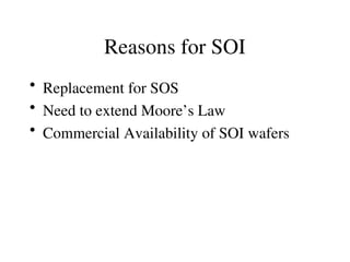
Its regarding Silicon on Insulator technique 1. 2. Reasons for SOI
• Replacement for SOS
• Need to extend Moore’s Law
• Commercial Availability of SOI wafers
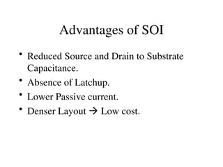
3. Advantages of SOI
• Reduced Source and Drain to Substrate
Capacitance.
• Absence of Latchup.
• Lower Passive current.
• Denser Layout Low cost.
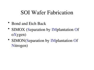
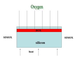
4. SOI Wafer Fabrication
• Bond and Etch Back
• SIMOX (Separation by IMplantation Of
oXygen)
• SIMON(Separation by IMplantation Of
Nitrogen)
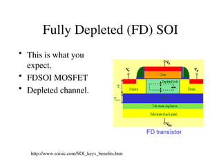
5. 6. Fully Depleted (FD) SOI
• This is what you
expect.
• FDSOI MOSFET
• Depleted channel.
http://www.soisic.com/SOI_keys_benefits.htm
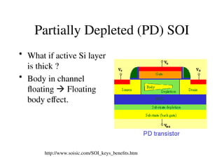
7. Partially Depleted (PD) SOI
• What if active Si layer
is thick ?
• Body in channel
floating Floating
body effect.
http://www.soisic.com/SOI_keys_benefits.htm
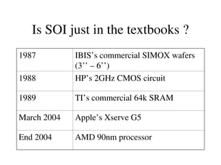
8. Is SOI just in the textbooks ?
1987 IBIS’s commercial SIMOX wafers
(3’’ – 6’’)
1988 HP’s 2GHz CMOS circuit
1989 TI’s commercial 64k SRAM
March 2004 Apple’s Xserve G5
End 2004 AMD 90nm processor
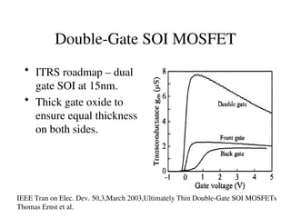
9. 10. Double-Gate SOI MOSFET
• ITRS roadmap – dual
gate SOI at 15nm.
• Thick gate oxide to
ensure equal thickness
on both sides.
IEEE Tran on Elec. Dev. 50,3,March 2003,Ultimately Thin Double-Gate SOI MOSFETs
Thomas Ernst et al.
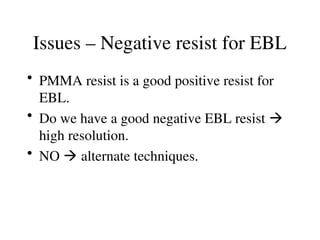
11. Issues – Negative resist for EBL
• PMMA resist is a good positive resist for
EBL.
• Do we have a good negative EBL resist
high resolution.
• NO alternate techniques.
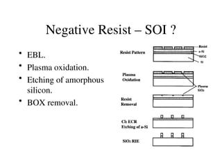
12. Negative Resist – SOI ?
• EBL.
• Plasma oxidation.
• Etching of amorphous
silicon.
• BOX removal.
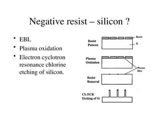
13. Negative resist – silicon ?
• EBL
• Plasma oxidation
• Electron cyclotron
resonance chlorine
etching of silicon.
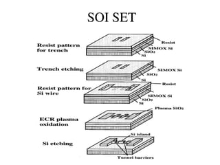
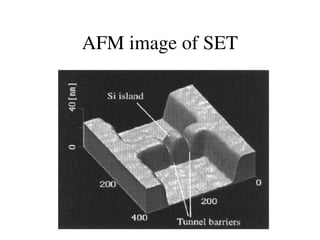
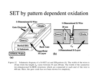
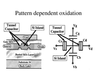
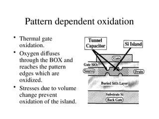
14. 15. 16. 17. 18. 19. 20. Pattern dependent oxidation
• Thermal gate
oxidation.
• Oxygen diffuses
through the BOX and
reaches the pattern
edges which are
oxidized.
• Stresses due to volume
change prevent
oxidation of the island.
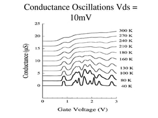
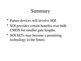
21. 22. 23. 24. 25. Summary
• Future devices will involve SOI.
• SOI provides certain benefits over bulk
CMOS for smaller gate lengths.
• SOI SETs may become a promising
technology in the future.


![workjnuuuuuuuuuuuooooooooooooooooooouuuuuuuuuuuuuuuuuuuuuuuuuu]]](https://cdn.slidesharecdn.com/ss_thumbnails/baippdtcblop01fie-251222045342-5aabffab-thumbnail.jpg?width=640&height=640&fit=bounds)