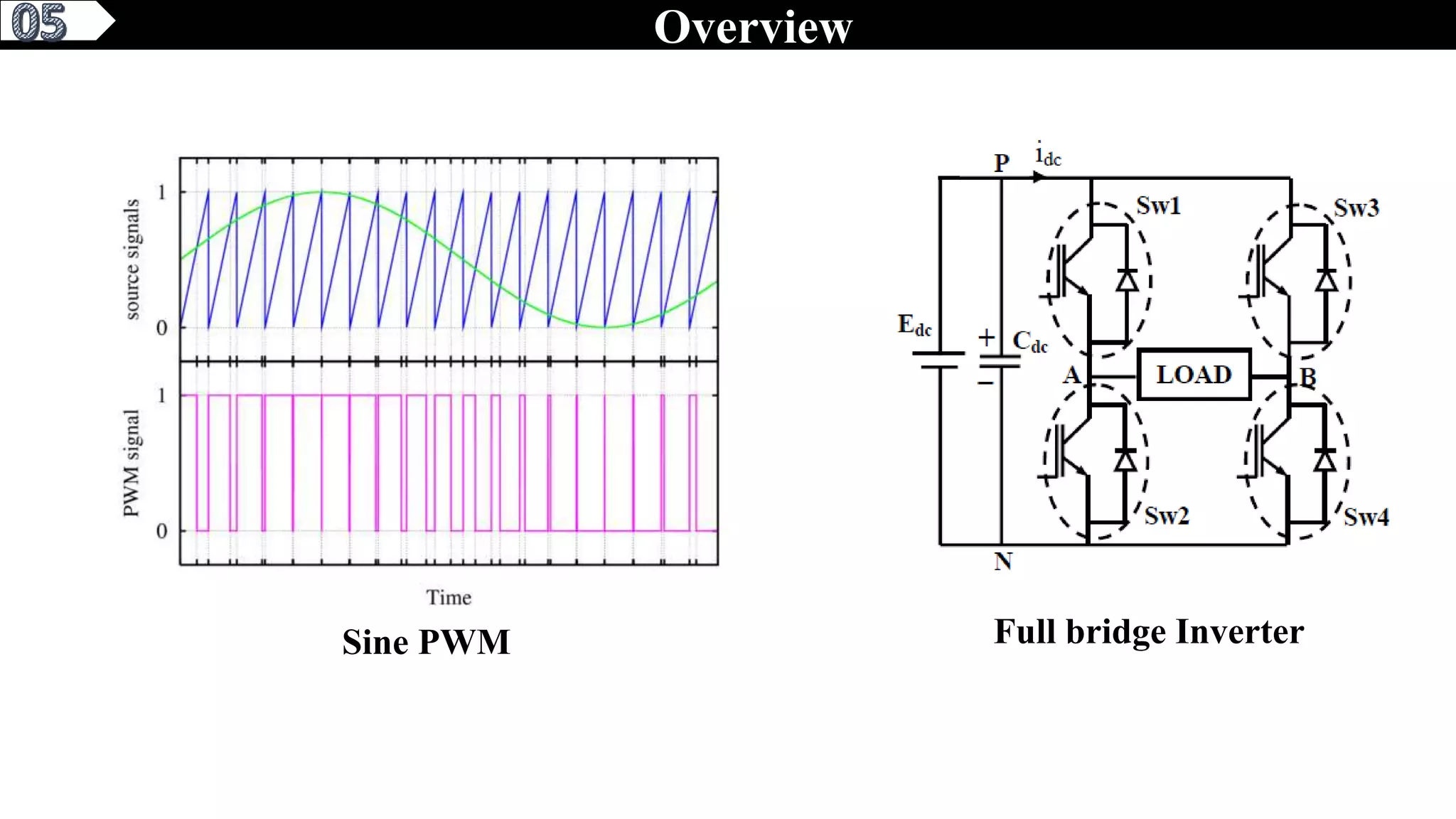
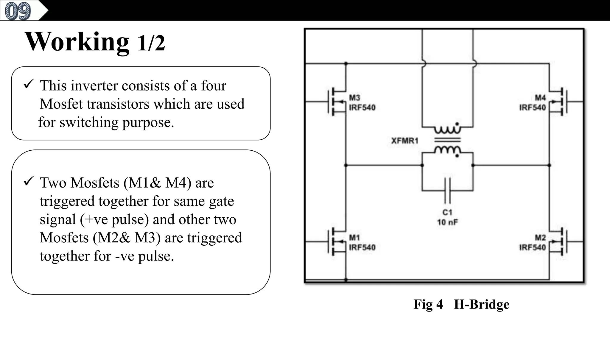
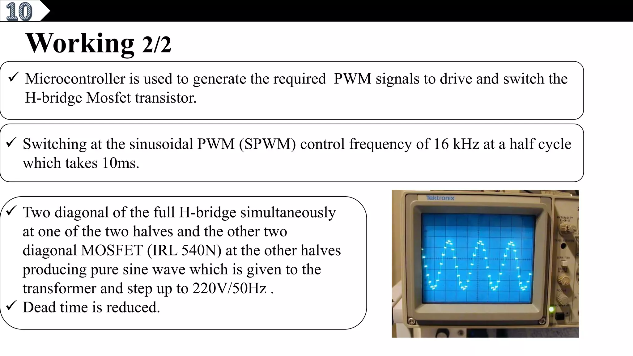
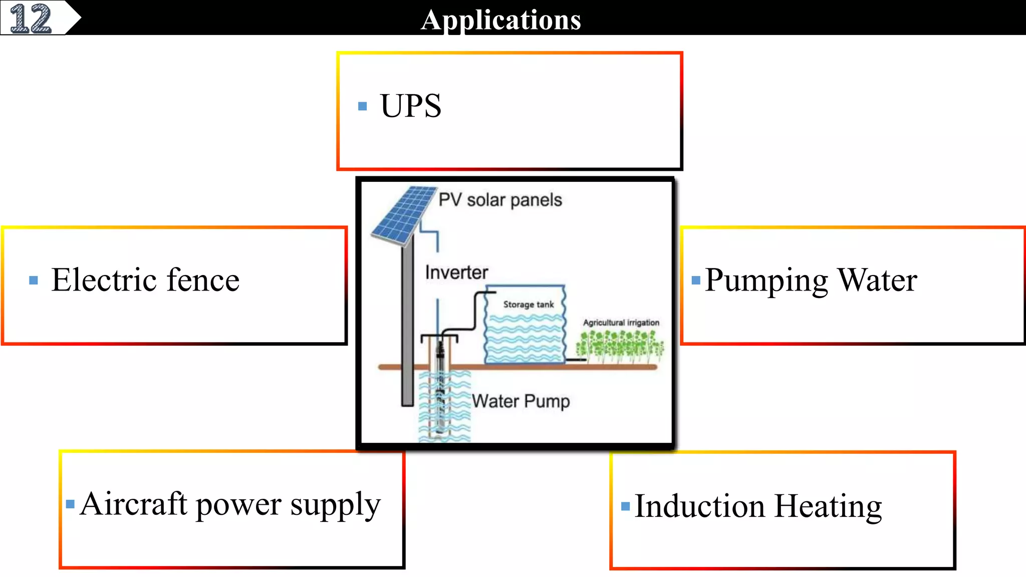
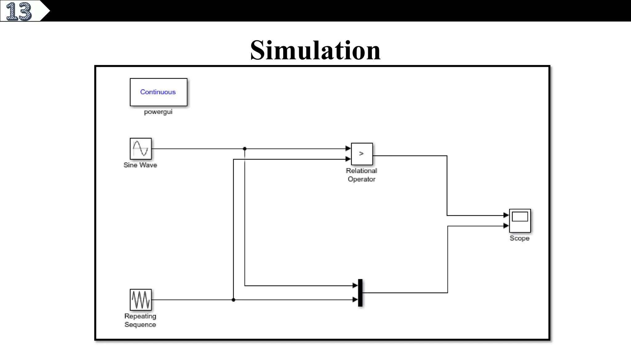
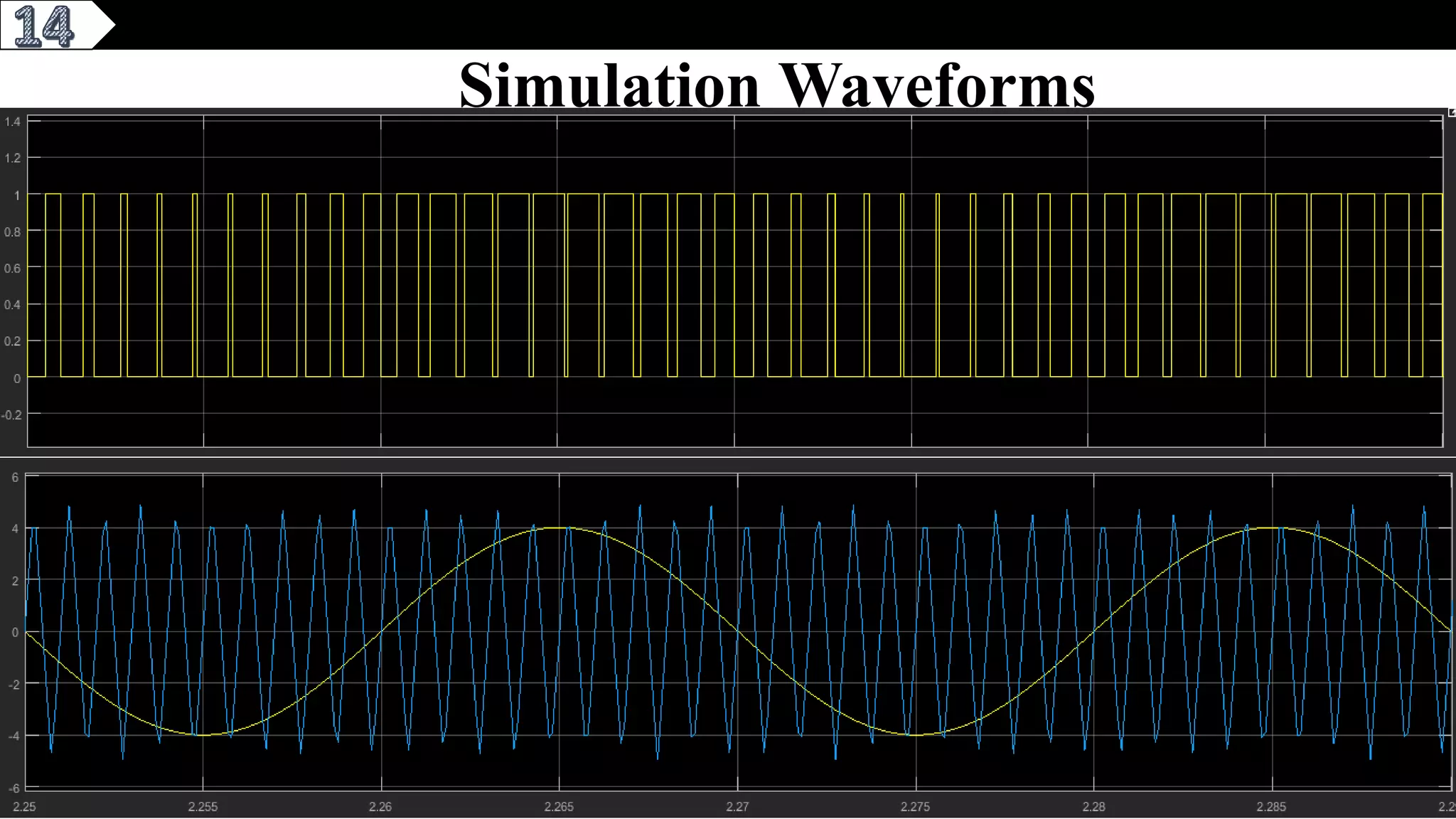
Pure Sine Wave Single Phase Inverter
Abuzar Uzair Hasnain Hamza Hummayun
SP15-BEE-096 SP15-BEE-106 SP15-BEE-100 SP15-BEE-029 SP15-BEE-127
Contents
3
1. Problem Statement.
2. Introduction.
6. Working.
3. Components.
4. Block Diagram.
5. Circuit Diagram.
7. Advantages.
8. Applications.
9. Simulation.
3
Problem Statement
Square wave inverter produces greater number of
harmonics which produces heating effect and can
results in damage of our electronic appliances.
Fig 1 SPWM
Introduction
 Sine Pulse Width Modulation (SPWM)
switching technique is used.
 Conversion from the DC-to-AC.
 It is widely used in power electronic
applications.
 Comparison of reference sine signal with
carrier signal.
 When reference signal is greater than
carrier switch is will be on.
3
Sine PWM Full bridge Inverter
Overview
Working 7
S.no Components
01 Transformer
02 Microcontroller
03 DC Supply
04 Mosfet
05 Capacitor
06 Gate Drive IC
Table 01: Components
Block Diagram
8
Fig 2 Block diagram of Pure SineWave Inverter
Circuit Diagram
9
Fig 3 Circuit Diagram of Pure Sine Wave Inverter.
6
Working 1/2
 This inverter consists of a four
Mosfet transistors which are used
for switching purpose.
 Two Mosfets (M1& M4) are
triggered together for same gate
signal (+ve pulse) and other two
Mosfets (M2& M3) are triggered
together for -ve pulse.
Fig 4 H-Bridge
6
Working 2/2
 Microcontroller is used to generate the required PWM signals to drive and switch the
H-bridge Mosfet transistor.
 Switching at the sinusoidal PWM (SPWM) control frequency of 16 kHz at a half cycle
which takes 10ms.
 Two diagonal of the full H-bridge simultaneously
at one of the two halves and the other two
diagonal MOSFET (IRL 540N) at the other halves
producing pure sine wave which is given to the
transformer and step up to 220V/50Hz .
 Dead time is reduced.
Advantages
 Reduces the number of
harmonics.
 Attain the optimum
dead time.
 Increases the overall
effeciency.
 Producing pure sinusoidal
wave .
 Increases the Vrms value
of the system.
Advantages
17
Applications
 Electric fence Pumping Water
Aircraft power supply Induction Heating
 UPS
Applications
3
Simulation
3
Simulation Waveforms
3
Conclusion
o The SPWM technique is used to control the inverter switch. This
method is superior to other methods because it improves the
quality of the output waveform.
o The dead time is reduced from 180μs to 63μs which increases the
overall Vrms.
o The efficiency of the inverter is increased to large extent due to
pure sine wave at output which reduces total harmonic distortion
(THD).
Thank You !!!

Sine wave inverter

  • 2.
    Pure Sine WaveSingle Phase Inverter Abuzar Uzair Hasnain Hamza Hummayun SP15-BEE-096 SP15-BEE-106 SP15-BEE-100 SP15-BEE-029 SP15-BEE-127
  • 3.
    Contents 3 1. Problem Statement. 2.Introduction. 6. Working. 3. Components. 4. Block Diagram. 5. Circuit Diagram. 7. Advantages. 8. Applications. 9. Simulation.
  • 4.
    3 Problem Statement Square waveinverter produces greater number of harmonics which produces heating effect and can results in damage of our electronic appliances.
  • 5.
    Fig 1 SPWM Introduction Sine Pulse Width Modulation (SPWM) switching technique is used.  Conversion from the DC-to-AC.  It is widely used in power electronic applications.  Comparison of reference sine signal with carrier signal.  When reference signal is greater than carrier switch is will be on.
  • 6.
    3 Sine PWM Fullbridge Inverter Overview
  • 7.
    Working 7 S.no Components 01Transformer 02 Microcontroller 03 DC Supply 04 Mosfet 05 Capacitor 06 Gate Drive IC Table 01: Components
  • 8.
    Block Diagram 8 Fig 2Block diagram of Pure SineWave Inverter
  • 9.
    Circuit Diagram 9 Fig 3Circuit Diagram of Pure Sine Wave Inverter.
  • 10.
    6 Working 1/2  Thisinverter consists of a four Mosfet transistors which are used for switching purpose.  Two Mosfets (M1& M4) are triggered together for same gate signal (+ve pulse) and other two Mosfets (M2& M3) are triggered together for -ve pulse. Fig 4 H-Bridge
  • 11.
    6 Working 2/2  Microcontrolleris used to generate the required PWM signals to drive and switch the H-bridge Mosfet transistor.  Switching at the sinusoidal PWM (SPWM) control frequency of 16 kHz at a half cycle which takes 10ms.  Two diagonal of the full H-bridge simultaneously at one of the two halves and the other two diagonal MOSFET (IRL 540N) at the other halves producing pure sine wave which is given to the transformer and step up to 220V/50Hz .  Dead time is reduced.
  • 12.
    Advantages  Reduces thenumber of harmonics.  Attain the optimum dead time.  Increases the overall effeciency.  Producing pure sinusoidal wave .  Increases the Vrms value of the system. Advantages
  • 13.
    17 Applications  Electric fencePumping Water Aircraft power supply Induction Heating  UPS Applications
  • 14.
  • 15.
  • 16.
    3 Conclusion o The SPWMtechnique is used to control the inverter switch. This method is superior to other methods because it improves the quality of the output waveform. o The dead time is reduced from 180μs to 63μs which increases the overall Vrms. o The efficiency of the inverter is increased to large extent due to pure sine wave at output which reduces total harmonic distortion (THD).
  • 17.