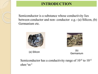
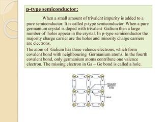
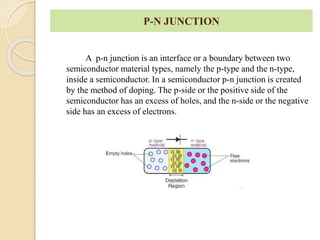
Semiconductor
Presented By: DETSUNG BARO
: MWIKHUM BASUMATARY
CONTENTS
1. Introduction
2. Band Theory
3.Types of Semiconductor
4. Doping
5 . P-N junction
7. Usage of semiconductor
8
INTRODUCTION
Semiconductor has a conductivity range of 10-6 to 10-4
ohm-1m-1
(a) Silicon
(b)
Germanium
Semiconductor is a substance whose conductivity lies
between conductor and non- conductor e.g.- (a) Silicon, (b)
Germanium etc.
BAND THEORY
In solids the molecules are closely arranged together, due to this the
atoms of molecules tend to move into the orbitals of neighbouring atoms.So
several bands of energy levels are formed due to the intermixing of atoms
in solids. We call these set of energy levels as energy bands.
Classification of Energy Bands:
Valence Band:
The electrons in the outermost shell are known as valence electrons.
These valence electrons contain a series of energy levels and form an
energy band known as valence band. The valence band has the highest
occupied energy.
Conduction Band
The valence electrons are not tightly held to the nucleus due to which
a few of these valence electrons leave the outermost orbit even at room
temperature and become free electrons. The free electrons conduct current
in conductors and are therefore known as conduction electrons. The
conduction band is one that contains conduction electrons and has the
lowest occupied energy levels.
Forbidden Energy Gap
The gap between the valence band and the conduction band is
referred to as forbidden gap. As the name suggests, the forbidden gap
doesn’t have any energy and no electrons stay in this band. If the forbidden
energy gap is greater, then the valence band electrons are tightly bound or
firmly attached to the nucleus. We require some amount of external energy
that is equal to the forbidden energy gap.
As shown in figure above the forbidden gap in case of conductors are
very small (0 eV ), so electrons can move easily from valence band to
conduction band.
In case of insulators the forbidden gap is so large ( 5eV or more) that
irrespective of energy provided, electron cannot jump from valence band to
conduction band.
And in semiconductor the forbidden gap is smaller than the insulator but
larger than the conductor (for silicon 1.1 eV and for germanium 0.7 eV).
TYPES
Instrinsic : A semiconductor in an extremely pure form is called
instrinsic semiconducter
Extrinsic : When a small amount of suitable impurity (by doping) is
added to a semiconductor,it is called an enstrinsic semiconductor
SEMICONDUCTOR
INTRINSIC
SEMICONDUCTOR
EXTRINSIC
SEMICONDUCTOR
Doping: The process of adding some impurity atoms in a pure or intrinsic
semiconductor so as to increase the conductivity of a semiconductor is called doping.
Depending upon the types of impurities extrinsic semiconductor are classified into two types-
 n-type
p-type
n-type semiconductor:
When a small amount of pentavelent impurity is added to a pure semiconductor, it is called
n-type semiconductor. Addition of pentavalent impurity provides a large number of free
electrons in semiconductor crystal. In n-type semiconductor the majority charge carrier are
free electrons and minority charge carriers are holes.
Doping
p-type semiconductor:
When a small amount of trivalent impurity is added to a
pure semiconductor. It is called p-type semiconductor. When a pure
germanium crystal is doped with trivalent Galium then a large
number of holes appear in the crystal. In p-type semiconductor the
majority charge carrier are the holes and minority charge carriers
are electrons.
The atom of Galium has three valence electrons, which form
covalent bond with neighbouring Germanium atoms. In the fourth
covalent bond, only germanium atoms contribute one valence
electron. The missing electron in Ga – Ge bond is called a hole.
P-N JUNCTION
A p-n junction is an interface or a boundary between two
semiconductor material types, namely the p-type and the n-type,
inside a semiconductor. In a semiconductor p-n junction is created
by the method of doping. The p-side or the positive side of the
semiconductor has an excess of holes, and the n-side or the negative
side has an excess of electrons.
When p-n junction is formed then electrons in n-side semiconductor
starts diffusing into the p-side. Thus having the positive charges near5 the
p-n junction simultaneously holes in p-type starts diffusing into the n-type
thus having negative charges near the p-n junction. Simultaneously holes
in p-type starts diffusing into the n-type thus having negative charges near
the p-n junction. These two layers of +ve and –ve charges form the
depletion layer.
The +ve and –ve charges near the p-n junction produces an electric
field. The electric field is a barrier to the free electron in the n-type region.
There exist a potential difference across the depletion layer and is called
potential barrier.
Uses of semi conductors
Semiconductors are mostly used in every sector of electronics
e.g.-
 Temperature sensors are made of semiconductor
 It is used in 3d printing.
 It is used in microchips and self driving car.
 Used in calculators, solar plates, computers and other electronic
devices.
 Transistor and MOSFET used in electrical circuits switch are
manufactured using the semiconductors.
THANK YOU

Semiconductor.pptx

  • 1.
    Semiconductor Presented By: DETSUNGBARO : MWIKHUM BASUMATARY
  • 2.
    CONTENTS 1. Introduction 2. BandTheory 3.Types of Semiconductor 4. Doping 5 . P-N junction 7. Usage of semiconductor 8
  • 3.
    INTRODUCTION Semiconductor has aconductivity range of 10-6 to 10-4 ohm-1m-1 (a) Silicon (b) Germanium Semiconductor is a substance whose conductivity lies between conductor and non- conductor e.g.- (a) Silicon, (b) Germanium etc.
  • 4.
    BAND THEORY In solidsthe molecules are closely arranged together, due to this the atoms of molecules tend to move into the orbitals of neighbouring atoms.So several bands of energy levels are formed due to the intermixing of atoms in solids. We call these set of energy levels as energy bands. Classification of Energy Bands: Valence Band: The electrons in the outermost shell are known as valence electrons. These valence electrons contain a series of energy levels and form an energy band known as valence band. The valence band has the highest occupied energy.
  • 5.
    Conduction Band The valenceelectrons are not tightly held to the nucleus due to which a few of these valence electrons leave the outermost orbit even at room temperature and become free electrons. The free electrons conduct current in conductors and are therefore known as conduction electrons. The conduction band is one that contains conduction electrons and has the lowest occupied energy levels. Forbidden Energy Gap The gap between the valence band and the conduction band is referred to as forbidden gap. As the name suggests, the forbidden gap doesn’t have any energy and no electrons stay in this band. If the forbidden energy gap is greater, then the valence band electrons are tightly bound or firmly attached to the nucleus. We require some amount of external energy that is equal to the forbidden energy gap.
  • 6.
    As shown infigure above the forbidden gap in case of conductors are very small (0 eV ), so electrons can move easily from valence band to conduction band. In case of insulators the forbidden gap is so large ( 5eV or more) that irrespective of energy provided, electron cannot jump from valence band to conduction band. And in semiconductor the forbidden gap is smaller than the insulator but larger than the conductor (for silicon 1.1 eV and for germanium 0.7 eV).
  • 7.
    TYPES Instrinsic : Asemiconductor in an extremely pure form is called instrinsic semiconducter Extrinsic : When a small amount of suitable impurity (by doping) is added to a semiconductor,it is called an enstrinsic semiconductor SEMICONDUCTOR INTRINSIC SEMICONDUCTOR EXTRINSIC SEMICONDUCTOR
  • 8.
    Doping: The processof adding some impurity atoms in a pure or intrinsic semiconductor so as to increase the conductivity of a semiconductor is called doping. Depending upon the types of impurities extrinsic semiconductor are classified into two types-  n-type p-type n-type semiconductor: When a small amount of pentavelent impurity is added to a pure semiconductor, it is called n-type semiconductor. Addition of pentavalent impurity provides a large number of free electrons in semiconductor crystal. In n-type semiconductor the majority charge carrier are free electrons and minority charge carriers are holes. Doping
  • 9.
    p-type semiconductor: When asmall amount of trivalent impurity is added to a pure semiconductor. It is called p-type semiconductor. When a pure germanium crystal is doped with trivalent Galium then a large number of holes appear in the crystal. In p-type semiconductor the majority charge carrier are the holes and minority charge carriers are electrons. The atom of Galium has three valence electrons, which form covalent bond with neighbouring Germanium atoms. In the fourth covalent bond, only germanium atoms contribute one valence electron. The missing electron in Ga – Ge bond is called a hole.
  • 10.
    P-N JUNCTION A p-njunction is an interface or a boundary between two semiconductor material types, namely the p-type and the n-type, inside a semiconductor. In a semiconductor p-n junction is created by the method of doping. The p-side or the positive side of the semiconductor has an excess of holes, and the n-side or the negative side has an excess of electrons.
  • 11.
    When p-n junctionis formed then electrons in n-side semiconductor starts diffusing into the p-side. Thus having the positive charges near5 the p-n junction simultaneously holes in p-type starts diffusing into the n-type thus having negative charges near the p-n junction. Simultaneously holes in p-type starts diffusing into the n-type thus having negative charges near the p-n junction. These two layers of +ve and –ve charges form the depletion layer. The +ve and –ve charges near the p-n junction produces an electric field. The electric field is a barrier to the free electron in the n-type region. There exist a potential difference across the depletion layer and is called potential barrier.
  • 12.
    Uses of semiconductors Semiconductors are mostly used in every sector of electronics e.g.-  Temperature sensors are made of semiconductor  It is used in 3d printing.  It is used in microchips and self driving car.  Used in calculators, solar plates, computers and other electronic devices.  Transistor and MOSFET used in electrical circuits switch are manufactured using the semiconductors.
  • 13.