Scanning acoustic microscopy (SAM) is a non-destructive technique that uses ultrasound to examine the internal structure and surfaces of materials. The document discusses several case studies where SAM was used successfully for failure analysis, including detecting missing underfill material in flip chip devices, delamination between layers in round electronics, voids in solder mask coatings, and delamination in obsolete components. SAM provided high resolution imaging to identify these issues internally in a non-destructive manner and more efficiently than alternative destructive techniques such as cross-sectioning. The case studies demonstrate how SAM can be applied practically for reliability testing and failure analysis in microelectronics.
Pad Cratering: Prevention, Mitigation and Detection StrategiesCheryl Tulkoff
Pad cratering is defined as cracking which initiates within the laminate during a dynamic mechanical event such as In Circuit Testing (ICT), board depanelization, connector insertion, and other shock and vibration inducing activities.
During this tutorial, you'll learn about the key drivers, measurement and detection protocols, and preventive tactics for this serious but prevalent failure. Pad cratering was first recognized in BGA packages but newer leadless, bottom termination components are also vulnerable.
Unit-III Non Destructive Testing (NDT)
Subject Name: OML751 Testing of Materials
Topics: Various NDT tests [Visual inspection, Liquid penetrant test, Magnetic particle test, Thermography test, Radiographic test, Eddy current test, Ultrasonic test, Acoustic emission test]
B.E. Mechanical Engineering
Final Year, VII Semester, Open Elective Subject
[As per Anna University R-2017]
Metal Additive Manufacturing - Basics Zero to One - June 2018bMatthew Burris
A brief on metal additive manufacturing. Covering the hype, realities, industry growth, where companies have found value with metal additive manufacturing, the value levers of metal additive manufacturing with case studies, and considerations of adopting metal additive manufacturing.
Detailed illustration of MSA procedures both for Variable and attribute, Analysis of results and planning for MSA. Complete guidance for planning and implementation of MSA.
This is to prepare training course material for new onboard fellow workers who interest in failure analysis technique of semiconductor IC. Some irrelevant parameters, names, dates, and details have been removed for better understanding and focus on key considerations.In this report, a lot of attention is given to establishing the thinking process and experience-based instinct. This is one of best failure analysis reports I have ever working alone and excellent ideas from third party laboratories and test program compilers. What makes the failure analysis distinct is innovative skill and knowledge of physical/chemical theory. Accumulation of tons of failure analysis experience grows good quality instinct determining how effective process will be.Cheers,CH Shen
What is Six Sigma?,Methodology of Six sigma, What Six Sigma involve? , Why to adopt Six sigma?, Six sigma levels, Advantages of Six Sigma?, Disadvantages of Six Sigma?, Six Sigma Companies
7 QC Tools PDF | An eBook with A Detailed Description and Practical ExamplesShakehand with Life
Follow the link https://payhip.com/b/VCtH to download the complete eBook of '7 QC Tools PDF.
Train yourself and be the master of 7 QC Tools with this eBook of 7 QC Tools in PDF with a detailed description and illustrative examples of all 7 Quality Control Tools. Learn to construct the Histogram, Pareto Chart, Scatter Chart, Control Charts in Excel and analyze the data in Excel.
Tensile testing is one method routinely used to determine the mechanical properties of plastics. This piece presents an example of measuring the mechanical properties of acrylonitrile butadiene styrene (ABS), Polyoxymethylene (POM), Polyethylene terephthalate (PET) and polystyrene (PS)
What is MSA .
1. Why we Need MSA
2. How to use data.
3.Measurement Error Sources of Variation
• Precision (Resolution, Repeat ability, Reproducibility)
•Accuracy (Bias, Stability, Linearity)
4.What is Gage R&R?
5.Explain MSA Sheet
Advantages of Eddy Current Array over Magnetic Particle and Penetrant Testing...Olympus IMS
The use of eddy current array (ECA) technology has already been shown to increase the speed of inspections and the reliability of the surface inspection process. However, inspecting the surface of the carbon steel welds used in pipelines and pressure vessels represents many challenges for this technology. The geometric shape of the weld crown, the paint thickness, the presence of crest and crowns, and the ferromagnetism of the carbon steel are constraints. New tools have recently been developed to help overcome these challenges. A new orthogonal-type ECA probe based on flexible printed circuit board (PCB) technology conforms to the shape of the weld to help ensure flaw detection. Dynamic lift-off compensation and depth sizing tools were then added to a modern flaw detector, resulting in a leading-edge solution that can potentially replace magnetic particle testing for carbon steel weld inspection. With these inspection tools, users can fully benefit from the portability, imaging, data archiving, and reporting capabilities of eddy current array instruments. In this presentation, we review this new carbon weld inspection solution and present results that demonstrate the solution’s effectiveness for inspecting carbon steel welds. This information is technically advanced and is addressed to NDT operators and engineers.
Presenter:
Tommy Bourgelas
Olympus NDT Canada – A subsidiary of Olympus Scientific Solutions Americas, Inc.
Product Manager, Eddy Current and Bond Testing product line
Tommy has worked for Olympus NDT, formerly known as R/D Tech, for 16 years. Prior to his current position as Product Manager for eddy current testing and bond testing products, he worked to develop eddy current and bond testing applications, improve existing products, develop new products, and has trained numerous individuals on ECA and bond testing technology.
Abstract: Additive manufacturing (AM) or 3D printing is a new and exciting way to make parts. However, traditional manufacturing rules do not always apply when designing for AM. Both beginners and professionals can benefit from understanding how to make this technology work for them. Here you will learn the four ways you can design or redesign your parts for AM in order to maximize their potential.
Supports / Overhangs
Each technology deals with this differently. Generally, there is a critical angle (typically 45 degrees) that allows no support to be needed such as in the letter Y. Some need supports for all bridges of a certain length such as the middle of a capital H. Others need supports for overhangs such as at the ends of a capital T. How supports are designed or generated and removed needs to be thought of in the design process.
Orientation
Two factors come into play for orientation. First is material properties can differ depending on the direction they are built. This shows some test bars I printed to test how build orientation affects the electrical resistivity of a metal alloy. Strength can differ depending on build orientation so if you have a part that needs to have a certain strength in a certain direction, you will need to know how the orientation affects the strength of the part. The second is that printed features can come out looking differently depending on orientation. If you have a circle you want to print and have it come out circular, you will need to orient the part so that the circle is in the XY plane and not chopped up by the layers.
Minimum feature size / Resolution
This greatly depends on the process you use, and especially the machine you use. Just because two machines from different manufacturers use the same technology, they may not have the same feature specifications. There are also many factors that play into minimum features, and each are different. Here you can see some of the minimum sizes for a typical SLS process in Nylon. This is where you need to find out the machine and material specific specifications if you want to be designing features in the sub millimeter range.
Post Processing
There are many different ways post processing can affect how you design. If the process relies on supports, they will need to be removed manually, or potentially semi-automatically. If attached to a build plate, the parts will need to be removed. If there is excess powder or liquid trapped, it will need to be removed. If you want uniform or enhanced material properties, a heat treatment or post infusing of a secondary material may be needed. If you have critical surfaces that assemble, post machining will be required including custom part holding jigs or fixtures. All of these need to be taken into consideration when designing in order to gain the greatest benefits from AM.
Method 1: Send directly for AM
Method 2: Modify for AM
Method 3: Combine and redesign for AM
Method 4: Rethink and redesign for AM
In metallurgy, cladding refers to the bonding together of dissimilar metals, normally achieved by extruding two or more metals through a die or pressing sheets together under high pressure. Timely detection of delamination that occurs occasionally during the cladding processes is very important for the industry. This paper presents an EMAT system based on ultrasonic guided wave techniques. The analysis of a three-layer, brass/copper/brass product is also presented including dispersion curves, and interaction of ultrasonic guided wave with delamination defects. The authors observed a cyclic behavior of guided wave propagation with the increase of defect size. An explanation is introduced and proved with finite element analysis. The results presented in this paper will have a very significant impact on understanding of delamination detection in multilayered composite structures including adhesive bonded structures.
Improvement of Fading Channel Modeling Performance for Wireless Channel IJECEIAES
Fading channel modeling is generally defined as the variation of the attenuation of a signal with various variables. Time, geographical position, and radio frequency which is included. Fading is often modeled as a random process. Thus, a fading channel is a communication channel that experiences fading. In this paper, the proposed system presents a new design and simulate a wireless channel using Rayleigh channels. Rayleigh channels using two approaches (flat and frequency-selective fading channels) in order to calculate some path space loss efforts and analysis the performance of different wireless fading channel modeling. The results show that the bite error rate (BER) performance is dramatically improved in the value of signal to noise ratio (SNR) is equal to 45dB. Finally, the experimental results show that the proposed method enhances the performance of fading channel modeling by reducing the error of BER when the SNR is reduced also. Moreover, the more accurate model is Rayleigh model which can be considered for developing fading channel model.
Final strip and sheet steel product is commonly inspected with great scrutiny to qualify material for high-end product requirements. Surface flaws such as slivers, cracks, laps, etc., disqualify these materials from being used in automotive and big box applications. Internal defects such as voids, cracks, laminations, porosity and segregation may remain undetectable with surface inspection methods as they have not yet manifested at the surface. These internal defects often propagate to the surface where ultimately they are detectable in the finished product stage in the form of slivers, blisters, etc., although remaining undetectable in the steel making, hot-rolling, pickling, cold rolling and subsequent finishing operations. Surface flaws are a key cause of down grading of finished product and a significant cost to the steel maker as all value added operations are complete before detection and down grading are possible.
In today’s competitive environment, it is key to maximize utilization of mill assets and to avoid adding value to material which can be known early in the manufacturing process to contain deleterious defects. Using proven methods of volumetric material inspection in two separate case studies, methods have been developed to allow the steel maker to identify poor material early in the process thus avoiding the value added processes on these materials and only processing materials which with a probability of final inspection passage.
Six-port Interferometer for W-band Transceivers: Design and CharacterizationIJECEIAES
The study has presented an extensive analysis of an integrated millimeter wave six-port interferometer, operating over a 10 GHz band, from 80 to 90 GHz. It has covered both semi-unlicensed point-to-point links (81-86 GHz), and imaging sensor system frequencies (above 85 GHz). An in-house process is used to fabricate miniaturized hybrid millimeter wave integrated circuits on a very thin ceramic substrate. Two-port S-parameter measurements are performed on a minimum number of circuits integrated on the same die, exploiting the circuit’s physical symmetry and chosen to collect enough data for full-port characterization. Based on these measurements on an integrated prototype, a six-port circuit computer model implemented and advanced system simulations performed for circuit analysis. Interferometer performances evaluated using several methods: analysis of harmonic balance, qi points’, homodyne quadrature demodulation, and error vector modulation (EVM). The analysis showed that this circuit can directly perform, without any calibration, the demodulation of various PSK and QAM signals over the 10 GHz band, with very good results.
Analysis of Automobile Paint Chips Using an Automated IR MicroscopePerkinElmer, Inc.
The information obtained from paint chips involved in road traffic accidents is extremely important for piecing together evidence in criminal cases. Traces of paint can be transferred from a vehicle onto other surfaces or materials, such as victims clothing, and these can be matched to the paint type of the vehicle. This is achievable since the paint chips are multi-layered materials consisting of several coats of paint. The layer combinations are unique for an individual manufacturer, model, color, and year of a particular vehicle. Infrared (IR) spectroscopy is a standard technique used for the measurement of paint samples with ASTM method E2937 - 13 acting as a standard guide for using infrared spectroscopy in forensic paint examinations. Infrared microscopes are routinely used for measuring extremely small paint samples down to a few micrometers in size allowing spectra to be recorded for each of the layers.
This Application Note describes the use of the different sampling modes and automation features of the Spotlight™ 200i IR microscope system applied to an automobile paint chip sample retrieved from the roadside at the scene of a road traffic accident.
There are three main sampling techniques for infrared spectroscopy of solid samples: transmission, (specular) reflectance, and Attenuated Total Reflectance (ATR). All of these sampling techniques can be applied to standard (macro) IR accessories as well as IR microscopes for microsamples. Each of these techniques has been applied to this sample on the IR microscope and the relative advantages and disadvantages of each are described.
MODELING STUDY OF LASER BEAM SCATTERING BY DEFECTS ON SEMICONDUCTOR WAFERSjmicro
Accurate modeling of light scattering from nanometer scale defects on Silicon wafersiscritical for enabling
increasingly shrinking semiconductor technology nodes of the future. Yet, such modeling of defect
scattering remains unsolved since existing modeling techniques fail to account for complex defect and
wafer geometries. Here, we present results of laser beam scattering from spherical and ellipsoidal
particles located on the surface of a silicon wafer. A commercially available electromagnetic field solver
(HFSS) was deployed on a multiprocessor cluster to obtain results with previously unknown accuracy
down to light scattering intensity of -170 dB. We compute three dimensional scattering patterns of silicon
nanospheres located on a semiconductor wafer for both perpendicular and parallel polarization and show
the effect of sphere size on scattering. We further computer scattering patterns of nanometer scale
ellipsoidal particles having different orientation angles and unveil the effects of ellipsoidal orientation on
scattering.
MICROSTRIP COUPLED LINE FILTER DESIGN FOR ULTRA WIDEBAND APPLICATIONSjmicro
A compact microstrip parallel coupled line filter for ultra wide band applications by means of combining a network of coupled line and defected ground is proposed. The design equations for three and five interconnected networks are derived and implemented. Simulations for three different configurations for filters are optimized. Then three prototype circuits are constructed, a bandpass filter with center frequency 2.25 GHz and two different bandpass filters (in terms of perturbations) with center frequencies 2.33GHz.
For 2.25 GHz circuit wide fractional bandwidth of about 90% is obtained but undesired high return loss existed. For 2.33GHz circuit with grooves in sides fractional bandwidth of about 60% is obtained at about 3.4 GHz center frequency. However undesired return loss existed for this circuit whereas good out off or 2.33GHz circuit with grooves in whole sections the center frequency got shifted to about 3.4 GHz and about 50% fractional bandwidth is obtained with very good out off band performance observed.
Band-pass filter based on complementary split ring resonatorTELKOMNIKA JOURNAL
This letter presents a new circuit of the band-pass filter designed by using microstrip technology. Based on complementary split ring resonator and various series of optimization technic and a specific design method, a miniature band-pass filter with excellent electrical performances is achieved. First of all, the metamaterial unit cell is studied to obtain a desired resonant frequency and it is implemented in the ground plan in order to increase the characteristics of the bandpass behavior and decrease its operating frequencies. This proposed circuit is designed on an FR-4 substrate having a relative permittivity of 4.4 tangential losses of 0.025 and thickness of 1.6 mm. This filter is developed by using CST Microwave. The obtained features allow this filter to be used in diverse wireless applications such as IMT-E and WiMax.
Travis Hills' Endeavors in Minnesota: Fostering Environmental and Economic Pr...Travis Hills MN
Travis Hills of Minnesota developed a method to convert waste into high-value dry fertilizer, significantly enriching soil quality. By providing farmers with a valuable resource derived from waste, Travis Hills helps enhance farm profitability while promoting environmental stewardship. Travis Hills' sustainable practices lead to cost savings and increased revenue for farmers by improving resource efficiency and reducing waste.
The use of Nauplii and metanauplii artemia in aquaculture (brine shrimp).pptxMAGOTI ERNEST
Although Artemia has been known to man for centuries, its use as a food for the culture of larval organisms apparently began only in the 1930s, when several investigators found that it made an excellent food for newly hatched fish larvae (Litvinenko et al., 2023). As aquaculture developed in the 1960s and ‘70s, the use of Artemia also became more widespread, due both to its convenience and to its nutritional value for larval organisms (Arenas-Pardo et al., 2024). The fact that Artemia dormant cysts can be stored for long periods in cans, and then used as an off-the-shelf food requiring only 24 h of incubation makes them the most convenient, least labor-intensive, live food available for aquaculture (Sorgeloos & Roubach, 2021). The nutritional value of Artemia, especially for marine organisms, is not constant, but varies both geographically and temporally. During the last decade, however, both the causes of Artemia nutritional variability and methods to improve poorquality Artemia have been identified (Loufi et al., 2024).
Brine shrimp (Artemia spp.) are used in marine aquaculture worldwide. Annually, more than 2,000 metric tons of dry cysts are used for cultivation of fish, crustacean, and shellfish larva. Brine shrimp are important to aquaculture because newly hatched brine shrimp nauplii (larvae) provide a food source for many fish fry (Mozanzadeh et al., 2021). Culture and harvesting of brine shrimp eggs represents another aspect of the aquaculture industry. Nauplii and metanauplii of Artemia, commonly known as brine shrimp, play a crucial role in aquaculture due to their nutritional value and suitability as live feed for many aquatic species, particularly in larval stages (Sorgeloos & Roubach, 2021).
hematic appreciation test is a psychological assessment tool used to measure an individual's appreciation and understanding of specific themes or topics. This test helps to evaluate an individual's ability to connect different ideas and concepts within a given theme, as well as their overall comprehension and interpretation skills. The results of the test can provide valuable insights into an individual's cognitive abilities, creativity, and critical thinking skills
This presentation explores a brief idea about the structural and functional attributes of nucleotides, the structure and function of genetic materials along with the impact of UV rays and pH upon them.
Toxic effects of heavy metals : Lead and Arsenicsanjana502982
Heavy metals are naturally occuring metallic chemical elements that have relatively high density, and are toxic at even low concentrations. All toxic metals are termed as heavy metals irrespective of their atomic mass and density, eg. arsenic, lead, mercury, cadmium, thallium, chromium, etc.
What is greenhouse gasses and how many gasses are there to affect the Earth.moosaasad1975
What are greenhouse gasses how they affect the earth and its environment what is the future of the environment and earth how the weather and the climate effects.
Richard's aventures in two entangled wonderlandsRichard Gill
Since the loophole-free Bell experiments of 2020 and the Nobel prizes in physics of 2022, critics of Bell's work have retreated to the fortress of super-determinism. Now, super-determinism is a derogatory word - it just means "determinism". Palmer, Hance and Hossenfelder argue that quantum mechanics and determinism are not incompatible, using a sophisticated mathematical construction based on a subtle thinning of allowed states and measurements in quantum mechanics, such that what is left appears to make Bell's argument fail, without altering the empirical predictions of quantum mechanics. I think however that it is a smoke screen, and the slogan "lost in math" comes to my mind. I will discuss some other recent disproofs of Bell's theorem using the language of causality based on causal graphs. Causal thinking is also central to law and justice. I will mention surprising connections to my work on serial killer nurse cases, in particular the Dutch case of Lucia de Berk and the current UK case of Lucy Letby.
BREEDING METHODS FOR DISEASE RESISTANCE.pptxRASHMI M G
Plant breeding for disease resistance is a strategy to reduce crop losses caused by disease. Plants have an innate immune system that allows them to recognize pathogens and provide resistance. However, breeding for long-lasting resistance often involves combining multiple resistance genes
Remote Sensing and Computational, Evolutionary, Supercomputing, and Intellige...University of Maribor
Slides from talk:
Aleš Zamuda: Remote Sensing and Computational, Evolutionary, Supercomputing, and Intelligent Systems.
11th International Conference on Electrical, Electronics and Computer Engineering (IcETRAN), Niš, 3-6 June 2024
Inter-Society Networking Panel GRSS/MTT-S/CIS Panel Session: Promoting Connection and Cooperation
https://www.etran.rs/2024/en/home-english/
Seminar of U.V. Spectroscopy by SAMIR PANDASAMIR PANDA
Spectroscopy is a branch of science dealing the study of interaction of electromagnetic radiation with matter.
Ultraviolet-visible spectroscopy refers to absorption spectroscopy or reflect spectroscopy in the UV-VIS spectral region.
Ultraviolet-visible spectroscopy is an analytical method that can measure the amount of light received by the analyte.
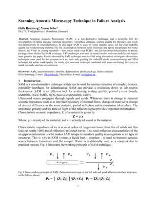
1. 1
Scanning Acoustic Microscopy Technique in Failure Analysis
Helle Rønsberga, Yavuz Kösea
DELTA, Venlighedsvej 4, Hoersholm, Denmark
Abstract. Scanning Acoustic Microscopy (SAM) is a non-destructive technique and a powerful tool for
investigation of plastic package moisture sensitivity, subsurface damages, coating quality for thickness and voids
non-destructively in microelectronics. In this paper SAM is used for some specific cases; (a) flip chip underfill
quality for voids/missing material fill, (b) Delamination between metal electrode and epoxy encapsulate for round
objects, (c) Voids in coating materials – here solder mask over PCBA and (d) intrusions/delamination in plastic
packages were studied by SAM technique. SAM technique was used in named studies with successfully and results
were given in the paper. Results obtained by SAM technique were verified using alternative techniques– destructive
techniques were used for this purpose such as; back side grinding for underfill voids, cross-sectioning and SEM
technique for solder mask quality for voids, dye penetrant technique combined with cross-sectioning for epoxy to
metal electrode interface delamination.
Keywords: SAM, microelectronics, obsolete, delamination, plastic package, failure analysis.
Helle Rønsberg, E-mail: HR@delta.dk, Yavuz Köse, E-mail: yak@delta.dk
1 Introduction
SAM is a non-destructive technique which can be used for internal structure of complex devices,
especially interfaces for delamination. SAM can provide a resolution down to sub-micron
thicknesses. SAM is an efficient tool for evaluating sealing quality, printed circuit boards,
underfills, BGA, SMDs, QFN, passive components, wafers.
Ultrasound waves propagate through liquids and solids. Whenever there is change in material
acoustic impedance such as at interface/boundary of internal flaws, change of material or change
of density difference in the same material, partial reflection and transmission takes place. The
amplitude, polarity and the time of flight of the reflected signal provides important information.
Characteristic acoustic impedance, Z, of a material is given by
Z = .v
Where, ρ = density of the material, and v = velocity of sound in the material.
Characteristic impedance of air is several orders of magnitude lower than that of solids and this
leads to nearly 100% (total reflection) reflected waves. This total reflection characteristics of the
air gaps/delamination is what makes SAM unique in interface quality investigations in all type of
structures. This is why in SAM system, a liquid bath – couplant – is used to transmit acoustic
waves between transducer and the sample. Water is traditionally used as a couplant due to
practical reasons. Fig. 1 illustrates the working principle of SAM technique.
Fig. 1 Basic working principle of SAM. Delamination/air gap on the left side and good adhesion interface structures
on the left are shown.
PR = │ (Z2-Z1) │/(Z2+Z1) PT = 2Z2/(Z2-Z1)
2. 2
Where PI = incident wave amplitude, PR = reflected wave amplitude and PT= transmitted wave
amplitude. As it can be seen from reflection formula, higher the characteristic impedance
difference means higher the reflection signal amplitude.
SAM is a non-destructive technique which uses ultrasound to examine surface and internal
structure of a solid material or structures e.g. an electrical component.
Schematic configuration of a scanning acoustic microscopy is shown in Figure 2, it composed of;
A piezoelectric transducer that sends pulses of acoustic waves through liquid couplant
and into the sample. Between pulses a receiver takes the echoes reflecting from sample.
In C-SAM transmitter and the receiver is the same piezoelectric transducer which
electronically switching between two modes of pulse sending and echo receiving.
Mechanical scanning unit which enables to focus the signals onto interest area and raster
scanning of the sample
Control unit or PC where the scanning and the data analysis are provided by the software
system.
Fig. 2: Schematic presentation of pulse-echo mode operated SAM instrumentation
There are two inspection modes; pulse-echo and through-transmission modes. Reflection signal
is used for pulse-echo mode imaging while transmitted signal is used for through-transmission
mode imaging.
Pulse-echo mode can determine and locate the delamination, defect and voids in bulk material
and provide high spatial resolution images. On the other hand, through-transmission images have
a less spatial resolution and cannot locate the defect position in bulk sample. Through-
transmission mode works as a complementary tool for pulse-echo mode findings and BGA
scanning.
Different modes of scanning options are available. Most used ones are;
A-Scan: A-Scan is real time waveform of reflected signals which is shown on XY-axis.
The horizontal scale (X-axis) defines the depth within a sample while the vertical scale
(Y-axis) defines amplitude and polarity of the reflected sound.
C-SAM: Classical SAM is primarily a reflection-based microscope that generates very
high-resolution images of a sample surface or a near surface plane but C-SAM
corresponds to bulk scan where internal investigation of beneath the sample surface is
conducted.
3. 3
B-Scan: B-Scan corresponds to imaginary cross-sectioning of the sample where the
sample is scanned cross-sectional.
Tomographic Acoustic Micrography Imaging (TAMITM
- SONIX): TAMI slices the bulk
material into micrometer thick layers and keeps the focus automatically at each layer.
TAMI enables to examine the whole sample by one scan in minutes.
Spatial resolution in SAM increases with increasing frequency but higher frequency means lover
depth information at the same time. The tradeoff between a low- and a high-frequency transducer
is in the depth of penetration and resolution.
The most important feature of SAM technique is that it is non-destructive & non-invasive.
Case stories
Having described the principles of the scanning acoustic microscope we will now present some
cases which are studied by SAM technique. Here four distinct cases which demonstrate how
SAM technique is practically and effectively detect the failures. Due to confidential nature of the
subjects in case stories, limited explanation was given about their details.
1 - Voids/missing underfill material in Flip Chip devices
Company A encounters short failures in their flip chip devices mounted on PCBA. Customer
believes that the voids/ missing underfill material between the solder balls result in short
connection during the reflow process. X-Ray technique was used for investigation. X-ray
detected existing short connections but not voids.
SAM technique was used for non-destructive analysis of the devices. SAM analysis was
conducted through the epoxy mold side. Due to the two sided and populated PCBA structure,
scanning through the substrate side was not effective enough. A demonstrative SAM micrograph
on a virgin sample is shown in Fig. 3. Rectangular white texture, between the solder balls in the
rows, shows missing underfill material.
Fig.3 SAM micrograph of an original sample. White rectangular texture between solder balls imply missing
underfill material.
In SAM analysis un-curved and plane surfaces helps for achieving best results by keeping the
surface at the focus and preventing diffraction of the signals during x-y plane raster scanning. In
case of here, Flip Chip devices, the surface was rough and curved. High frequencies, such as
100MHz and UHF (Ultra High Frequency) transducers were useless due to surface roughness
caused diffraction event.
For sharp images, destructively removal of the top epoxy mold was conducted by gentle
grinding. Exposing the flip chip device back side enabled high frequency transducer usage and
4. 4
better quality imaging. In Fig. 4, UHF transducer used TAMI mode SAM micrographs for a
sample is given. Images form a single scan thanks to TAMI mode scanning.
Fig. 4 UHF TAMI images for Flip Chip device. A) Die to underfill interface area, B) bulk of underfill, C) underfill
to substrate interface area.
In order to proof the accuracy of the SAM results, grinding from epoxy mold side down to
die/underfill interface were done by further grinding and then images were taken under
stereomicroscope. SAM image and corresponding stereo microscope image of the same device
were given in Fig 5. It is demonstrated that SAM could detect the underfill voids non-
destructively.
Fig. 5 On the right, optical micrograph of the Flip Chip device after removing epoxy mold and silicon die by
grinding, on the right SAM image of the same device before silicon die removal.
2 – Delamination study in round objects
Company B faces field-failed product returns. Reason for failure was attributed to delamination
between epoxy encapsulate and metal deposited ceramic electrode. Device has a round structure
and length of a couple of tens of millimeter, while having circumference around 10 mm.
Destructive analysis techniques, such as; cross-sectioning was used successfully for detection of
delamination but customer B wanted a non-destructive analysis option.
Even though SAM is conventionally used for flat surfaced-objects, usage for round object also is
getting spread out. A narrow scan line approximately 0.5 mm wide, along the device was
executed at several locations by turning the device using a 50 MHz transducer. Resulting SAM
micrograph is given in Fig.6. Device in image was expected to have partial delamination by
customer prior to SAM analysis in DELTA.
5. 5
Fig.6 SAM micrograph (A) of a partial delamination expected device with corresponding B-scan (cross-sectional
scan), Phase Gate mode image of corresponding scan micrograph (B) is shown.
As it can be seen from above Fig. 6, different modes of scanning possibilities were used and they
show consensus about the delaminated and the not-delaminated regions. It is important to
confirm the results with different mode of scanning in SAM, this enables the operator for correct
interpretation of the results before making the final conclusion.
In order to verify SAM results, dye penetrant test was used to highlight the delaminated areas
and observe visually. Devices were grinded in both ends until the border of the interest area.
Prior to grinding, devices were epoxy molded to prevent any artificially-induced failures during
grinding and handling. Resulting stereomicroscope image is given in Fig 7 for partially
delaminated device. Yellow line on the image shows the scan line along the device.
Fig.7 Optical micrograph of partially delamination expected device, yellow line shows a demonstrative scan line
along the device. Red are at the scan start shows the delaminated part of the interface in consensus with SAM results
given in Fig 6.
3 – Coating quality – voids in solder mask study
SAM technique is often used for coating quality studies such as for thickness of coating
measurement, intrusions of contaminants, delamination and trapped air bubbles/voids.
Customer C would like to investigate the quality of the solder mask for voids which works as
moisture trap and in longer term causes moisture related corrosion failures in PCBA assemblies.
In Fig 8, SAM micrograph is given with cross-sectional SEM (Scanning Electron Microscopy)
image of the same sample. SEM image was obtained after destructive cross-sectioning the
sample and observing in SEM. For the purpose of the analysis, SAM detected all voids in one
6. 6
scan for minutes. In the case of alternative, her SEM; cross-sectioning a random location, SEM
imaging for voids and then interpolating the result for all surface area. SAM provides this type
analysis – voids in coating – for transparent and opaque coatings non-destructively.
Fig.8 SAM micrograph of PCBA (A), and SEM image of cross-sectional analysis of PCBA (B). SAM shows total
void population in one scan in seconds. Alternatively SEM is used combined with cross-sectioning and interpolating
result to whole surface area of the PCBA.
4 – Counterfeit screening – Obsolete components
Due to rapid change in technology, components such as ICs are becoming outdated and their
production is being stopped. But due to marked needs for existing devices which uses those
outdated components, obsolete component market, so-called “grey-marked” emerges. Often re-
cycled, scrapped or counterfeit components are being refurbished, reworked and send into
marked illegally.
Company D uses obsolete components which were obtained from grey-marked. Components are
tested for functionality after procurement. Even though components passed functional tests,
customer demanded SAM analysis for device internal structures. SAM scanning details with
obtained results were given in Fig 9.
Fig.9 SAM micrographs for three obsolete SMDs. Device top and rear side SAM micrographs were given together,
Phase gate mode is used for highlighting delaminated interfaces for easy understanding of the scan results. Rear side
micrographs were provided after removal from PCBA.
7. 7
In Fig 9, component B has delamination in bond area, red colored bond areas therefore it is
critical and field failure in short time may occur. Evaluation of how critical an observed
delamination is carried out based on standards such as IPC/JEDEC J-STD-020D standard
“Moisture/Reflow Sensitivity Classification for Nonhermetic Solid State Surface Mount Devices
“ and DELTA’s
Conclusion
SAM is a non-destructive technique in failure analysis area and here is presented its versatile
usage for different purposes. Compared to alternative methods for same purposes, SAM is
practical and less time consuming. Here in this paper successful SAM analysis of different
subjects and failures were demonstrated for;
Missing underfill materials in Flip Chip ICs
Delamination between epoxy shell and metal electrode for round objects
Coating quality of solder mask for air bubbles – for transparent and opaque coatings
Counterfeit scanning for obsolete components
Compared to presented alternative test methods for the same purpose, SAM technique offers
non-destructive, practical, reliable and less time consuming option for users.
Acknowledgement
This article is issued under the project “Physics of Failure based reliable product development”
which is carried out by DELTA Denmark.