
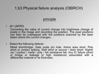
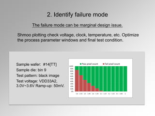
![Shmoo plotting check voltage, clock,
temperature, etc. Optimize the process
parameter windows and final test condition.
Sample wafer: #14[TT]
Test voltage: VDD33A2, 3.0V~3.6V Ramp-up: 50mV.
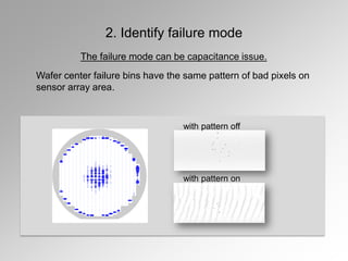
2. Identify failure mode
The failure mode can be marginal design issue.](https://image.slidesharecdn.com/icchipfailureanalyismethod-160525114309/85/Failure-Analysis-For-Integrated-Circuit-12-320.jpg)


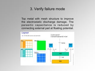

The document discusses failure analysis techniques in semiconductor IC development, emphasizing both electrical and physical analysis to improve yield before mass production. It details various methods such as X-ray, EMMI, and OBIRCH, alongside specific case studies highlighting failure modes and the importance of design and equipment performance. Additionally, it serves as training material for new workers, showcasing best practices and innovative approaches in failure analysis.


