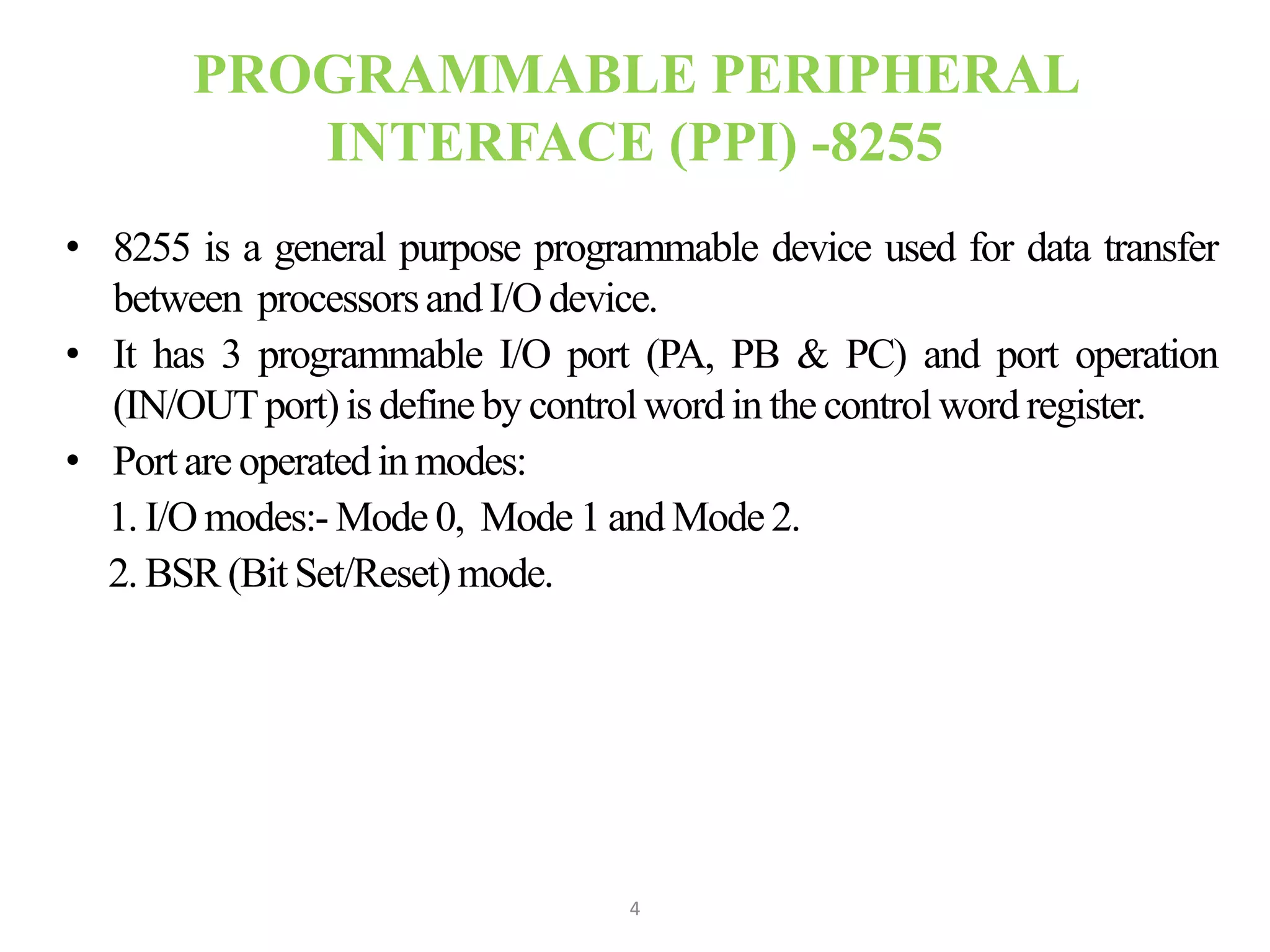
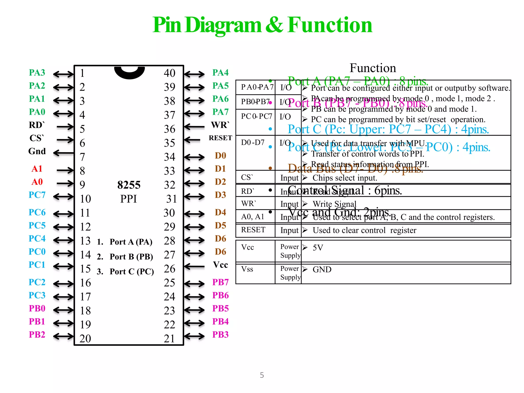
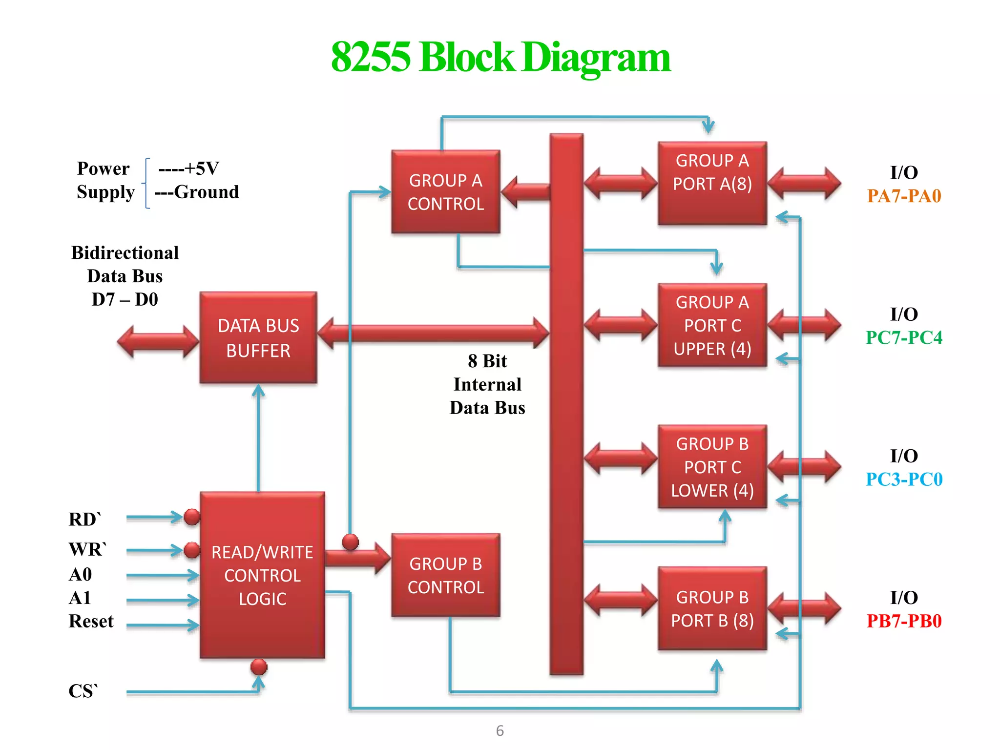
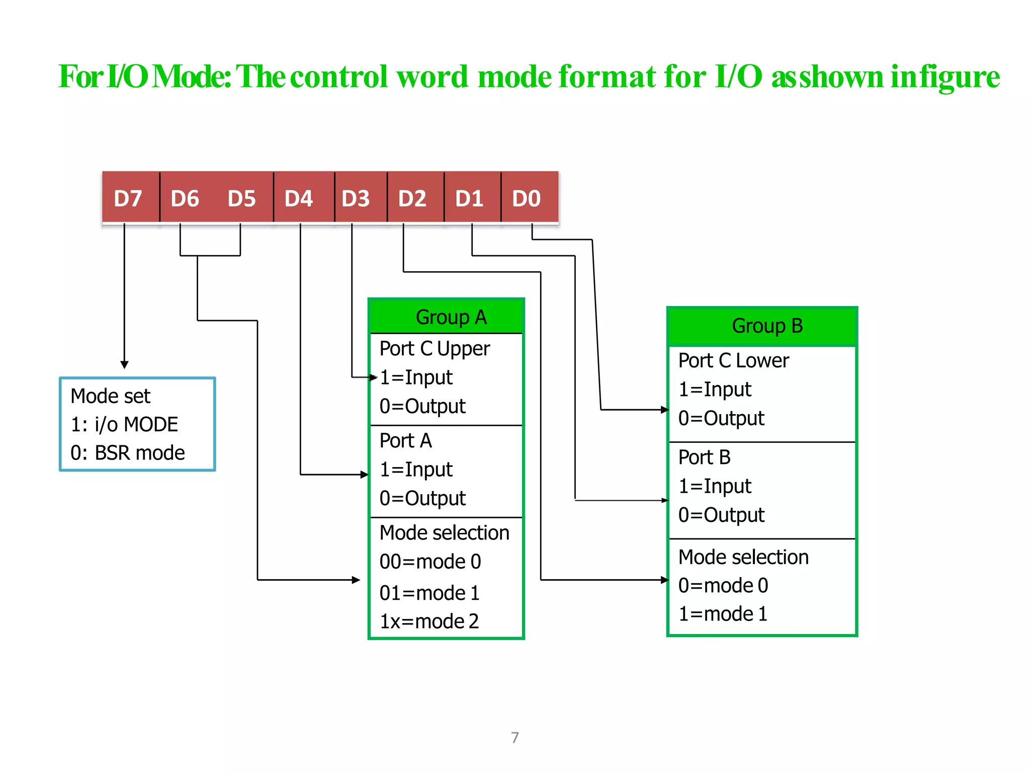
WELCOME
TO MY
PRESENTATION
Presented By
Km. Zahid parvez
Roll:10
Batch:9th
3rd Year 2nd semester.
PUNDRA UNIVERSITY OF SCIENCE &
TECHNOLOGY(PUST)
1
Presentation On
PROGRAMMABLE PERIPHERAL
INTERFACE (PPI) -8255
2
Presentation Outline
 Introduction of PPI.
 Pin Diagram & Function of PPI 8255.
 Block Diagram of PPI 8255.
 I/O Mode
3
PROGRAMMABLE PERIPHERAL
INTERFACE (PPI) -8255
• 8255 is a general purpose programmable device used for data transfer
between processorsand I/O device.
• It has 3 programmable I/O port (PA, PB & PC) and port operation
(IN/OUTport)is define by controlword in the controlword register.
• Port are operatedinmodes:
1. I/O modes:- Mode 0, Mode 1 and Mode2.
2. BSR (Bit Set/Reset)mode.
4
PinDiagram&Function
1 40
2 39
3 38
4 37
5 36
6 35
7 34
8 33
9 8255 32
10 PPI 31
11 30
12 29
13 28
14 27
15 26
16 25
17 24
18 23
19 22
20 21
PA3
PA2
PA1
PA0
PA4
PA5
PA6
PA7
D0
D1
D2
D3
D4
D5
D6
D6
PC7
PC6
PC5
PC4
PC0
PC1
PC2
PC3
PB0
PB1
PB2
PB7
PB6
PB5
PB4
PB3
Vcc
WR`
RESET
RD`
CS`
Gnd
A1
A0
1. Port A (PA)
2. Port B (PB)
3. Port C (PC)
• Port A (PA7 – PA0) : 8pins.
• Port B (PB7 - PB0) : 8pins.
• Port C (Pc: Upper: PC7 – PC4) : 4pins.
• Port C (Pc: Lower: PC3 – PC0) : 4pins.
• Data Bus (D7- D0) :8pins.
• Control Signal : 6pins.
• Vcc and Gnd: 2pins.
Function
PA0-PA7 I/O  Port can be configured either input or outputby software.
 PAcan be programmed by mode 0 , mode 1, mode 2 .
 PB can be programmed by mode 0 and mode 1.
 PC can be programmed by bit set/reset operation.
PB0-PB7 I/O
PC0-PC7 I/O
D0-D7 I/O  Used for data transfer withMPU.
 Transfer of control words toPPI.
 Read status information from PPI.
CS` Input  Chips select input.
RD` Input  Read signal.
WR` Input  Write Signal
A0, A1 Input  Used to select port A, B, C and the control registers.
RESET Input  Used to clear control register
Vcc Power
Supply
 5V
Vss Power
Supply
 GND
5
8255BlockDiagram
DATA BUS
BUFFER
READ/WRITE
CONTROL
LOGIC
GROUP A
CONTROL
GROUP B
CONTROL
GROUP A
PORT A(8)
GROUP A
PORT C
UPPER (4)
GROUP B
PORT C
LOWER (4)
GROUP B
PORT B (8)
Bidirectional
Data Bus
D7 – D0
Power ----+5V
Supply ---Ground
RD`
WR`
A0
A1
Reset
CS`
8 Bit
Internal
Data Bus
I/O
PA7-PA0
I/O
PC7-PC4
I/O
PC3-PC0
I/O
PB7-PB0
6
D7 D6 D5 D4 D3 D2 D1 D0
Group A
Port C Upper
1=Input
0=Output
Port A
1=Input
0=Output
Mode selection
00=mode 0
01=mode 1
1x=mode 2
Group B
Port C Lower
1=Input
0=Output
Port B
1=Input
0=Output
Mode selection
0=mode 0
1=mode 1
Mode set
1: i/o MODE
0: BSR mode
ForI/OMode:Thecontrol word mode format for I/O asshowninfigure
7
PROGRAMMABLE PERIPHERAL  INTERFACE (PPI) -8255

PROGRAMMABLE PERIPHERAL INTERFACE (PPI) -8255

  • 1.
    WELCOME TO MY PRESENTATION Presented By Km.Zahid parvez Roll:10 Batch:9th 3rd Year 2nd semester. PUNDRA UNIVERSITY OF SCIENCE & TECHNOLOGY(PUST) 1
  • 2.
  • 3.
    Presentation Outline  Introductionof PPI.  Pin Diagram & Function of PPI 8255.  Block Diagram of PPI 8255.  I/O Mode 3
  • 4.
    PROGRAMMABLE PERIPHERAL INTERFACE (PPI)-8255 • 8255 is a general purpose programmable device used for data transfer between processorsand I/O device. • It has 3 programmable I/O port (PA, PB & PC) and port operation (IN/OUTport)is define by controlword in the controlword register. • Port are operatedinmodes: 1. I/O modes:- Mode 0, Mode 1 and Mode2. 2. BSR (Bit Set/Reset)mode. 4
  • 5.
    PinDiagram&Function 1 40 2 39 338 4 37 5 36 6 35 7 34 8 33 9 8255 32 10 PPI 31 11 30 12 29 13 28 14 27 15 26 16 25 17 24 18 23 19 22 20 21 PA3 PA2 PA1 PA0 PA4 PA5 PA6 PA7 D0 D1 D2 D3 D4 D5 D6 D6 PC7 PC6 PC5 PC4 PC0 PC1 PC2 PC3 PB0 PB1 PB2 PB7 PB6 PB5 PB4 PB3 Vcc WR` RESET RD` CS` Gnd A1 A0 1. Port A (PA) 2. Port B (PB) 3. Port C (PC) • Port A (PA7 – PA0) : 8pins. • Port B (PB7 - PB0) : 8pins. • Port C (Pc: Upper: PC7 – PC4) : 4pins. • Port C (Pc: Lower: PC3 – PC0) : 4pins. • Data Bus (D7- D0) :8pins. • Control Signal : 6pins. • Vcc and Gnd: 2pins. Function PA0-PA7 I/O  Port can be configured either input or outputby software.  PAcan be programmed by mode 0 , mode 1, mode 2 .  PB can be programmed by mode 0 and mode 1.  PC can be programmed by bit set/reset operation. PB0-PB7 I/O PC0-PC7 I/O D0-D7 I/O  Used for data transfer withMPU.  Transfer of control words toPPI.  Read status information from PPI. CS` Input  Chips select input. RD` Input  Read signal. WR` Input  Write Signal A0, A1 Input  Used to select port A, B, C and the control registers. RESET Input  Used to clear control register Vcc Power Supply  5V Vss Power Supply  GND 5
  • 6.
    8255BlockDiagram DATA BUS BUFFER READ/WRITE CONTROL LOGIC GROUP A CONTROL GROUPB CONTROL GROUP A PORT A(8) GROUP A PORT C UPPER (4) GROUP B PORT C LOWER (4) GROUP B PORT B (8) Bidirectional Data Bus D7 – D0 Power ----+5V Supply ---Ground RD` WR` A0 A1 Reset CS` 8 Bit Internal Data Bus I/O PA7-PA0 I/O PC7-PC4 I/O PC3-PC0 I/O PB7-PB0 6
  • 7.
    D7 D6 D5D4 D3 D2 D1 D0 Group A Port C Upper 1=Input 0=Output Port A 1=Input 0=Output Mode selection 00=mode 0 01=mode 1 1x=mode 2 Group B Port C Lower 1=Input 0=Output Port B 1=Input 0=Output Mode selection 0=mode 0 1=mode 1 Mode set 1: i/o MODE 0: BSR mode ForI/OMode:Thecontrol word mode format for I/O asshowninfigure 7