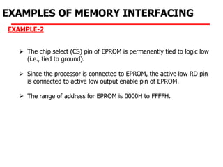
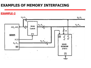
This document discusses memory interfacing with microprocessors. It describes three types of memory: process memory, primary/main memory, and secondary memory. It then provides details on typical EPROM and static RAM chips, including their pin configurations and control signals. Various memory decoders like 2-4 and 3-8 decoders are described. Examples are given to interface EPROM and RAM chips with an 8085 processor in systems with different memory capacities ranging from 8KB to 64KB. Diagrams show how the processor address lines are connected to the memory chips and how decoders are used to select individual memory chips.
The document discusses various topics related to 8085 microprocessor architecture including instruction cycle, memory, addressing modes, and programming model. It provides examples of interfacing EPROM and RAM memory chips with an 8085 processor using address decoding techniques. It also describes the five addressing modes used by the 8085 - direct, register, register indirect, immediate, and implicit addressing modes.
Interfacing involves connecting devices or programs to allow communication between a user and computer or between hardware and software. Memory interfacing specifically designs circuits that match a microprocessor's memory requirements by enabling it to read from and write to memory registers by generating appropriate signals. Address decoding is used to identify a specific memory register for a given address by decoding the microprocessor's address lines and generating a unique pulse for each possible address. This allows the microprocessor to select the appropriate memory chip, identify the register, and enable the correct buffer for reading or writing.
The document discusses interfacing memory chips with the 8085 microprocessor. It describes the basic concepts of memory interfacing such as address decoding, read and write timing diagrams, and interfacing circuits. It provides examples of interfacing a 2732 EPROM chip and an 8155 memory chip to the 8085 using address decoding logic and connecting control signal lines. Memory addressing ranges and internal structures are also covered.
The 8085 microprocessor has 64KB of addressable memory space that can be divided between RAM, EPROM, and I/O devices. Memory is typically divided with the first 8KB assigned to EPROM, the next 48KB to RAM, and the remaining address space allocated to I/O devices and left unused. I/O devices can be memory mapped, sharing the 64KB address space, or I/O mapped, using separate addresses from 00H to FFH and control signals to differentiate input and output.
A microprocessor is an electronic component that is used by a computer to do its work. It is a central processing unit on a single integrated circuit chip containing millions of very small components including transistors, resistors, and diodes that work together.
The 8085 microprocessor has 64KB of addressable memory space that can be allocated between RAM and EPROM based on the application's needs. The memory space can be divided into subsets including 8KB for EPROM, 48KB for RAM, 2KB for input/output devices, and the remaining 6KB unused. Memory mapping refers to how memory devices are assigned addresses within the 64KB memory space. The 8085 supports both memory-mapped I/O and I/O-mapped I/O for communicating with input/output devices.
The document discusses various topics related to microprocessors and computer architecture. It begins by providing details about the pins and functions of the 8085 microprocessor. It then discusses interfacing memory chips with the 8085 and provides an example. Next, it describes the block diagram and functions of the different units of the 8086 microprocessor. It also explains the different addressing modes used in 8086 with examples. The document then discusses the control word format for programming the I/O ports of the 8255 chip. In less than 3 sentences.
This document discusses different types of memory devices and interfaces. It describes ROM, EEPROM, SRAM, and DRAM memory types. It discusses address decoding and provides examples of memory interfaces for the 8088, 8086, 80386, and Pentium processors. The document also covers error detection techniques like parity checking, checksums, and cyclic redundancy checks (CRC). It provides an example of how Hamming codes can be used for error correction in memory.
This document provides an introduction to programmable logic devices including read-only memory (ROM) and programmable logic arrays (PLA). It discusses the basic components and operations of random-access memory (RAM) and ROM. It then describes how PLA and programmable array logic (PAL) work, using AND-OR logic to implement combinational logic functions. Examples are provided to demonstrate how to design circuits using these programmable logic devices and simplify Boolean functions for efficient implementation.
DIGITAL DESIGNS SLIDES 7 ENGINEERING 2ND YEARkasheen2803
This document provides information about computer memory. It discusses the different types of memory including internal memory (cache and primary memory) and external memory (magnetic disk, optical disk). It explains that memory is divided into cells that each have a unique address. It also describes the memory hierarchy from fastest and smallest capacity (cache) to slower and larger capacity (external storage). The document discusses different memory devices including RAM, ROM, DRAM and SRAM. It provides details on how memory works including addressing, read/write cycles, and decoding. It also covers programmable logic devices like PLDs, PALs, PLAs, CPLDs and FPGAs.
The document discusses different types of computer memory, including ROM, RAM, SRAM, and DRAM. It describes how memory devices work and how they are connected to microprocessors. Specific examples of interfacing 8088, 80188, and 80386 microprocessors to EPROM, RAM, and flash memory are provided through diagrams and explanations of address decoding and control signal usage. Error detection techniques like parity checking are also summarized.
The document discusses memory mapping and interfacing memory with the 8085 microprocessor. It describes two methods of memory address decoding:
1) Absolute address decoding - Each memory location has a unique address. Extra decoders are needed but allow easy expansion.
2) Linear select decoding - Simplifies decoding circuits but wastes memory space and makes expansion difficult as multiple addresses map to each location.
The document provides examples of implementing both methods using 8085 with 8KB memory blocks, and discusses advantages and disadvantages of each approach. Diagrams illustrate the memory maps and interfacing circuitry.
This document discusses microprocessor architecture and memory interfacing. It provides an overview of the basic parts and operations of a microprocessor-based system including the CPU, memory, and I/O devices. It describes the different types of buses (address bus, data bus, control bus) and how they transfer data and signals. It also explains memory interfacing and addressing, different types of memory (RAM, ROM), and how microprocessors access memory using an address bus.
Chp3 designing bus system, memory & io copymkazree
The document discusses various concepts related to designing bus systems and interfacing memory and I/O devices with the Motorola 68000 microprocessor. It covers the address and data buses of the 68000, addressing modes, designing memory decoders, generating acknowledge signals, direct memory access, and memory-mapped I/O using devices like the 6821 PIA and 6850 ACIA.
The document discusses timing diagrams and machine cycles in the 8085 microprocessor. It provides details on the different machine cycles - opcode fetch, memory read, memory write, I/O read, and I/O write. It explains that the 8085 has a clock signal divided into T-states that represent portions of machine cycle operations. Examples are given of timing diagrams for instructions like MOV B,C, MVI B,43, and STA 526A to illustrate the sequence of events over multiple T-states.
The 8051 microcontroller has the following key features:
- 4K bytes of ROM, 128 bytes of RAM, four 8-bit I/O ports, and two 16-bit timers. It has pins for serial communication and can address up to 64K bytes each of external code and data memory. The 40-pin device uses 32 pins for I/O, with some pins having dual purposes. It uses a crystal oscillator connected to pins 18 and 19 to generate the clock signal. The 8051 has separate internal memory spaces for code and data and can access additional external memory. Special function registers like the Program Status Word and Accumulator control various functions.
A microprocessor is an electronic component that is used by a computer to do its work. It is a central processing unit on a single integrated circuit chip containing millions of very small components including transistors, resistors, and diodes that work together. Some microprocessors in the 20th century required several chips. Microprocessors help to do everything from controlling elevators to searching the Web. Everything a computer does is described by instructions of computer programs, and microprocessors carry out these instructions many millions of times a second. [1]
Microprocessors were invented in the 1970s for use in embedded systems. The majority are still used that way, in such things as mobile phones, cars, military weapons, and home appliances. Some microprocessors are microcontrollers, so small and inexpensive that they are used to control very simple products like flashlights and greeting cards that play music when you open them. A few especially powerful microprocessors are used in personal computers.
The document discusses the history and evolution of microprocessors from early 4-bit processors of the 1970s to modern 64-bit processors. It covers early technologies like PMOS and NMOS and describes processors like the Intel 4004, 8008, 8080, and 8085. It also discusses the internal architecture of processors like the 8085 including components like the ALU, registers, program counter, and memory interfacing. Modern processors including the Pentium series and RISC processors are also briefly outlined.
This document discusses memory and I/O interfacing with microprocessors. It begins by defining an interface as the point of interaction between components, allowing independent functioning through input/output systems. It then provides examples of addressing schemes like multiplexing address and data lines, and decoding techniques like exhaustive and partial decoding. Finally, it covers interfacing various memory chips like RAM, ROM and interfacing I/O devices through parallel and serial communication.
This document discusses memory and I/O interfacing with the 8085 microprocessor. It defines interfaces as points of interaction between components that allow communication. Memory interfacing requires address decoding and multiplexing of address and data lines. I/O devices can be interfaced either through memory mapping or I/O mapping. Common memory types include RAM, ROM, SRAM and DRAM. RAM can be static or dynamic. ROM includes PROM, EPROM and EEPROM. A stack is a reserved part of memory used to temporarily store information during program execution.
A microprocessor is a programmable logic device that accepts binary instructions from memory, processes data according to those instructions, and provides results as output. The 8085 microprocessor has a power supply of +5V and clock frequency of 3MHz. It can perform operations like arithmetic, logical operations, and store data temporarily in memory locations called the stack. An instruction is a binary pattern that commands the microprocessor to perform a specific function.
Interfacing memory with 8086 microprocessorVikas Gupta
This document discusses interfacing memory with the 8086 microprocessor. It begins by defining different types of memory like RAM, ROM, EPROM, and EEPROM. It then discusses memory fundamentals like capacity, organization, and standard memory ICs. The document explains two methods of address decoding - absolute and partial decoding. It provides examples of interfacing 32KB RAM, 32K words of memory, and a combination of ROM, EPROM, and RAM with the 8086 using address decoding techniques. Diagrams and tables are included to illustrate the memory mapping and generation of chip select logic.
The document discusses microprocessors and the 8085 microprocessor. It provides details on:
1) The internal architecture and components of microprocessors and the 8085 microprocessor.
2) The different types of operations microprocessors can perform including internal data operations, microprocessor initiated operations, and peripheral initiated operations.
3) The addressing modes, instruction set, registers, and instruction types/formats of the 8085 microprocessor.
Similar to interfacing1 lecture notes for eng 5.ppt (20)
- Arrays allow storing multiple values of the same type sequentially in memory. They have a fixed size or dimension.
- To declare an integer array of size 4, we write "int arr[4]". Individual elements can be accessed using indexes from 0 to dimension-1.
- Strings in C++ are arrays of characters that end with a null character. Common string functions like strcpy(), strcat(), strlen() allow manipulating strings.
NEW TRAINING ON E-RESOURCES ACCESS AND USE.pptJumanneChiyanda
This document provides information about a training on accessing and using electronic resources offered by the Directorate of Library Services at MBEYA University of Science and Technology. It introduces the university's Dr. Magufuli Library and its resources. It then describes the various categories of electronic resources available, how to access them through search techniques and popular web browsers, and how they can be used for research, teaching, and student assignments. The document concludes by providing hands-on practice with several electronic resource platforms, databases, and search engines through assigned usernames and passwords.
Applications of artificial Intelligence in Mechanical Engineering.pdfAtif Razi
Historically, mechanical engineering has relied heavily on human expertise and empirical methods to solve complex problems. With the introduction of computer-aided design (CAD) and finite element analysis (FEA), the field took its first steps towards digitization. These tools allowed engineers to simulate and analyze mechanical systems with greater accuracy and efficiency. However, the sheer volume of data generated by modern engineering systems and the increasing complexity of these systems have necessitated more advanced analytical tools, paving the way for AI.
AI offers the capability to process vast amounts of data, identify patterns, and make predictions with a level of speed and accuracy unattainable by traditional methods. This has profound implications for mechanical engineering, enabling more efficient design processes, predictive maintenance strategies, and optimized manufacturing operations. AI-driven tools can learn from historical data, adapt to new information, and continuously improve their performance, making them invaluable in tackling the multifaceted challenges of modern mechanical engineering.
Impartiality as per ISO /IEC 17025:2017 StandardMuhammadJazib15
This document provides basic guidelines for imparitallity requirement of ISO 17025. It defines in detial how it is met and wiudhwdih jdhsjdhwudjwkdbjwkdddddddddddkkkkkkkkkkkkkkkkkkkkkkkwwwwwwwwwwwwwwwwwwwwwwwwwwwwwwwwwwwwwwwwwwwwwwwwwwwwwwwwwwwwwwwwwwwwwwwwwwwwwwwwwwwwwwwwwwwwwwwwwwwwwwwwwwwwwwwwwwwwwwwwwwwwwwwwwwwwwwwwwwwwwwwwwwwwwwwwwioiiiiiiiiiiiii uwwwwwwwwwwwwwwwwhe wiqqqqqqqqqqqqqqqqqqqqqqqqqqqqqqqqqqqqqqqqqqqqqqqqqqqqqqqqqqqqqqqqqqqqqqqqqqqqqqqqqqqqqqqqqqqqqqqqqqqqqqqqqqqqqqqqqqqqqqqqqqqqqqqqqqqqqqqqqqqqqqqqqqqqqqqqqqqqqqqqqqqqqqqqqqqqqqqqqqqqqqqqqqqqqqqqqqq gbbbbbbbbbbbbb owdjjjjjjjjjjjjjjjjjjjj widhi owqqqqqqqqqqqqqqqqqqqqqqqqqqqqqqqqqq uwdhhhhhhhhhhhhhhhhhhhhhhhhhhhhhhhhhhhhhhhhhhhhhhhhhhhhhhhhhhhhhhhhhhhhhhhhhhhhhhhhhhhhhhhhhhhhhhhhhhhhhhhhhhhhhhhhhhhhhhhhhhhhhhhhhhhhhhhhhhhhhhhhhhhhhhhhhhhhhhhhhhhhhhwqiiiiiiiiiiiiiiiiiiiiiiiiiiiiw0pooooojjjjjjjjjjjjjjjjjjjjjjjjjjjjjjjjjjjjjjjjjjjjjjjjjjjjjj whhhhhhhhhhh wheeeeeeee wihieiiiiii wihe
e qqqqqqqqqqeuwiiiiiiiiiiiiiiiiiiiiiiiiiiiiiiiiiiiiiiiiiiiiiiiiiiiiiiiiiiiiiiiiiiiiiiiiiiiiiiiiiiiiiiiiiiiiiiiiiiiiiiiiiiiiiiiiiiiiiiiiiiiiiiiiiiiiiiiiiiiiiiiiiiiiiiiiiiiiiiiiiiiiiiiiiiiiiiiiiiiiiiiiiiiiiiiiiiiiiiiiiiiiiiiiiiiiiiiiiiiiiiiiiiiiiiiiiiiiiiiiiiiiiiiiiiiiiiiiiiiiiiiiiiiiiiiiiiiiiiiiiiiiiiiiiiiiiiiiiiiiiiiiiiiiiiiiiqw dddddddddd cccccccccccccccv s w c r
cdf cb bicbsad ishd d qwkbdwiur e wetwwwwwwwwwwwwwwwwwwwwwwwwwwwwwwwwwwwwwwwwwwwwwwwwwwwwwwwwwwwwwwwwwwwwww w
dddddddddddddddddddddddddddddddddddddddddddddddddddddddddddddddddddddddddddddddddddddddddddddddddddddddddddfffffffffffffffffffffffffffffffffffffffffffffffffffffffffffffffffffffffffffffffffffffffffffffffffffffffffffffffffffffffffffffffffffffffffffffffffffffffffffffffffffffffffffffffffffffffffffffffffffffffffffffffffffffw
uuuuhhhhhhhhhhhhhhhhhhhhhhhhe qiiiiiiiiiiiiiiiiiiiiiiiiiiiiiiiiiiiiiiiiiiiiiiiiiiiiiiiiiiiiiii iqqqqqqqqqqqqqqqqqqqqqqqqqqqqqqqqqqqqqqqqqqqqqqqqqqqqqqqqqqqqqqqqqqqqqqqqqqqqqqqqqqqqqqqqqqqqqqqqqqqqqqqqqqqqqqqqqqqqqqqqqqqqqqqqqqqqq eeeeeeeeeeeeeeeeeeeeeeeeeeeeeeeeeeeeeeeeeeeeeeeeeeeeeeeeeeeeeeeeeeeeeeeeeeeeeeeeeeeeeeeeeeeeeeeeee qqqqqqqqqqqqqqqqqqqqqqqqqqqqqqqqqqqqqqqqqqqqqqqqqqqqqqqqqqqqqqqqqqqqqqqqqqqqqqqqqqqqqqqqqqqqqqqqqqqqqqqqqqqqqqccccccccccccccccccccccccccccccccccccccccccccccccccccccccccccc ccccccccccccccccccccccccccccccccccc bbbbbbbbbbbbbbbbbbbbbbbbbbbbbbbbbbbbbbbbbbbbbbbbbbbbbbbbbbbbbbbbbbbbbbbbbbbbbbbbu uuuuuuuuuuuuuuuuuuuuuuuuuuuuuuuuuuuuuuuuuuuuuuuuuuuuuuuuuuuuuuuuuuuuuuuuuuuuuuuuuuuuuuuuuuuuuuuuuuuuuuuuuuuuuuuuuuuuuuuuuuuuuuuuuuuuuuuuuuuuuuuuuuuuuuuuuum
m
m mmmmmmmmmmmmmmmmmmmmmmmmmmmmmmmmmmmmmmmmmmmmmmmmmmmmmmmmmmmmmmmmmmmmmmmmmmmmmmmmmmmmmmmmmmmm m i
g i dijsd sjdnsjd ndjajsdnnsa adjdnawddddddddddddd uw
Prediction of Electrical Energy Efficiency Using Information on Consumer's Ac...PriyankaKilaniya
Energy efficiency has been important since the latter part of the last century. The main object of this survey is to determine the energy efficiency knowledge among consumers. Two separate districts in Bangladesh are selected to conduct the survey on households and showrooms about the energy and seller also. The survey uses the data to find some regression equations from which it is easy to predict energy efficiency knowledge. The data is analyzed and calculated based on five important criteria. The initial target was to find some factors that help predict a person's energy efficiency knowledge. From the survey, it is found that the energy efficiency awareness among the people of our country is very low. Relationships between household energy use behaviors are estimated using a unique dataset of about 40 households and 20 showrooms in Bangladesh's Chapainawabganj and Bagerhat districts. Knowledge of energy consumption and energy efficiency technology options is found to be associated with household use of energy conservation practices. Household characteristics also influence household energy use behavior. Younger household cohorts are more likely to adopt energy-efficient technologies and energy conservation practices and place primary importance on energy saving for environmental reasons. Education also influences attitudes toward energy conservation in Bangladesh. Low-education households indicate they primarily save electricity for the environment while high-education households indicate they are motivated by environmental concerns.
Build the Next Generation of Apps with the Einstein 1 Platform.
Rejoignez Philippe Ozil pour une session de workshops qui vous guidera à travers les détails de la plateforme Einstein 1, l'importance des données pour la création d'applications d'intelligence artificielle et les différents outils et technologies que Salesforce propose pour vous apporter tous les bénéfices de l'IA.
Sri Guru Hargobind Ji - Bandi Chor Guru.pdfBalvir Singh
Sri Guru Hargobind Ji (19 June 1595 - 3 March 1644) is revered as the Sixth Nanak.
• On 25 May 1606 Guru Arjan nominated his son Sri Hargobind Ji as his successor. Shortly
afterwards, Guru Arjan was arrested, tortured and killed by order of the Mogul Emperor
Jahangir.
• Guru Hargobind's succession ceremony took place on 24 June 1606. He was barely
eleven years old when he became 6th Guru.
• As ordered by Guru Arjan Dev Ji, he put on two swords, one indicated his spiritual
authority (PIRI) and the other, his temporal authority (MIRI). He thus for the first time
initiated military tradition in the Sikh faith to resist religious persecution, protect
people’s freedom and independence to practice religion by choice. He transformed
Sikhs to be Saints and Soldier.
• He had a long tenure as Guru, lasting 37 years, 9 months and 3 days
An In-Depth Exploration of Natural Language Processing: Evolution, Applicatio...DharmaBanothu
Natural language processing (NLP) has
recently garnered significant interest for the
computational representation and analysis of human
language. Its applications span multiple domains such
as machine translation, email spam detection,
information extraction, summarization, healthcare,
and question answering. This paper first delineates
four phases by examining various levels of NLP and
components of Natural Language Generation,
followed by a review of the history and progression of
NLP. Subsequently, we delve into the current state of
the art by presenting diverse NLP applications,
contemporary trends, and challenges. Finally, we
discuss some available datasets, models, and
evaluation metrics in NLP.
Supermarket Management System Project Report.pdfKamal Acharya
Supermarket management is a stand-alone J2EE using Eclipse Juno program.
This project contains all the necessary required information about maintaining
the supermarket billing system.
The core idea of this project to minimize the paper work and centralize the
data. Here all the communication is taken in secure manner. That is, in this
application the information will be stored in client itself. For further security the
data base is stored in the back-end oracle and so no intruders can access it.
Sachpazis_Consolidation Settlement Calculation Program-The Python Code and th...Dr.Costas Sachpazis
Consolidation Settlement Calculation Program-The Python Code
By Professor Dr. Costas Sachpazis, Civil Engineer & Geologist
This program calculates the consolidation settlement for a foundation based on soil layer properties and foundation data. It allows users to input multiple soil layers and foundation characteristics to determine the total settlement.
2. Programs and data that are executed by the
microprocessor have to be stored in ROM/EPROM and RAM
8085 has 16 address lines (A0 - A15)
Maximum of 64 KB (= 2^16 bytes) of memory locations
can be interfaced
Memory address space takes values from 0000H to FFFFH
IO/M , RD and WR when it wants to read from and write
into memory or I/O devices
INTERFACING MEMORY WITH 8085
3. CE or CS(chip enable or chip select)
OE or RD (output enable or read)
WE or WR (write enable or write)
INTERFACING MEMORY (memory pins)WITH 8085
4. Generation of Control Signals for Memory
8085 activates IO/M , RD and WR signals as shown
in the Table
INTERFACING MEMORY WITH 8085
5. Using IO/M , RD and WR two control signals
MEMR(memory read) and MEMW(memory write)
INTERFACING MEMORY WITH 8085
6. Specification of IC 2764:
8 KB (8 x 2^10 byte) EPROM chip
13 address lines (2^13 bytes = 8 KB)
Address range allocated to the chip is
0000H – 1FFFH
INTERFACE AN IC 2764 WITH 8085
7. 13 address lines of IC are connected to A0-A12
Remaining (A13, A14, A15) are connected to
address decoder formed using logic gates
Output of decoder is connected to the CE pin of IC
Chip is enabled whenever the 8085 places an
address allocated to EPROM chip in the address
bus
INTERFACE AN IC 2764 WITH 8085
10. EXAMPLES OF MEMORY INTERFACING
EXAMPLE-2
Consider a system in which the full memory space 64KB is utilized for
EPROM memory. Interface the EPROM with 8085 processor.
The memory capacity is 64 Kbytes. i.e. 2^n = 64 x 1024 bytes
where n = address lines. So, n = 16.
In this system the entire 16 address lines of the processor are
connected to address input pins of memory IC in order to address
the internal locations of memory.
11. EXAMPLES OF MEMORY INTERFACING
EXAMPLE-2
The chip select (CS) pin of EPROM is permanently tied to logic low
(i.e., tied to ground).
Since the processor is connected to EPROM, the active low RD pin
is connected to active low output enable pin of EPROM.
The range of address for EPROM is 0000H to FFFFH.
13. EXAMPLES OF MEMORY INTERFACING
EXAMPLE-3
Consider a system in which the available 64KB memory space is equally
divided between EPROM and RAM. Interface the EPROM and RAM with
8085 processor.
Implement 32KB memory capacity of EPROM using single IC 27256.
32KB RAM capacity is implemented using single IC 62256.
The 32KB memory requires 15 address lines and so the address lines
A0 - A14 of the processor are connected to 15 address pins of both
EPROM and RAM.
14. EXAMPLES OF MEMORY INTERFACING
EXAMPLE-3
The unused address line A15 is used as to chip select. If A15 is 1, it select
RAM and If A15 is 0, it select EPROM.
Inverter is used for selecting the memory.
The memory used is both Ram and EPROM, so the low RD and WR pins of
processor are connected to low WE and OE pins of memory respectively.
The address range of EPROM will be 0000H to 7FFFH and that of RAM will
be 8000H to FFFFH.
16. EXAMPLES OF MEMORY INTERFACING
EXAMPLE-4
Consider a system in which 32KB memory space is implemented using
four numbers of 8KB memory. Interface the EPROM and RAM with 8085
processor.
The total memory capacity is 32KB. So, let two number of 8KB
memory be EPROM and the remaining two numbers be RAM.
Each 8KB memory requires 13 address lines and so the address lines
A0- A12 of the processor are connected to 13 address pins of all the
memory.
17. EXAMPLES OF MEMORY INTERFACING
EXAMPLE-4
The address lines and A13 - A14 can be decoded using a 2-to-4
decoder to generate four chip select signals.
These four chip select signals can be used to select one of the four
memory IC at any one time.
The address line A15 is used as enable for decoder.
The simplified schematic memory organization is shown.