Download to read offline

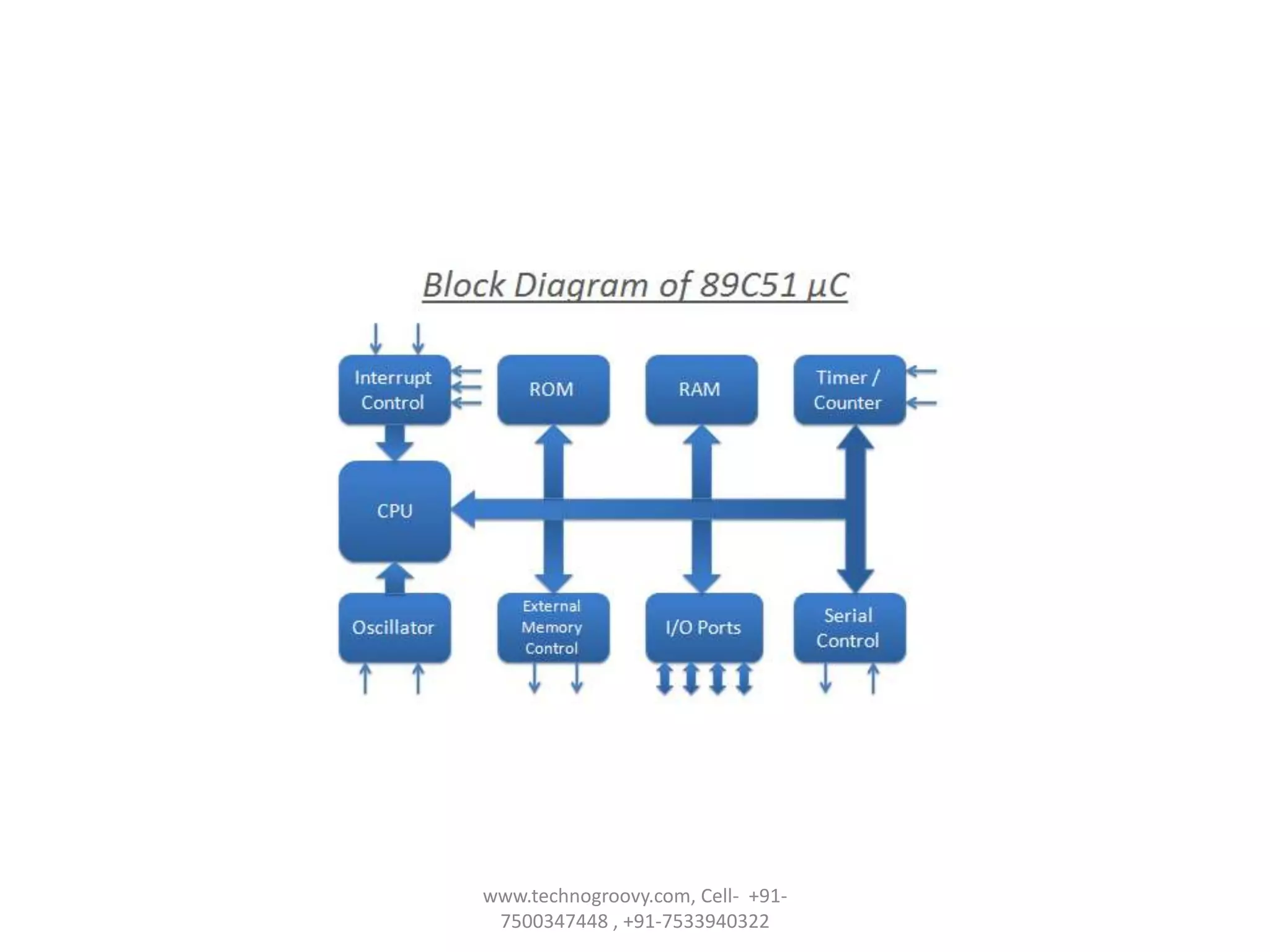
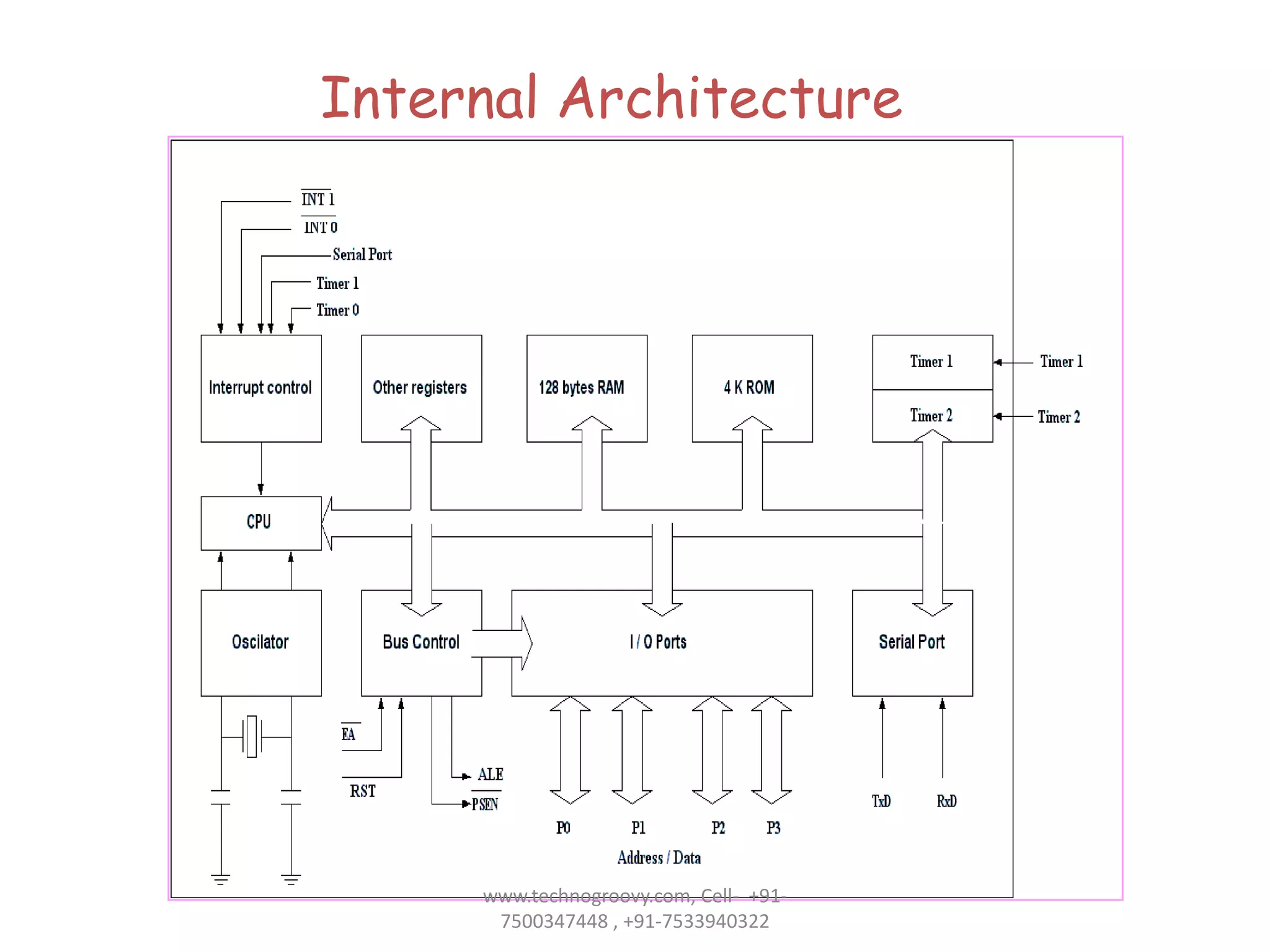
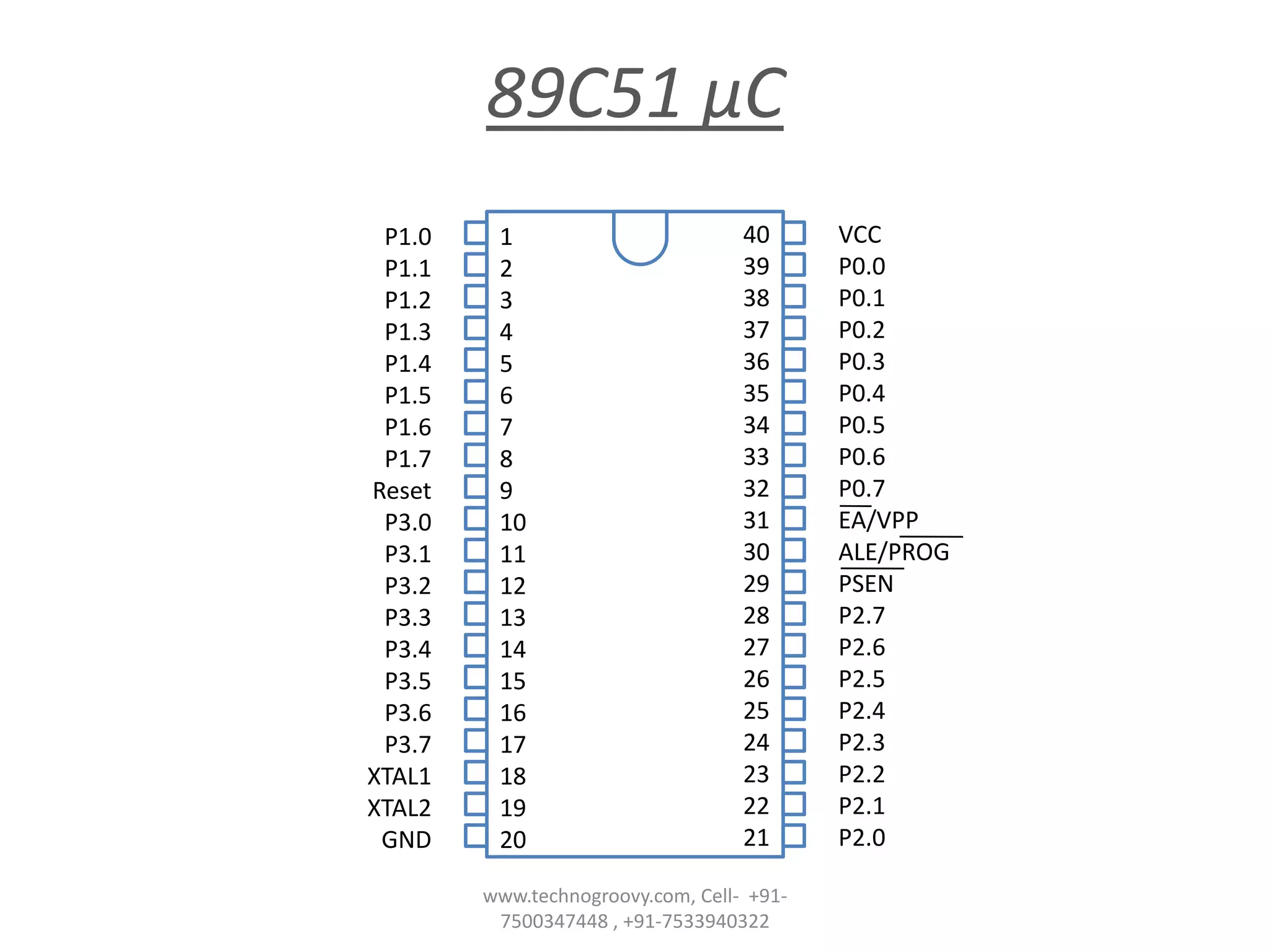
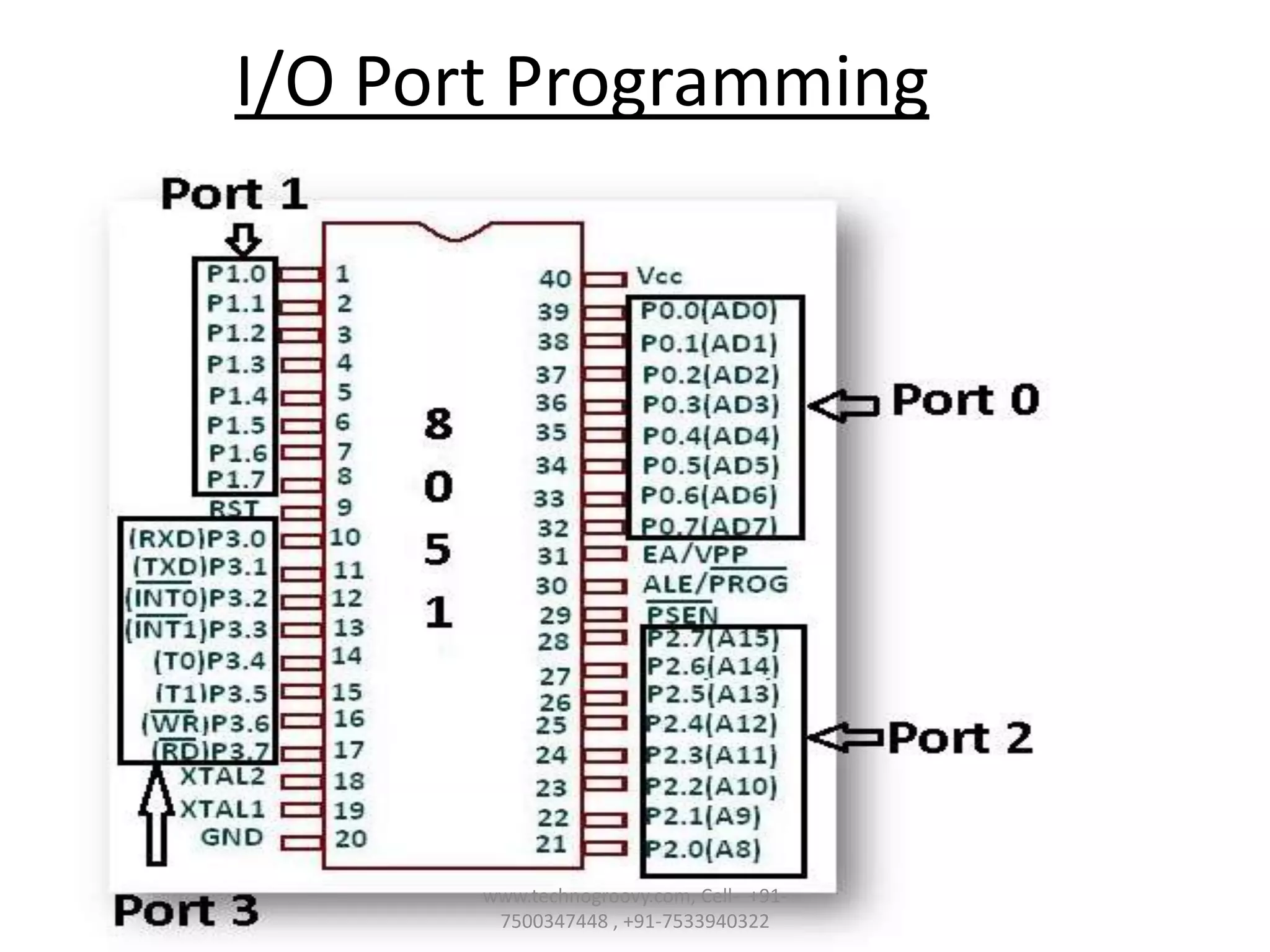


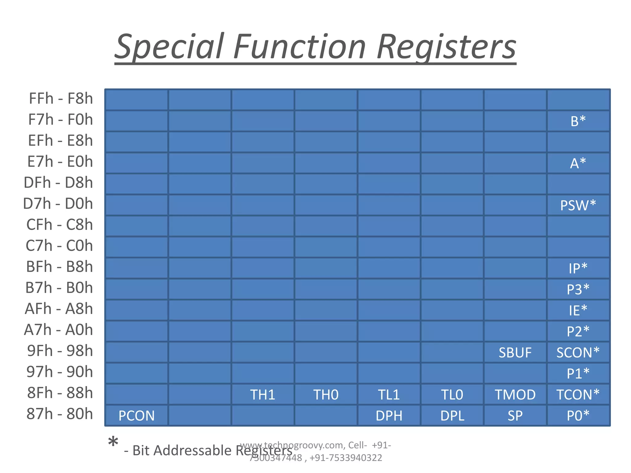
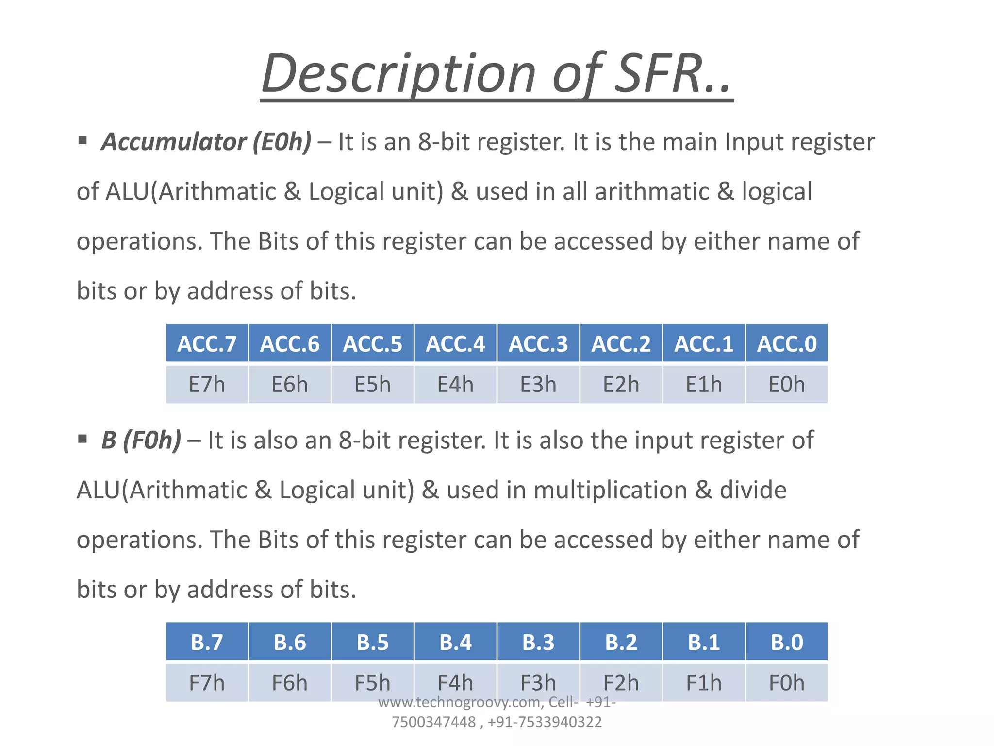
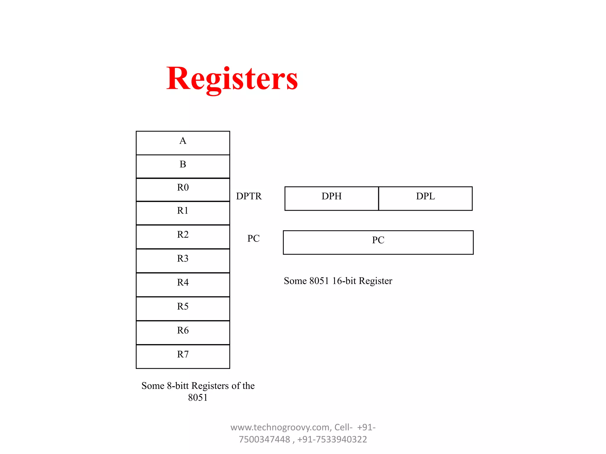
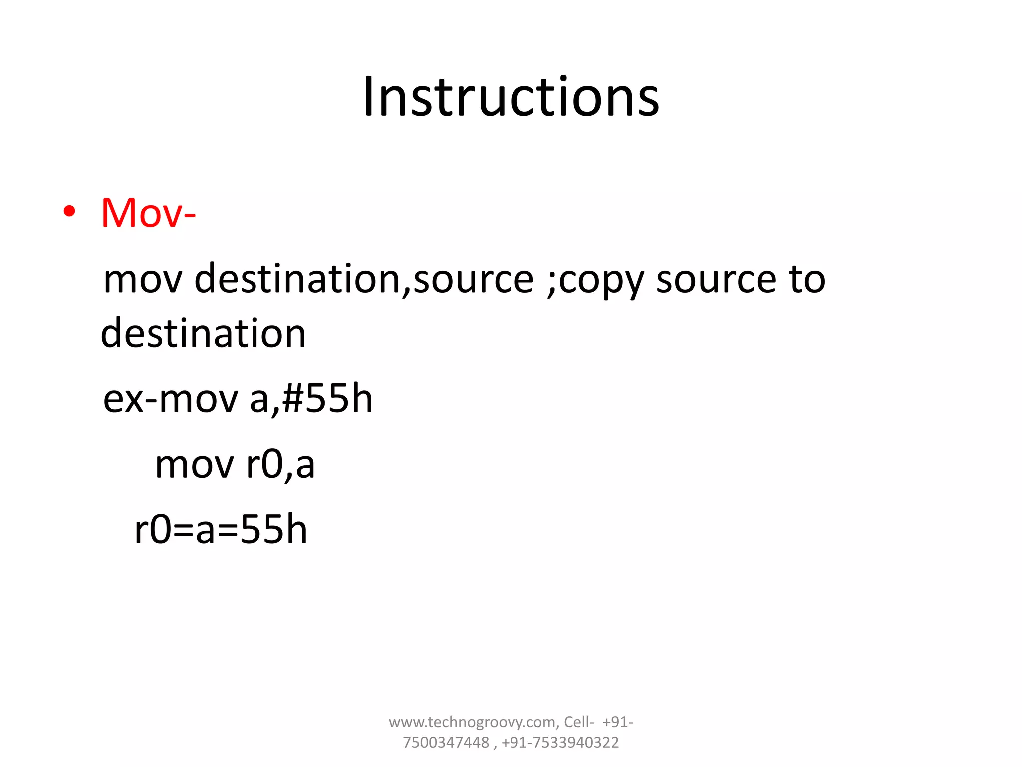


The document provides detailed information about the AT89C51 microcontroller, including its pinout configurations, port functionalities, and special function registers (SFRs). It explains the purpose of various pins, such as input/output ports and their alternate functions, along with activation methods for resets and external memory access. Additionally, it outlines instruction examples for programming the microcontroller and provides contact information for Technogroovy Systems India Pvt Ltd.