⚫An example forCISC Processor
.
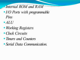
⚫Harvard Architecture
⚫Collection of 8 and 16 bit registers
and 8 bit memory locations.
⚫External Memory can be interfaced.
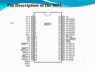
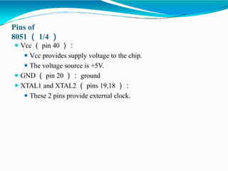
Pins of
8051 (1/4 )
⚫ Vcc ( pin 40 ):
⚫ Vcc provides supply voltage to the chip.
⚫ The voltage source is +5V.
⚫ GND ( pin 20 ): ground
⚫ XTAL1 and XTAL2 ( pins 19,18 ):
⚫ These 2 pins provide external clock.
6.
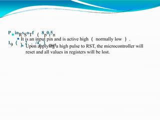
P⚫inRsSoTf ( 8p0i5n
19() 2 : /4r ) eset
⚫ It is an input pin and is active high ( normally low ) .
⚫ Upon applying a high pulse to RST, the microcontroller will
reset and all values in registers will be lost.
7.
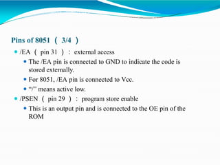
Pins of 8051( 3/4 )
⚫ /EA ( pin 31 ): external access
⚫ The /EA pin is connected to GND to indicate the code is
stored externally.
⚫ For 8051, /EA pin is connected to Vcc.
⚫ “/” means active low.
⚫ /PSEN ( pin 29 ): program store enable
⚫ This is an output pin and is connected to the OE pin of the
ROM
8.
Pins of 8051( 4/4 )
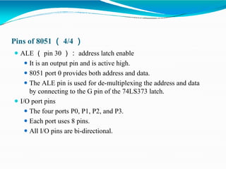
⚫ ALE ( pin 30 ): address latch enable
⚫ It is an output pin and is active high.
⚫ 8051 port 0 provides both address and data.
⚫ The ALE pin is used for de-multiplexing the address and data
by connecting to the G pin of the 74LS373 latch.
⚫ I/O port pins
⚫ The four ports P0, P1, P2, and P3.
⚫ Each port uses 8 pins.
⚫ All I/O pins are bi-directional.
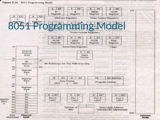
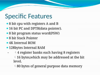
Specific Features
⚫8 bitcpu with registers A and B
⚫16 bit PC and DPTR(data pointer).
⚫8 bit program status word(PSW)
⚫8 bit Stack Pointer
⚫4K Internal ROM
⚫128bytes Internal RAM
- 4 register banks each having 8 registers
16 bytes,which may be addressed at the bit
level.
80 bytes of general purpose data memory
13.
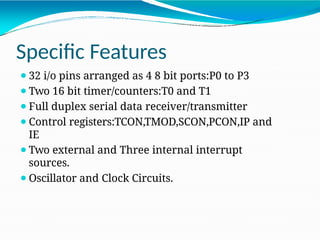
Specific Features
⚫32 i/opins arranged as 4 8 bit ports:P0 to P3
⚫Two 16 bit timer/counters:T0 and T1
⚫Full duplex serial data receiver/transmitter
⚫Control registers:TCON,TMOD,SCON,PCON,IP and
IE
⚫Two external and Three internal interrupt
sources.
⚫Oscillator and Clock Circuits.
14.
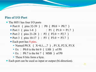
Pins of I/OPort
⚫ The 8051 has four I/O ports
⚫ Port 0 ( pins 32-39 ): P0 ( P0.0 ~ P0.7 )
⚫ Port 1 ( pins 1-8 ) : P1 ( P1.0 ~ P1.7 )
⚫ Port 2 ( pins 21-28 ): P2 ( P2.0 ~ P2.7 )
⚫ Port 3 ( pins 10-17 ): P3 ( P3.0 ~ P3.7 )
⚫ Each port has 8 pins.
⚫ Named P0.X ( X=0,1,...,7 ) , P1.X, P2.X, P3.X
⚫ Ex : P0.0 is the bit 0 ( LSB ) of P0
⚫ Ex : P0.7 is the bit 7 ( MSB ) of P0
⚫ These 8 bits form a byte.
⚫ Each port can be used as input or output (bi-direction).
15.
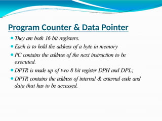
Program Counter &Data Pointer
⚫They are both 16 bit registers.
⚫Each is to hold the address of a byte in memory
⚫PC contains the address of the next instruction to be
executed.
⚫DPTR is made up of two 8 bit register DPH and DPL;
⚫DPTR contains the address of internal & external code and
data that has to be accessed.
16.
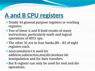
A and BCPU registers
⚫Totally 34 general purpose registers or working
registers.
⚫Two of these A and B hold results of many
instructions, particularly math and logical
operations of 8051 cpu.
⚫The other 32 are in four banks,B0 – B3 of eight
registers each.
⚫A(accumulator) is used for
addition,subtraction,mul,div,boolean bit
manipulation and for data transfers.
⚫But B register can only be used for mul and div
operations.
17.
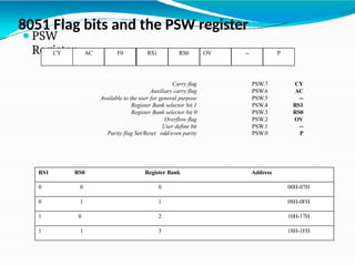
8051 Flag bitsand the PSW register
⚫PSW
Register
CY AC F0 RS1 RS0 OV -- P
Carry flag PSW.7 CY
Auxiliary carry flag PSW.6 AC
Available to the user for general purpose PSW.5 --
Register Bank selector bit 1 PSW.4 RS1
Register Bank selector bit 0 PSW.3 RS0
Overflow flag PSW.2 OV
User define bit PSW.1 --
Parity flag Set/Reset odd/even parity PSW.0 P
RS1 RS0 Register Bank Address
0 0 0 00H-07H
0 1 1 08H-0FH
1 0 2 10H-17H
1 1 3 18H-1FH
18.
• Two flagbits are stored in PCON(Power
control) registers also.
•They are the GF1 (3RD) and GF0(2nd) bits
• They are general purpose user flag bit 1
and 0 respectively
•They can be set or cleared by the program
•For more details of PCON, refer fig 3.13 in
text book.
19.
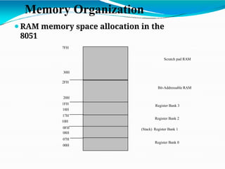
⚫RAM memory spaceallocation in the
8051
7FH
30H
2FH
20H
1FH
10H
0FH
08H
07H
18H
17H
00H
Register Bank 0
(Stack) Register Bank 1
Register Bank 2
Register Bank 3
Bit-Addressable RAM
Scratch pad RAM
Memory Organization
20.
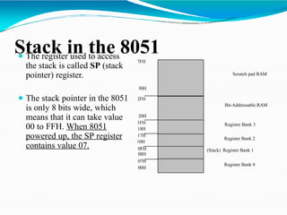
Stack in the8051
⚫ The register used to access
the stack is called SP (stack
pointer) register.
⚫ The stack pointer in the 8051
is only 8 bits wide, which
means that it can take value
00 to FFH. When 8051
powered up, the SP register
contains value 07.
7FH
30H
2FH
20H
1FH
10H
0FH
08H
07H
18H
17H
00H
Register Bank 0
(Stack) Register Bank 1
Register Bank 2
Register Bank 3
Bit-Addressable RAM
Scratch pad RAM
21.
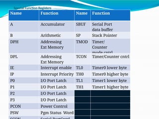
Special Function Registers
NameFunction Name Function
A Accumulator SBUF Serial Port
data buffer
B Arithmetic SP Stack Pointer
DPH Addressing
Ext Memory
TMOD Timer/
Counter
mode cntrl
DPL Addressing
Ext Memory
TCON Timer/Counter cntrl
IE Interrupt enable TL0 Timer0 lower byte
IP Interrupt Priority TH0 Timer0 higher byte
P0 I/O Port Latch TL1 Timer1 lower byte
P1 I/O Port Latch TH1 Timer1 higher byte
P2 I/O Port Latch
P3 I/O Port Latch
PCON Power Control
PSW Pgm Status Word
22.
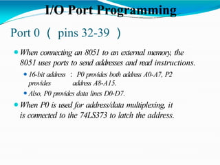
Port 0 (pins 32-39 )
⚫When connecting an 8051 to an external memory, the
8051 uses ports to send addresses and read instructions.
⚫16-bit address : P0 provides both address A0-A7, P2
provides address A8-A15.
⚫Also, P0 provides data lines D0-D7.
⚫When P0 is used for address/data multiplexing, it
is connected to the 74LS373 to latch the address.
I/O Port Programming
23.
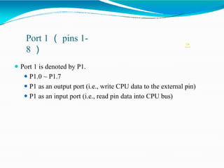
Port 1 (pins 1-
8 )
⚫ Port 1 is denoted by P1.
⚫ P1.0 ~ P1.7
⚫ P1 as an output port (i.e., write CPU data to the external pin)
⚫ P1 as an input port (i.e., read pin data into CPU bus)
24.
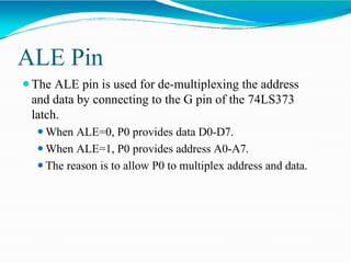
ALE Pin
⚫The ALEpin is used for de-multiplexing the address
and data by connecting to the G pin of the 74LS373
latch.
⚫When ALE=0, P0 provides data D0-D7.
⚫When ALE=1, P0 provides address A0-A7.
⚫The reason is to allow P0 to multiplex address and data.
25.
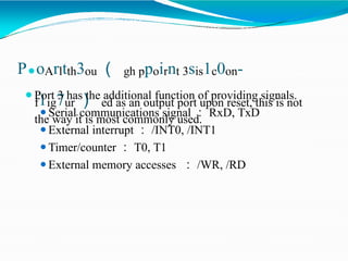
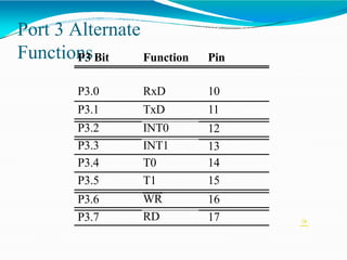
P⚫oArltth3ou ( ghppoirnt 3sis1c0on-
f1ig7ur ) ed as an output port upon reset, this is not
the way it is most commonly used.
⚫Port 3 has the additional function of providing signals.
⚫Serial communications signal : RxD, TxD
⚫External interrupt : /INT0, /INT1
⚫Timer/counter : T0, T1
⚫External memory accesses : /WR, /RD
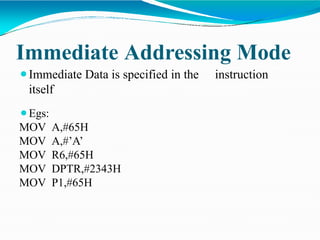
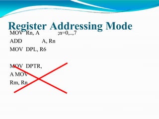
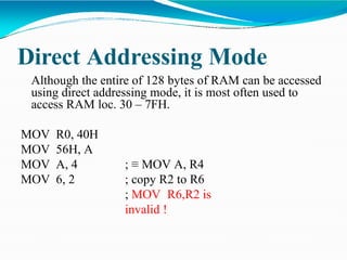
Direct Addressing Mode
Althoughthe entire of 128 bytes of RAM can be accessed
using direct addressing mode, it is most often used to
access RAM loc. 30 – 7FH.
MOV R0, 40H
MOV 56H, A
MOV A, 4
MOV 6, 2
; ≡ MOV A, R4
; copy R2 to R6
; MOV R6,R2 is
invalid !
31.
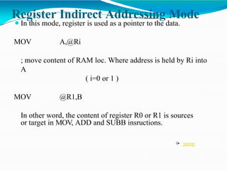
Register Indirect AddressingMode
⚫In this mode, register is used as a pointer to the data.
MOV A,@Ri
; move content of RAM loc. Where address is held by Ri into
A
( i=0 or 1 )
MOV @R1,B
In other word, the content of register R0 or R1 is sources
or target in MOV, ADD and SUBB insructions.
jump
32.
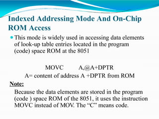
Indexed Addressing ModeAnd On-Chip
ROM Access
⚫This mode is widely used in accessing data elements
of look-up table entries located in the program
(code) space ROM at the 8051
MOVC A,@A+DPTR
A= content of address A +DPTR from ROM
Note:
Because the data elements are stored in the program
(code ) space ROM of the 8051, it uses the instruction
MOVC instead of MOV. The “C” means code.