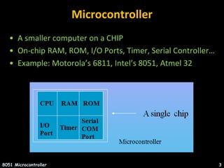
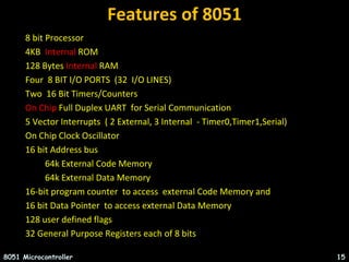
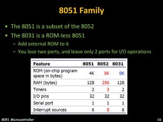
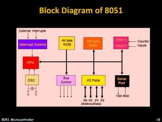
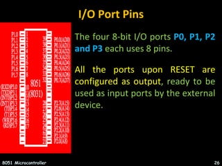
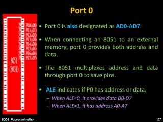
The document discusses microprocessors and microcontrollers. It describes how microprocessors have external RAM, ROM, and I/O ports, while microcontrollers have RAM, ROM, I/O ports, and other components integrated into a single chip. The 8051 microcontroller is presented as a common example that has on-chip memory and I/O in addition to a CPU. Key features of the 8051 such as its memory organization, registers, addressing modes, and instruction set are outlined.


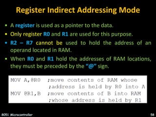
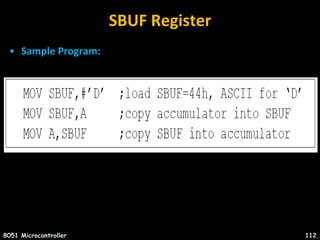
![Internal RAM Structure
Direct &
Indirect
Addressing
Direct
Addressing
Only
SFR [ Special Function
Registers]
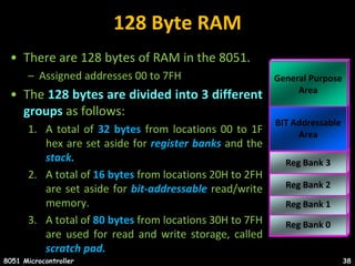
128 Byte Internal RAM
8051 Microcontroller 34
Size: 128 bytes- called
data memory](https://image.slidesharecdn.com/8051-220705073801-dde2fdf1/85/8051-pptx-34-320.jpg)
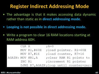
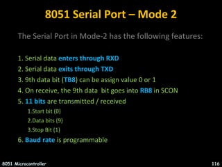
![Special Function Registers [SFR]
8051 Microcontroller 35](https://image.slidesharecdn.com/8051-220705073801-dde2fdf1/85/8051-pptx-35-320.jpg)
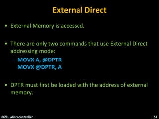
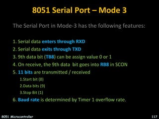
![Program Status Word [PSW]
8051 Microcontroller 36
C AC F0 RS1 RS0 OV F1 P
Register Bank Select
Carry
Auxiliary Carry
User Flag 0
Parity
User Flag 1
Overflow](https://image.slidesharecdn.com/8051-220705073801-dde2fdf1/85/8051-pptx-36-320.jpg)