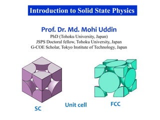
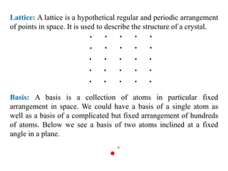
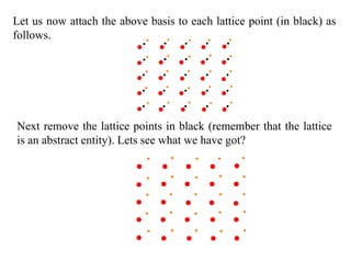
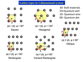
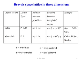
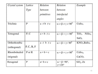
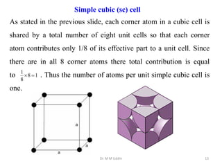
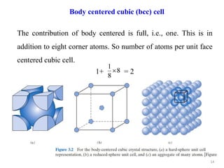
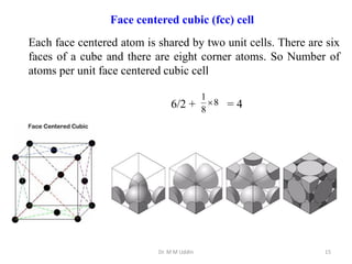
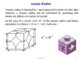
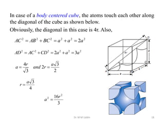
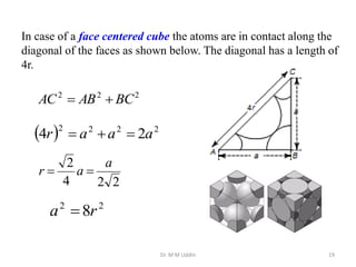
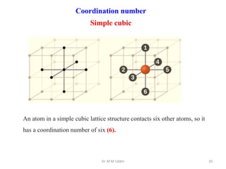
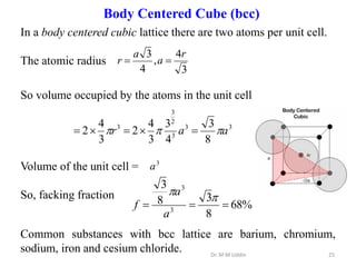
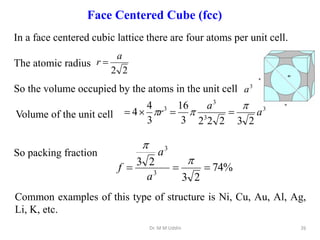
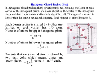
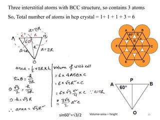
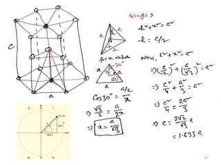
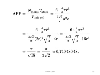
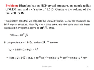
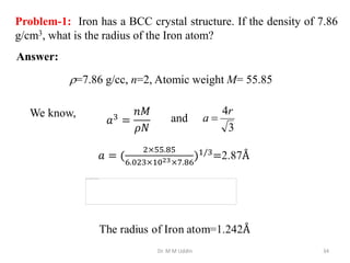
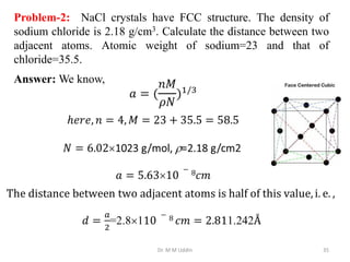
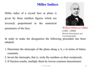
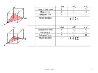
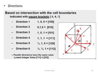
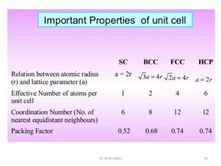
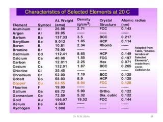
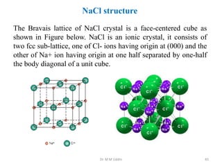
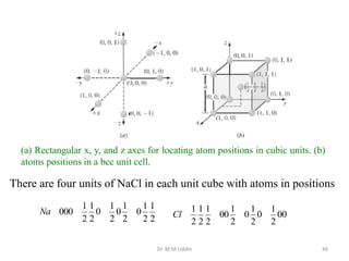
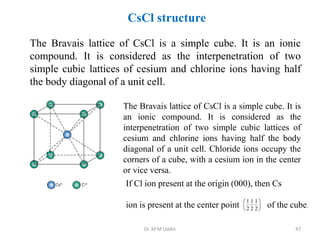
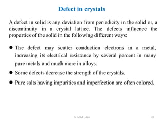
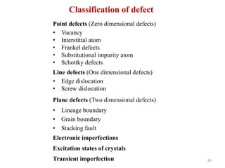
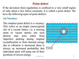
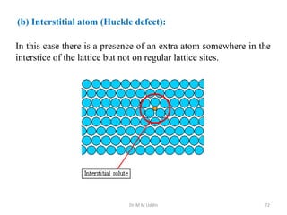
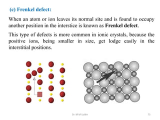
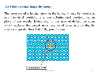
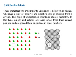
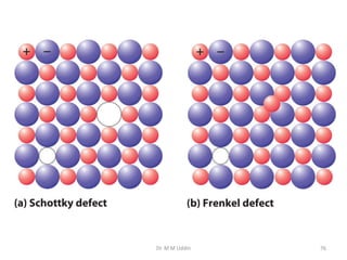
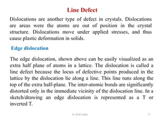
This document provides an introduction to solid state physics and crystallography. It defines key terms like crystalline, non-crystalline, lattice, basis, unit cell and discusses common crystal structures including simple cubic, body centered cubic, and face centered cubic. It also covers topics like Miller indices, atomic packing fraction, coordination number, and examples of crystal structures in sodium chloride and cesium chloride.
- Crystallography is the study of crystalline solids using techniques like X-rays, electron beams, and neutron beams.
- In 1912, Max von Laue proved X-rays were diffracted by crystals, demonstrating diffraction patterns. He received the 1914 Nobel Prize in Physics for this discovery.
- In 1913, father and son team William and Lawrence Bragg developed Bragg's Law to explain X-ray diffraction by crystals and their invention of the X-ray spectroscope earned them the 1914 Nobel Prize in Physics.
- The document discusses different crystal structures including simple cubic, body-centered cubic, face-centered cubic, and hexagonal closely packed.
- Key properties like number of atoms per unit cell, atomic radius, coordination number, and atomic packing factor are defined and calculated for each structure.
- There are seven basic crystal systems that materials can belong to depending on their lattice parameters and angles between axes. The most common systems are cubic, hexagonal, and tetragonal.
This document provides an overview of crystallography and crystal structures. It discusses how crystals form periodic arrangements that can be described by unit cells defined by lattice parameters. The most common crystal structures for metals are face-centered cubic (FCC), body-centered cubic (BCC), and hexagonal close-packed (HCP) since metals form dense, ordered packings with low energies. These crystal structures differ in their unit cell contents and atomic packing factors (FCC has the highest at 0.74). Directions in crystals are described by Miller indices written as [uvw].
This document discusses the atomic arrangement and properties of crystalline solids such as metals. It begins by describing the long-range order in crystalline solids compared to the short-range order in amorphous solids. It then discusses various crystal structures including cubic, hexagonal, and body-centered cubic. It provides examples of calculating properties like atomic packing factor and theoretical density based on crystal structure. Finally, it discusses using X-ray diffraction to determine crystal structure by measuring spacing between crystal planes.
The document discusses different types of solids and crystal structures. It begins by stating that everything around us is matter, which is made of molecules and exists in four main types. It then discusses crystalline and amorphous solids, and the key differences between them. Crystalline solids like metals can have either a single crystal or polycrystalline structure. The document also covers various crystal structures like simple cubic, body centered cubic, face centered cubic, and diamond cubic. It defines important concepts such as unit cell, lattice points, Miller indices, coordination number and packing factor.
This document provides information on crystallography and the structure of crystalline solids. It defines key terms like crystalline solids, amorphous solids, space lattice, unit cell, and Bravais lattices. It describes the primary crystalline structures of metals including simple cubic, body centered cubic, face centered cubic, and hexagonal close packed. It provides details on the characteristics of each structure like atoms per unit cell, coordination number, and packing factor. Crystalline solids are described as having a regular orderly arrangement of atoms compared to the random arrangement in amorphous solids.
The document summarizes key concepts related to crystal structure:
Crystalline materials have atoms or molecules arranged in a regular, orderly 3D pattern which gives them high strength, while non-crystalline materials have a random arrangement and lower strength. A crystal structure is a regular repetition of this 3D pattern defined by a unit cell and space lattice. Common crystal structures include simple cubic, body-centered cubic, face-centered cubic, and hexagonal close-packed. Crystal defects such as point defects, dislocations, grain boundaries, and voids are also discussed.
This document discusses crystal structure and properties of solids. It begins by defining long-range order and crystalline structure, noting that most metals, semiconductors, and some other materials have crystalline structure with atoms arranged in a repetitive grid pattern. It then discusses basic terms like unit cell and space lattice, and describes the seven crystal systems and 14 Bravais lattices. Common metallic crystal structures of body-centered cubic, face-centered cubic, and hexagonal close-packed are discussed. Finally, it touches on X-ray diffraction techniques used to analyze crystal structure.
This document discusses crystal structure and properties of solids. It begins by defining long-range order and crystalline structure, noting that most metals, semiconductors, and some polymers have crystalline structure with atoms arranged in a repetitive grid pattern. It then discusses basic terms like unit cell and space lattice, and describes the seven crystal systems and 14 Bravais lattices. Common metallic crystal structures of body-centered cubic, face-centered cubic, and hexagonal close-packed are discussed. Finally, it touches on X-ray diffraction techniques used to analyze crystal structure.
The document provides guidance on solving numerical problems in solid state chemistry and solutions. It defines key terms and formulas for calculating packing efficiency, unit cell parameters, density, and concentration of solutions. For solid state structures, it explains how to determine the number of atoms in unit cells, radius ratios for coordination number, and formulas for density and efficiency of packing in simple cubic, body centered cubic, and face centered cubic structures. For solutions, it summarizes formulas for molarity, molality, normality, and mole fractions as well as Henry's law and colligative properties.
The study of crystal geometry helps to understand the behaviour of solids and their
mechanical,
electrical,
magnetic
optical and
Metallurgical properties
The document provides information on crystal structures including:
- Crystalline solids have atoms arranged in an orderly, periodic manner while amorphous solids do not.
- Dense, regularly packed structures have lower energy than non-dense, randomly packed structures.
- A unit cell is the smallest repeating unit that defines the lattice structure. There are 14 possible Bravais lattice structures.
- Common crystal structures for metals include body centered cubic (BCC), face centered cubic (FCC), and hexagonal close packed (HCP).
- Properties of unit cells include the number of atoms, effective number of atoms, coordination number, and atomic packing factor.
FellowBuddy.com is a platform which has been setup with a simple vision, keeping in mind the dynamic requirements of students.
Our Vision & Mission - Simplifying Students Life
Our Belief - “The great breakthrough in your life comes when you realize it, that you can learn anything you need to learn; to accomplish any goal that you have set for yourself. This means there are no limits on what you can be, have or do.”
Like Us - https://www.facebook.com/FellowBuddycom-446240585585480
The document provides information about crystal structures, including:
1) It discusses space lattices, which are arrangements of points that repeat periodically in 3D space, with every point having an identical surrounding. The smallest repeating unit of a lattice is called the primitive cell.
2) There are 14 possible crystal structures defined by unique combinations of lattice parameters (a, b, c values and α, β, γ angles). The structures differ in packing efficiency and symmetry.
3) Miller indices are used to specify crystallographic directions and planes, helping to understand properties that vary by orientation like strength and conductivity. Understanding planes and directions is important for predicting deformation and failure modes in materials.
This document provides an overview of a lecture on crystal properties for a semiconductor electronics and devices course. The lecture covers basic definitions of semiconductors, types of semiconductor materials including elemental and compound semiconductors. It also discusses crystal lattices, types of solids, cubic lattices and their types, planes and directions using Miller indices, the diamond lattice structure, and bonding forces in solids including ionic and covalent bonding. The document provides the agenda, content, figures and examples to explain these key concepts.
This document discusses different types of crystal structures including simple cubic, body-centered cubic, face-centered cubic, and hexagonal close-packed. It defines key terms like lattice, unit cell, and coordination number. Simple cubic has a coordination number of 8 and lowest atomic packing factor of 0.52. Body-centered cubic has a coordination number of 8 and packing factor of 0.68. Face-centered cubic has the highest packing factor of 0.74 and coordination number of 12. Hexagonal close-packed is similar to FCC but with a c/a ratio of 1.633. The document also discusses stacking sequences and compares different crystal systems.
The crystal structure notes gives the basic understanding about the different structures crystalline materials and their properties and physics of crystals. It also throw light on the basics of crystal diffraction
The document discusses different types of crystalline solids and their structures. It defines key terms like unit cell, lattice, space lattice, and basis. It describes one, two and three dimensional lattices and the different types of unit cells in two and three dimensions. It also discusses crystal structures, Miller indices for planes and directions, Bravais lattices, and provides examples of rock salt and zinc blende structures.
Crystallography is the experimental science of determining the arrangement of atoms in crystalline solids. Crystallography is a fundamental subject in the fields of materials science and solid-state physics (condensed matter physics). The word crystallography is derived from the Ancient Greek word κρύσταλλος (krústallos; "clear ice, rock-crystal"), with its meaning extending to all solids with some degree of transparency, and γράφειν (gráphein; "to write"). In July 2012, the United Nations recognised the importance of the science of crystallography by proclaiming that 2014 would be the International Year of Crystallography.
The document outlines the syllabus for a semiconductor subject. It includes 15 chapters that cover topics like crystal structure of solids, quantum mechanics, equilibrium carrier transport, pn junctions, bipolar transistors, MOSFETs, and optical and power devices. It also provides details on some key concepts for semiconductors like electrical conductivity and resistivity. Examples are given for different crystal structures including simple cubic, body-centered cubic, and face-centered cubic lattices. Miller indices are introduced for representing crystal planes.
Ic technology- Crystal structure and Crystal growthkriticka sharma
ICs integrate thousands or millions of tiny transistors on a semiconductor wafer. They have advantages over discrete components like being smaller, faster, using less power. Moore's law observes that the number of transistors on an IC doubles every 18 months. Semiconductor substrates are wafers used to fabricate ICs. Crystal defects in wafers like point defects and dislocations can occur during manufacturing and affect processing.
X-ray diffraction is a technique used to determine the atomic structure of crystals. When X-rays hit the periodic lattice of atoms in a crystal, the X-rays diffract into specific directions. This was first discovered by Max von Laue in 1912. Bragg's law quantifies the conditions under which constructive interference, and therefore diffraction, occurs for waves scattered by atomic planes in a crystal. X-ray diffraction methods are now commonly used to analyze crystal structures.
Solid state physics by Dr. kamal Devlal.pdfUMAIRALI629912
This document provides an overview of the course "Solid State Physics" (PHY503). The course covers topics like crystal structure, types of lattices, crystal symmetry, and important crystal structures such as sodium chloride, diamond, and hexagonal close packed. It defines key terms used to describe crystal structure like lattice, basis, unit cell, primitive cell, and Miller indices. It also summarizes different crystal systems and lattice types as well as structural properties of common crystalline materials.
This document discusses the structure of crystalline solids. It begins by defining amorphous and crystalline solids, then introduces fundamental concepts like lattice and unit cell. It describes the structures of common metallic crystals like body centered cubic (BCC), face centered cubic (FCC), and hexagonal close packed (HCP). It also discusses density calculations, polymorphism, crystal systems, Miller indices for directions and planes, and linear and planar atomic densities. Key points covered include unit cell types and properties, coordination numbers, atomic packing factors, and methods for determining Miller indices.
CHINA’S GEO-ECONOMIC OUTREACH IN CENTRAL ASIAN COUNTRIES AND FUTURE PROSPECTjpsjournal1
The rivalry between prominent international actors for dominance over Central Asia's hydrocarbon
reserves and the ancient silk trade route, along with China's diplomatic endeavours in the area, has been
referred to as the "New Great Game." This research centres on the power struggle, considering
geopolitical, geostrategic, and geoeconomic variables. Topics including trade, political hegemony, oil
politics, and conventional and nontraditional security are all explored and explained by the researcher.
Using Mackinder's Heartland, Spykman Rimland, and Hegemonic Stability theories, examines China's role
in Central Asia. This study adheres to the empirical epistemological method and has taken care of
objectivity. This study analyze primary and secondary research documents critically to elaborate role of
china’s geo economic outreach in central Asian countries and its future prospect. China is thriving in trade,
pipeline politics, and winning states, according to this study, thanks to important instruments like the
Shanghai Cooperation Organisation and the Belt and Road Economic Initiative. According to this study,
China is seeing significant success in commerce, pipeline politics, and gaining influence on other
governments. This success may be attributed to the effective utilisation of key tools such as the Shanghai
Cooperation Organisation and the Belt and Road Economic Initiative.
DEEP LEARNING FOR SMART GRID INTRUSION DETECTION: A HYBRID CNN-LSTM-BASED MODELgerogepatton
As digital technology becomes more deeply embedded in power systems, protecting the communication
networks of Smart Grids (SG) has emerged as a critical concern. Distributed Network Protocol 3 (DNP3)
represents a multi-tiered application layer protocol extensively utilized in Supervisory Control and Data
Acquisition (SCADA)-based smart grids to facilitate real-time data gathering and control functionalities.
Robust Intrusion Detection Systems (IDS) are necessary for early threat detection and mitigation because
of the interconnection of these networks, which makes them vulnerable to a variety of cyberattacks. To
solve this issue, this paper develops a hybrid Deep Learning (DL) model specifically designed for intrusion
detection in smart grids. The proposed approach is a combination of the Convolutional Neural Network
(CNN) and the Long-Short-Term Memory algorithms (LSTM). We employed a recent intrusion detection
dataset (DNP3), which focuses on unauthorized commands and Denial of Service (DoS) cyberattacks, to
train and test our model. The results of our experiments show that our CNN-LSTM method is much better
at finding smart grid intrusions than other deep learning algorithms used for classification. In addition,
our proposed approach improves accuracy, precision, recall, and F1 score, achieving a high detection
accuracy rate of 99.50%.
KuberTENes Birthday Bash Guadalajara - K8sGPT first impressionsVictor Morales
K8sGPT is a tool that analyzes and diagnoses Kubernetes clusters. This presentation was used to share the requirements and dependencies to deploy K8sGPT in a local environment.
International Conference on NLP, Artificial Intelligence, Machine Learning an...gerogepatton
International Conference on NLP, Artificial Intelligence, Machine Learning and Applications (NLAIM 2024) offers a premier global platform for exchanging insights and findings in the theory, methodology, and applications of NLP, Artificial Intelligence, Machine Learning, and their applications. The conference seeks substantial contributions across all key domains of NLP, Artificial Intelligence, Machine Learning, and their practical applications, aiming to foster both theoretical advancements and real-world implementations. With a focus on facilitating collaboration between researchers and practitioners from academia and industry, the conference serves as a nexus for sharing the latest developments in the field.
Advanced control scheme of doubly fed induction generator for wind turbine us...IJECEIAES
This paper describes a speed control device for generating electrical energy on an electricity network based on the doubly fed induction generator (DFIG) used for wind power conversion systems. At first, a double-fed induction generator model was constructed. A control law is formulated to govern the flow of energy between the stator of a DFIG and the energy network using three types of controllers: proportional integral (PI), sliding mode controller (SMC) and second order sliding mode controller (SOSMC). Their different results in terms of power reference tracking, reaction to unexpected speed fluctuations, sensitivity to perturbations, and resilience against machine parameter alterations are compared. MATLAB/Simulink was used to conduct the simulations for the preceding study. Multiple simulations have shown very satisfying results, and the investigations demonstrate the efficacy and power-enhancing capabilities of the suggested control system.
Harnessing WebAssembly for Real-time Stateless Streaming PipelinesChristina Lin
Traditionally, dealing with real-time data pipelines has involved significant overhead, even for straightforward tasks like data transformation or masking. However, in this talk, we’ll venture into the dynamic realm of WebAssembly (WASM) and discover how it can revolutionize the creation of stateless streaming pipelines within a Kafka (Redpanda) broker. These pipelines are adept at managing low-latency, high-data-volume scenarios.
ACEP Magazine edition 4th launched on 05.06.2024Rahul
This document provides information about the third edition of the magazine "Sthapatya" published by the Association of Civil Engineers (Practicing) Aurangabad. It includes messages from current and past presidents of ACEP, memories and photos from past ACEP events, information on life time achievement awards given by ACEP, and a technical article on concrete maintenance, repairs and strengthening. The document highlights activities of ACEP and provides a technical educational article for members.
Optimizing Gradle Builds - Gradle DPE Tour Berlin 2024Sinan KOZAK
Sinan from the Delivery Hero mobile infrastructure engineering team shares a deep dive into performance acceleration with Gradle build cache optimizations. Sinan shares their journey into solving complex build-cache problems that affect Gradle builds. By understanding the challenges and solutions found in our journey, we aim to demonstrate the possibilities for faster builds. The case study reveals how overlapping outputs and cache misconfigurations led to significant increases in build times, especially as the project scaled up with numerous modules using Paparazzi tests. The journey from diagnosing to defeating cache issues offers invaluable lessons on maintaining cache integrity without sacrificing functionality.
Using recycled concrete aggregates (RCA) for pavements is crucial to achieving sustainability. Implementing RCA for new pavement can minimize carbon footprint, conserve natural resources, reduce harmful emissions, and lower life cycle costs. Compared to natural aggregate (NA), RCA pavement has fewer comprehensive studies and sustainability assessments.
Recycled Concrete Aggregate in Construction Part III
Crystallography_CE-19.pdf
1. Introduction to Solid State Physics
Unit cell
SC
FCC
Prof. Dr. Md. Mohi Uddin
PhD (Tohoku University, Japan)
JSPS Doctoral fellow, Tohoku University, Japan
G-COE Scholar, Tokyo Institute of Technology, Japan
2. Dr. M M Uddin 2
The science of crystallography is concerned with the enumeration
and classification of all possible types of crystal structures and
determination of the actual structure of the crystalline solids.
Crystalline: Elements and their chemical compounds are found
to occur in three states, i.e., solids, liquids and gases. If the
atoms or molecules in a solid are arranged in some regular
fashion, it is known as crystalline materials.
3. Dr. M M Uddin 3
Non-crystalline or amorphous: When the atoms or molecules
in a solid are arranged in an irregular fashion, it is known as non-
crystalline or amorphous.
In single crystals the same periodicity extends throughout the
material.
4. Dr. M M Uddin 4
Whereas in polycrystalline crystals the same periodicity does not
extend throughout the crystal but is interrupted at grain boundaries.
5. Lattice: A lattice is a hypothetical regular and periodic arrangement
of points in space. It is used to describe the structure of a crystal.
Basis: A basis is a collection of atoms in particular fixed
arrangement in space. We could have a basis of a single atom as
well as a basis of a complicated but fixed arrangement of hundreds
of atoms. Below we see a basis of two atoms inclined at a fixed
angle in a plane.
6. Let us now attach the above basis to each lattice point (in black) as
follows.
Next remove the lattice points in black (remember that the lattice
is an abstract entity). Lets see what we have got?
7. We have got the actual two-dimensional crystal in real space. So
we may write:
lattice + basis = crystal
We have seen that the atomic order in crystalline solids indicates
that the smallest groups of atoms form a repetitive pattern. Thus
in describing crystal structures, it is often convenient to
subdivide the structure into repetitive small repeat entities called
unit cell, i.e. in every crystal some fundamental grouping of
particles is repeated.
Unit cell:
9. 9
Lattice types in 2 dimensional system
3D- Bulk materials
2D-Quantum well
1D- Quantum wire
0D- Quantum dot
10. 10
Optimized InSb QWFET layer structure
Semi-insulator GaAs
Substrate
3 μm Al 0.15In0.85Sb with
Al 0.2In0.8NSb interlayer
45 nm Al 0.15In0.85Sb
Al2O3 ( 10 nm)
In
Gate
InSb (20 nm)
Ec
Ev
11. Dr. M M Uddin 11
Bravais space lattice in three dimensions
C = body-centered
P = primitives
B =base-centered F = face-centered
12. 12
P, C, B, F
Hexagonal P a= b c = =90,
=120
SiO2, Zn
13. Dr. M M Uddin 13
As stated in the previous slide, each corner atom in a cubic cell is
shared by a total number of eight unit cells so that each corner
atom contributes only 1/8 of its effective part to a unit cell. Since
there are in all 8 corner atoms there total contribution is equal
to . Thus the number of atoms per unit simple cubic cell is
one.
Simple cubic (sc) cell
1
8
8
1
14. The contribution of body centered is full, i.e., one. This is in
addition to eight corner atoms. So number of atoms per unit face
centered cubic cell.
1+ = 2
8
8
1
14
Body centered cubic (bcc) cell
15. 8
8
1
Dr. M M Uddin 15
Face centered cubic (fcc) cell
Each face centered atom is shared by two unit cells. There are six
faces of a cube and there are eight corner atoms. So Number of
atoms per unit face centered cubic cell
6/2 + = 4
16. Dr. M M Uddin 16
Example1: A compound formed by elements A and B has a cubic
structure in which A atoms are at the corners of the cube and B
atoms are at face centres. Derive the formula of the compound.
Solution:
As ‘A’ atom are present at the 8 corners of the cube therefore no of
atoms of A in the unit cell = 1/8 × 8 = 1
As B atoms present at the face centres of the cube, therefore no of
atoms of B in the unit cell = 1/2 × 6 = 3
Hence the formula of compound is AB3.
17. Atomic radius is denoted by r and expressed in terms of cube edge
element a. Atomic radius can be calculated by assuming that
atoms are spheres in contact in crystal.
In the case of a simple cube, if r if the atomic radius and lattice
parameter is a then a = 2r or r = a/2. And area
Dr. M M Uddin 17
Atomic Radius
2
2
4r
a
18. In case of a body centered cube, the atoms touch each other along
the diagonal of the cube as shown below.
Obviously, the diagonal in this case is 4r. Also,
2
2
2
2
2
2
2a
a
a
BC
AB
AC
2
2
2
2
2
2
3
2 a
a
a
CD
AC
AD
2
3
2
3
4 a
r
and
r
a
4
3
a
r
Dr. M M Uddin 18
3
16 2
2 r
a
19. In case of a face centered cube the atoms are in contact along the
diagonal of the faces as shown below. The diagonal has a length of
4r.
2
2
2
BC
AB
AC
2
2
2
2
2
4 a
a
a
r
2
2
4
2 a
a
r
2
2
8r
a
Dr. M M Uddin 19
20. Dr. M M Uddin 20
Coordination number
Simple cubic
An atom in a simple cubic lattice structure contacts six other atoms, so it
has a coordination number of six (6).
21. Dr. M M Uddin 21
Body centered cubic (BCC)
Each lattice points has 8 nearest neighbours (in the centers of the neighboured
cubes) and 6 next-nearest neighbours (located at the neighboured vertices of the
lattice). So, the coordination number of BCC is 8.
22. Dr. M M Uddin 22
Face centered cubic (FCC)
Each atom has 12 nearest neighbours (the neighboured face atoms) and 6
next-nearest neighbours (located along the vertices of the lattice). So,
coordination number of FCC/HCP is 12.
23. In a simple cubic (sc) structure the number of atoms per unit cell is
one. The atomic radius is given by half the primitive, i. e., a/2.
So the volume occupied by the atom in the unit cell
3
3
2
3
4
3
4
a
r
23
Atomic packing fraction
The packing fraction is the maximum proportion of the available
volume that can be filled hard spheres.
Or,
The fraction of volume occupied by spherical atoms as compared to
the total available volume of the structure.
24. Dr. M M Uddin 24
Volume of the unit cell = ; so the packing fraction
3
a
Thus the atoms are loosely packed. Polonium at a certain
temperature exhibits such structure.
%
52
6
2
3
4
3
3
a
a
f
f =
𝑣𝑜𝑙𝑢𝑚𝑒 𝑜𝑓 𝑠𝑝ℎ𝑒𝑟𝑒𝑠
𝑣𝑜𝑙𝑢𝑚𝑒 𝑜𝑓 𝑐𝑢𝑏𝑖𝑐
25. In a body centered cubic lattice there are two atoms per unit cell.
The atomic radius
So volume occupied by the atoms in the unit cell
Volume of the unit cell =
So, facking fraction
Common substances with bcc lattice are barium, chromium,
sodium, iron and cesium chloride.
3
4
,
4
3 r
a
a
r
3
3
3
2
3
3
8
3
4
3
3
4
2
3
4
2 a
a
r
%
68
8
3
8
3
3
3
a
a
f
3
a
Dr. M M Uddin 25
Body Centered Cube (bcc)
26. In a face centered cubic lattice there are four atoms per unit cell.
The atomic radius
So the volume occupied by the atoms in the unit cell
Volume of the unit cell
So packing fraction
2
2
a
r
3
3
3
3
2
3
2
2
2
3
16
3
4
4 a
a
r
3
a
%
74
2
3
2
3
3
3
a
a
f
Dr. M M Uddin 26
Common examples of this type of structure is Ni, Cu, Au, Al, Ag,
Li, K, etc.
Face Centered Cube (fcc)
27. Dr. M M Uddin 27
Calculation of lattice constant
Let us consider the case of a cubic lattice of lattice constant a. If
be the density of the crystal then,
Volume of the unit cell=a3
Mass of each unit cell=a3
Let there be n molecules (lattice point) per unit cell, M be the
molecular weight and N be the Avogadro’s number. Then,
------------ (1)
------------ (2)
28. Dr. M M Uddin 28
From equation (1) and (2), we have
------------ (3)
The value of lattice constant a can be calculated using equation (3).
29. Hexagonal Closed Packed (hcp)
In hexagonal closed packed (hcp) structure unit cell contains one atom at each
corner of the hexagonal prism, one atom at each at the center of the hexagonal
faces and three more atoms within the body of the cell. This type of structure is
denser than the simple hexagonal structure. Total number of atoms inside is 6.
Each corner atoms is shared by 6 other unit
lattices or each corner has 1/6 atom.
Number of atoms in upper hexagonal plane
Number of atoms in lower hexagonal plane
We note that each central atom is shared by
two unit cells which means upper and
lower planes contain atom each.
1
6
6
1
1
6
6
1
2
1
2
Dr. M M Uddin
29
30. 30
Three interstitial atoms with BCC structure, so contains 3 atoms
So, Total number of atoms in hcp crystal = 1+ 1 + 1 + 3 = 6
R
R
sin60=3/2 Volume=area height
33. Dr. M M Uddin 33
Problem: Rhenium has an HCP crystal structure, an atomic radius
of 0.137 nm, and a c/a ratio of 1.615. Compute the volume of the
unit cell for Re.
34. Dr. M M Uddin 34
Problem-1: Iron has a BCC crystal structure. If the density of 7.86
g/cm3, what is the radius of the Iron atom?
Answer:
=7.86 g/cc, n=2, Atomic weight M= 55.85
We know,
3
4r
a
and
35. Dr. M M Uddin 35
Answer: We know,
Problem-2: NaCl crystals have FCC structure. The density of
sodium chloride is 2.18 g/cm3. Calculate the distance between two
adjacent atoms. Atomic weight of sodium=23 and that of
chloride=35.5.
36. Miller Indices
Miller index of a crystal face or plane is
given by three smallest figures which are
inversely proportional to the numerical
parameters of the face.
In order to make the designation the following procedure has been
adopted.
1. Determine the intercepts of the plane along a, b, c in terms of lattice
constants.
2. Invert the intercepts, that is, write the numbers as their reciprocals.
3. If fraction results, multiply them by lowest common denominator.
Dr. M M Uddin 36
William Hallowes Miller
(1801 -1880)
British Mineralogist and
Crystallographer
37. 37
The resulting integers are called Miller indices of a plane and conventionally
closed in parentheses (h k l).
The meaning of these indices is that a set of parallel planes (h k l) cuts the a-
axis into h parts, the b-axis into k parts and the c-axis into l parts.
45. NaCl structure
The Bravais lattice of NaCl crystal is a face-centered cube as
shown in Figure below. NaCl is an ionic crystal, it consists of
two fcc sub-lattice, one of Cl- ions having origin at (000) and the
other of Na+ ion having origin at one half separated by one-half
the body diagonal of a unit cube.
Dr. M M Uddin 45
46. (a) Rectangular x, y, and z axes for locating atom positions in cubic units. (b)
atoms positions in a bcc unit cell.
2
1
2
1
0
2
1
0
2
1
0
2
1
2
1
000
Na 00
2
1
0
2
1
0
2
1
00
2
1
2
1
2
1
Cl
There are four units of NaCl in each unit cube with atoms in positions
Dr. M M Uddin 46
47. CsCl structure
The Bravais lattice of CsCl is a simple cube. It is an ionic
compound. It is considered as the interpenetration of two
simple cubic lattices of cesium and chlorine ions having half
the body diagonal of a unit cell.
The Bravais lattice of CsCl is a simple cube. It is
an ionic compound. It is considered as the
interpenetration of two simple cubic lattices of
cesium and chlorine ions having half the body
diagonal of a unit cell. Chloride ions occupy the
corners of a cube, with a cesium ion in the center
or vice versa.
If Cl ion present at the origin (000), then Cs
ion is present at the center point
2
1
2
1
2
1
of the cube.
Dr. M M Uddin 47
48. Bragg’s Law
The Bragg
’s Law is one of most important laws used for
interpreting X-ray diffraction data. In 1913, W. H Bragg and his
son W. L Bragg discovered this law.
Dr. M M Uddin 48
H. L. Bragg
(1862-1942)
W. L. Bragg
(1890-1971)
49. A beam containing X-rays of wavelength is incident upon a crystal at an angle
with a family of Bragg planes whose spacing d. The beam goes past from A in the
first plane and atom C in the next, and each of them scatters part of the beam in
random directions. Constructive interference takes place only between those
scattered rays that are parallel and whose paths differ by exactly , 2, 3 and so
on. That is the path difference must be n, where n is an integer.
Path difference,
BE + EF - AC =BE – AC + EF
=DE+ EF
2
2
2
l
k
h
a
d
10-8 cm
6000/cm
51. sin
EF d
2 sin
DE EF d
2 sin
n d
Constructive Interference:
sin
DE d
where, =wavelength of X-ray
d= spacing of two planes
=scattering angle
n= an integer representing the order of the diffraction peak.
------- (1)
Equation (1) is called Bragg’s law.
52. X-Ray Diffraction (XRD)
How it works?
Philips X-pert Pro X-ray
diffractometer
(Atomic Energy Centre,
Dhaka, AECD)
X-ray diffraction (XRD) is a versatile non-
destructive technique for structure analysis and
phase identification of a wide range of
materials including metals, composites,
polymers, biological materials, electronic and
optoelectronic materials.
Short wavelength X-rays (hard X-rays) in the
range of a few angstroms to 0.1 angstrom (1
keV-120 keV) are used in the diffraction
applications. Because the wavelength of X-rays
is comparable to the size of atoms, they are
ideally suited for probing the structural
arrangement of atoms and molecules in a wide
range of materials.
53. R. Zahir, F.-U.-Z Chowdhury, M.M. Uddin and M.A. Hakim “J.
Magn. Magn. Mater. 410, 55–62 (2016)
Rumana Zahir
University of Central Florida
Florida, USA
54. 20 30 40 50 60 70
x=0.12
x=0.10
x=0.08
x=0.06
x=0.04
x=0.02
Intensity
(a.u.)
2 (degree)
(111)
(220)
(311)
(222)
(400)
(422)
(511) (440)
x=0.00
The XRD patters of the stoichiometric compositions of Co0.5Zn0.5YxFe(2-
x)O4 where (x=0.0, 0.02, 0.04,0.06, 0.10) at Ts=1050C
Mithila Das
University of Coimbra
Coimbra, Portugal
M. Das, M.N.I. Khan, M.A. Matin and M.M. Uddin, Journal of Superconductivity
and Novel Magnetism (2019) (Springer)
55. Characteristic features of Bragg's law
Bragg's law is a consequence of the periodicity of the space lattice.
The law does not refer to the arrangement or basis of atoms associated
with its lattice points.
Bragg reflection can occur only for wavelength 2d. This is the
reason why visible wavelength cannot be used in diffraction.
For the same order and spacing the angle decreases as the
wavelength decreases.
Dr. M M Uddin 55
58. Relation between interplanar spacing d and lattice constant a
Suppose that the plane shown
in figure belongs to a family of
planes whose Miller indices
are (hkl). The perpendicular
ON from origin to the plane
represents the interplanar d of
this family of planes. Let the
direction cosines of ON be
cos, cos, and cos. The
intercepts of the plane of the
three axes are:
Dr. M M Uddin 58
M
B
y
z
a
A
x
C
a
a
a
O
N
59. cos𝛼 =
𝑑ℎ𝑘𝑙
𝑎
ℎ
=
ℎ 𝑑ℎ𝑘𝑙
𝑎
First direction cosine of ON is
𝒅𝒉𝒌𝒍 of crystal with orthogonal axes α = 𝛽 = 𝛾 == 90°
(Cubic, tetragonal, orthorhombic)
a=b=c, a=b≠c a ≠ b≠c
y
z
A
x
C
O
N
B
𝒅𝒉𝒌𝒍 = interplanar spacing between successive hkl planes
passing through the corners of the unit cell
= distance between the origin and the nearest (hkl) plane
ON ⊥ 𝐀𝐁𝐂 (𝒉𝒌𝒍)
60. 60
Second direction cosine of ON is
y
z
A
x
C
O
N
B
cos𝛽 =
𝑑ℎ𝑘𝑙
𝑏
𝑘
=
𝑘 𝑑ℎ𝑘𝑙
𝑏
O
N
B
y
dhkl
𝑏
𝑘
dhkl
𝜸
𝑐
𝑙
Third direction cosine of ON is
cos𝛾 =
𝑑ℎ𝑘𝑙
𝑐
𝑙
=
𝑙 𝑑ℎ𝑘𝑙
𝑐
62. Dr. M M Uddin 62
Tetragonal a=b≠c
Orthorhombic a ≠ b≠c)
63. Dr. M M Uddin 63
Answer:
We know,
2
2
2
l
k
h
a
d
3
1
1
1
111
a
a
d
2 sin
n d
and
64. Problem-5: X-rays of = 0.3 Å are incident on a crystal with lattice
spacing 0.5 Å. Find the angles at which the second and third Bragg's
diffraction maxima are observed.
sin
2d
n
n
n
d
n
3
.
0
sin
10
5
2
10
3
sin
2
sin 11
11
1
1
0
1
9
.
36
6
.
0
sin
2
3
.
0
sin
0
1
64
9
.
0
sin
3
3
.
0
sin
Bragg's equation for X-ray of wavelength is given by
Here, we have = 0.3 Å = 3.0 10-11 m, d = 0.5 Å = 5.0 10-11 m.
Hence,
For, n = 2,
For, n = 3,
64
65. Defect in crystals
The defect may scatter conduction electrons in a metal,
increasing its electrical resistance by several percent in many
pure metals and much more in alloys.
Some defects decrease the strength of the crystals.
Pure salts having impurities and imperfection are often colored.
A defect in solid is any deviation from periodicity in the solid or, a
discontinuity in a crystal lattice. The defects influence the
properties of the solid in the following different ways:
Dr. M M Uddin 65
66. 66
Classification of defect
Point defects (Zero dimensional defects)
• Vacancy
• Interstitial atom
• Frankel defects
• Substitutional impurity atom
• Schottky defects
Line defects (One dimensional defects)
• Edge dislocation
• Screw dislocation
Plane defects (Two dimensional defects)
• Lineage boundary
• Grain boundary
• Stacking fault
Electronic imperfections
Excitation states of crystals
Transient imperfection
67. x = 0.00 x = 0.02
x = 0.04 x = 0.06
FESEM Images of Co0.5Zn0.5YxF2-xO4
67
68. x=0.08
68
0.00 0.02 0.04 0.06 0.08
550
600
650
700
750
800
Grain
size,
D
m
n
m)
Y content, x (wt%)
50 100 150 200 250
0
1
2
3
Resistivity,
/m10
6
)
Temperature,T(C)
x=0.00
x=0.02
x=0.04
x=0.06
x=0.08
-10 -5 0 5 10
-60
-40
-20
0
20
40
60
M
(emu/gm)
Applied field (kOe)
x=0.00
x=0.02
x=0.04
x=0.06
x=0.08
69. Energy Dispersive Spectroscopy Spectra of Co0.5Zn0.5YxF2-xO4
x= 0.00 x = 0.02
Peak obtain for Co, Zn, Y, Fe, O indicate purity of CZYFO.
69
71. If the deviation from regularities is confined to a very small region
of only about a few lattice constants, it is called a point defect. We
have the following types of point defects:
The simplest point defect is a vacancy.
This refers to an empty (unoccupied)
site of a crystal lattice, i.e. a missing
atom or vacant atomic site such
defects may arise either from
imperfect packing during original
crystallization or from thermal energy
due to vibration is increased, there is
always an increased probability that
individual atom will jump out of their
positions of lowest energy. Dr. M M Uddin 71
Point defect
(a) Vacancy:
72. In this case there is a presence of an extra atom somewhere in the
interstice of the lattice but not on regular lattice sites.
Dr. M M Uddin 72
(b) Interstitial atom (Huckle defect):
73. When an atom or ion leaves its normal site and is found to occupy
another position in the interstice is known as Frenkel defect.
This type of defects is more common in ionic crystals, because the
positive ions, being smaller in size, get lodge easily in the
interstitial positions.
Dr. M M Uddin 73
(c) Frenkel defect:
74. The presence of a foreign atom in the lattice. It may be present at
any interstitial position, or at any substitutional position, i.e., in
place of any regular lattice site. In this type of defect, the atom
which replaces the parent atom may be of same size or slightly
smaller or greater than that of the parent atom.
Dr. M M Uddin 74
(d) Substitutional impurity atom:
75. These imperfections are similar to vacancies. This defect is caused,
whenever a pair of positive and negative ions is missing from a
crystal. This type of imperfection maintains charge neutrality. In
this type, anions and cations are taken away from their correct
position and are placed them on surface in equal numbers.
Dr. M M Uddin 75
(e) Schottky defect:
77. Dislocations are another type of defect in crystals. Dislocations
are areas were the atoms are out of position in the crystal
structure. Dislocations move under applied stresses, and thus
cause plastic deformation in solids.
Dr. M M Uddin 77
The edge dislocation, shown above can be easily visualized as an
extra half plane of atoms in a lattice. The dislocation is called a
line defect because the locus of defective points produced in the
lattice by the dislocation lie along a line. This line runs along the
top of the extra half-plane. The inter-atomic bonds are significantly
distorted only in the immediate vicinity of the dislocation line. In a
sketch/drawing an edge dislocation is represented as a T or
inverted T.
Edge dislocation
Line Defect
79. The screw dislocation is slightly more difficult to visualize. The
motion of a screw dislocation is also a result of shear stress, but the
defect line movement is perpendicular to direction of the stress and
the atom displacement, rather than parallel. The screw dislocation is
parallel to the direction in which the crystal is being displaced
(Burgers vector is parallel to the dislocation line).
Dr. M M Uddin 79
Screw dislocation
80. Dr. M M Uddin 80
Plane Defect
A Grain Boundary is a
general planar defect that
separates regions of different
crystalline orientation (i.e.
grains) within a
polycrystalline solid. The
atoms in the grain boundary
will not be in perfect
crystalline arrangement.
Grain boundaries are usually
the result of uneven growth
when the solid is crystallising.
Grain sizes vary from 1 nm to
1 mm.
(a) Grain Boundary
81. Dr. M M Uddin 81
Staking faults are defects in the ‘stacking’
of atomic layers most commonly a fault in
the stacking sequence of the layers, a
missing layer or an added layer, either of
the same type or of a different type with
respect to the bulk layers. Unsurprisingly,
stacking faults are common in layered
structures, but are also encountered in
isotropic structures: in fact, perhaps the best
known type of stacking fault occurs in FCC
metals, and is a fault of
the ...ABCABCABC... stacking sequence
of the (111) layers, as, for example,
in ...ABCABABCABC... Stacking faults.
(b) Staking faults
82. Dr. M M Uddin 82
It is a boundary between two adjacent perfect regions in the
same crystal which are slightly tilted with respect to each other.
(c) Lineage boundary
Ideal crystal Crystal with
lineage boundary
83. Dr. M M Uddin 83
Electronic imperfection
Errors in charge distribution or energy in solids are called
electronic defects. These are defects on a sub-atomic scale which
are responsible for important electrical and magnetic properties.
84. Dr. M M Uddin 84
Excitation states of crystals
Excitation states are quantized things. These are imperfections as
these cause deviations from perfect crystal summary. Some
examples are;
i) Phonons and Magnons which are quantized lattice vibration
and spin waves respectively.
ii) Conduction electrons and holes which are excited thermally
from filled bands or impurity levels.
iii) Excitons which are quantized electron-hole pairs.
iv) Quantized plasma waves.
85. Dr. M M Uddin 85
Transient imperfection
These imperfections are introduce into the crystal from external
sources. e.g.,
i) Photons which are ordinary quantized e.m. waves.
ii) High energy charged particles like, electrons, protons, mesons
and ions.
iii) High energy uncharged particles such as neutrons and neutral
atoms. These imperfections are used in experimental work.
87. Types of Bonding in Solids
Ionic Bonding
Covalent Bonding
Metallic Bonding
Hydrogen Bonding
Van Der Wall’s Bonding
88. An ionic bonding is the Attractive Force existing between positive ion
and a negative ion when they are brought into close proximity or
surrounding.
They are formed when atoms of different elements lose or gain their
electrons in order to achieve stabilized outermost electronic configuration.
Ionic Bond
Ionic Bonding in NaCl
89. Ionic solids are rigid, unidirectional and crystalline in nature.
They have high melting and boiling points.
Ionic solids are good insulators of electricity in their solid state and
good conductor of electricity in their molten state.
Ionic solids are soluble in water and slightly soluble in organic
solvents.
Properties of Ionic bonds
90. A covalent bond is formed, when two or more electrons of an atom, in its
outermost energy level, are shared by other atoms. e.g.-Chlorine molecule.
In this bonding a stable arrangement is achieved by sharing of electrons
rather than transfer of electrons.
Sometimes a covalent bond is also formed when two atoms of different
non-metals share one or more pair of electrons in their outermost energy
level.
e.g.- Water molecule
Covalent Bonds
Bonding between two atoms of same element Bonding between two different non-metals
91. Properties of Covalent bonds
Covalent compounds are bad conductors of electricity.
Covalent compounds are having low melting and boiling points.
Insoluble- in water
Soluble- in organic solvents like Benzene
92. It has been observed that in a metal atoms, the electrons in their
outermost energy levels are loosely held by their nucleii.
Thus a metal may be considered as a cluster of positive ions surrounded
by a large number of free electrons, forming electron cloud.
e.g.- all metals
Metallic Bonds
93. Properties of Metallic bonds
High thermal and electrical conductivity
Low melting and boiling point temperature
Metallic solids are malleable and ductile
94. Hydrogen Bonds
Covalently bonded atoms often produce an Electric dipole
configuration with hydrogen atom as the positive end of the
dipole. If bonds arise as a result of electrostatic attraction between
atoms, it is known as hydrogen bonding.
95. The hydrogen bonds are directional
Relatively strong bonding
These solids have low melting point
No valence electrons hence good insulators
Soluble in both polar and non-polar solvents
They are transparent to light
e.g. – water molecule, ammonic molecules
Properties of Hydrogen Bonds
96. Weak and temporary bonds between molecules of the same
substance are known as Van der Walls bonding.
Types of Van der walls forces
1) dipole-dipole
2) dipole-induced dipole
3) dispersion
Van der walls bonding
97. The main contribution to the binding energy of ionic crystal is
electrostatic and is called the Madelung energy.
Calculation of Medelung constant for NaCl structure
If we take the reference ion as a negative charge, the plus sign will apply
to positive ions and the minus sign to negative ions.