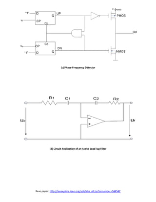
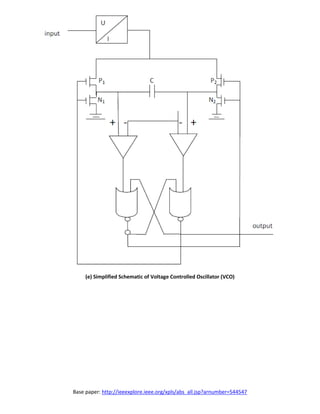
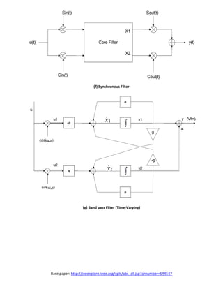
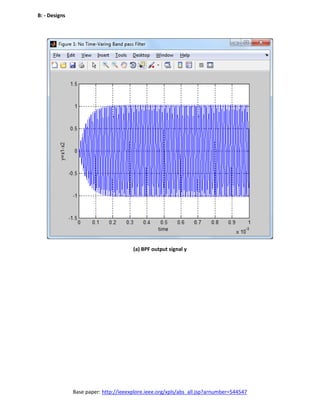
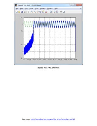
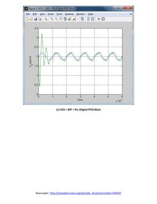
This document discusses the design and implementation of a phase-locked loop (PLL) frequency modulation (FM) demodulator. The key components of the demodulator are the PLL block and an optimum time-varying filter block. The PLL block contains three sub-blocks: a phase-frequency detector, loop filter, and voltage-controlled oscillator. Circuit diagrams and equations for these components are presented. Additionally, a bandpass filter is designed and integrated with the PLL block to improve FM signal quality by recovering the demodulated signal. Simulation results showed the demodulator successfully recovered the FM signal.
Design of all digital phase locked loop (d pll) with fast acquisition timeeSAT Journals
Abstract
A Digital PLL is designed with improved acquisition time and power efficiency. The implemented D-PLL can operate
from 6.54MHz to 105MHz with a power dissipation of is 7.763μW (at 210MHz) with 1.2V supply voltage. The D-PLL is
synthesized using cadence RTL compiler in 45nm CMOS process technology.
Keywords: Digital PLL, Digital Phase/Frequency detector, NCO, Divide by N counter.
Details: https://electronicsembeddedworld.blogspot.com/2018/06/performance-management-mcq.html
FM demodulation involves changing the frequency variations in a signal into amplitude variations at baseband, e.g. audio. There are several techniques and circuits that can be used each with its own advantages and disadvantages.
In any radio that is designed to receive frequency modulated signals there is some form of FM demodulator or detector. This circuit takes in frequency modulated RF signals and takes the modulation from the signal to output only the modulation that had been applied at the transmitter.
There are several types of FM detector / demodulator that can be used. Some types were more popular in the days when radios were made from discrete devices, but nowadays the PLL based detector and quadrature / coincidence detectors are the most widely used as they lend themselves to being incorporated into integrated circuits very easily...
Phase Locked Loop with Filter Banks for High Data Rate Satellite Linkchiragwarty
Satellite communication systems operate in the
presence of path loss and atmospherically induced fading,
which results in waveform distortion, altering phase and bit
time period. After penetrating through several atmospheric
layers, the signal experiences Doppler shift which results in
frequency change and phase reversal, thus to sync the
receiver to the incoming signal we make use of the Phase
Locked Loop (PLL) with a filter at its core functioning.
To recover and reconstruct the original signal, the use of
filter banks in the loop filter block of the PLL will be added
and discussed. The idea of using M-channel uniform filter
banks is to minimize the error by optimizing the
performance in decomposition and reconstruction of signals.
Using different types of fundamental coherent digital
modulation schemes like, M-ary Amplitude/Frequency
/Phase shift keying (MASK, MFSK, MPSK), the best
optimized solution can be determined for all M-channels for
high data rates and bandwidth constraints.
The presentation studies the design of a digital PLL system by
using a variable filter block for several digital modulation
schemes used in ground to space communication links. Two
basic designs will be developed, first model with a fixed set
of filters, those seen in traditional legacy systems and the
second model, which consist of a filtering block made up of
Quadrature Mirror Filter banks (QMF). The method is based
on the strength of the incoming signal and modulation
scheme, which in turn decides the number of filter banks, to
be used to recover the signal.
In this presentation, the focus on pseudo-adaptive nature of the
filter banks is to reconstruct the original signal, considering
the effects of Doppler shift for fast moving airborne
platforms. Subsequently, the comparison between the
performance of the fixed filter based architecture and the
additional design with the variable pseudo-adaptive filter
banks design includes the QMF and Discrete Cosine
Transform Filter banks (DCT). This will follow with the
software oriented simulation of the performance of the
proposed design method, in different scenarios experienced
in satellite links.
Frequency Modulation In Data TransmissionBise Mond
This presentation includes concepts of FM, generation of FM, transmission, reception, with the concepts of stereo FM and some basic circuitry of receiver and transmitter system.
RF Carrier oscillator
To generate the carrier signal.
Usually a crystal-controlled oscillator is used.
Buffer amplifier
Low gain, high input impedance linear amplifier.
To isolate the oscillator from the high power amplifiers.
Modulator : can use either emitter collector modulation
Intermediate and final power amplifiers (pull-push modulators)
Required with low-level transmitters to maintain symmetry in the AM envelope
Coupling network
Matches output impedance of the final amplifier to the transmission line/antenn
Applications are in low-power, low-capacity systems : wireless intercoms, remote control units, pagers and short-range walkie-talkie
Modulating signal is processed similarly as in low-level transmitter except for the addition of power amplifier
Power amplifier
To provide higher power modulating signal necessary to achieve 100% modulation (carrier power is maximum at the high-level modulation point).
Same circuit as low-level transmitter for carrier oscillator, buffer and driver but with addition of power amplifier
Frequency and Power Estimator for Digital Receivers in Doppler Shift Environm...CSCJournals
A frequency estimator well suited for digital receivers is proposed. Accurate estimates of unknown frequency and power of input sinusoidal signal, in the presence of additive white Gaussian noise (AWGN), are provided. The proposed structure solve the problems of traditional phase locked loop (PLL) such as, narrow tracking range, overshoot, long settle time, double frequency ripples in the loop and stability. Proposed method can estimate frequencies up to half the sampling frequency irrespective of the input signal power. Furthermore, it provides stability and allows fast tracking for any changes in input frequency. The estimator is also implemented using field programmable gate array (FPGA), consumes 127 mW and works at a frequency of 225 MHz. Proposed method can estimate the fluctuation in frequency of transmitter’s oscillator, can be used as a frequency shift keying receiver and can also be applied as a digital receiver in Doppler shift environment.
A Low Power Digital Phase Locked Loop With ROM-Free Numerically Controlled Os...CSCJournals
The objective of this paper is to explore the analysis and design of second order digital phase-locked loop (DPLL), and present low power architecture for DPLL. The proposed architecture aims to reduce the high power consumption of DPLL, which results from using a read only memory (ROM) in implementation of the numerically controlled oscillator (NCO). The proposed DPLL utilizes a new design for NCO, in which no ROM is used. DPLL is deigned and implemented using FPGA, consumed 237 mw, which saves more than 25% of power consumption, and works at faster clock frequency compared to traditional architecture.
one of the famous Silicon Valley golden rules which state “Higher the clock frequency, Greater the power consumption”. Digging deep into deep submicron CMOS technology, there are design and power management challenges present for Analog and Mixed Signal devices such as PLL and it is very much important to optimize PLL to create a successful and power optimized system. Here, ALF CP PLL is designed in a way that it can operate on low supply voltage but with a 20% reduction in the overall power consumption. The PLL output frequency can be tuned from 80 MHz to 330 MHz and at 350 MHz PLL consumes 190μW at 1V of supply.
Noise and Bandwidth Consideration in Designing Op-Amp Based Transimpedance Am...journalBEEI
In a visible light communication (VLC) system, there are many modules involved. One of the important modules is Transimpedance Amplifier (TIA) that resides in the analog front-end receiver (Rx-AFE). TIA is responsible for performing signal conversion from current signal, which is provided from the photodiode (PD) to voltage signal. It is the reason why the TIA should be operating in low noise condition and wide bandwidth of frequency. These will enable a flexible coverage of the VLC system in performing its signal processing. Hence, in this research, we provide considerations of the noise and frequency bandwidth analysis in designing TIA to cope with the required design specification of a VLC system.
Spur Reduction Of MB-OFDM UWB System using CMOS Frequency SynthesizerIDES Editor
As Technology progress deeper into submicron
CMOS, traditional analog circuits face problems that are
not to be solved purely by analog innovations. Instead,
new architectures are being proposed which take advantages
of the relatively cheaper of the digital circuits to augment or
improve the diminishing performance of the analog
circuitry. The conventional approach performs the design of
14 bands CMOS frequency synthesizers with spur reduction
for MB-OFMD for analog circuits which have high
distortions and noise. My proposed work is to replace the
analog input PLL into All Digital PLL with spur reduction.
Then the frequency mixing architecture alleviates
harmonics mixing and pulling to diminish spur
generation. The simulation is performed using Model SIM
and the implementation using Microwind to diminish spur
reduction.
A Novel Design of Voltage Controlled Oscillator by Using the Method of Negati...IJECEIAES
The objective of this paper is to develop a new design of a voltage controlled microwave oscillator by using the method of negative resistance in order to fabricate VCO with very good performance in terms of tuning rang, phase noise, output power and stability. The use of hybrid microwave integrated circuit technology’s (HMIC) offers a lot of advantage for our structure concerning size, cost, productivity, and Q factor. This VCO is designed at [480MHz; 1.4GHz] frequency for applications in the phase locked loop (PLL) for signal tracking, FM demodulation, frequency modulation, mobile communication, etc. The different steps of studied voltage controlled oscillator’s design are thoroughly described. Initially designed at a fixed frequency meanwhile the use of a varactor allow us to tune the frequency of the second design. It has been optimized especially regarding tuning bandwidth, power, phase noise, consumption and size of the whole circuit. The achieved results and proposed amendment are the product of theoretical study and predictive simulations with advanced design system microwave design software. A micro-strip VCO with low phase noise based on high gain ultra low noise RF transistor BFP 740 has been designed, fabricated, and characterized. The VCO delivers a sinusoidal signal at the frequency 480 MHz with tuning bandwidth 920 MHz, spectrum power of 12.62 dBm into 50 Ω load and phase noise of -108 dBc/Hz at 100 Hz offset. Measurement results and simulation are in good agreement. Circuit is designed on FR4 substrate which includes integrated resonators and passive components.
International Journal of Engineering Research and Applications (IJERA) is an open access online peer reviewed international journal that publishes research and review articles in the fields of Computer Science, Neural Networks, Electrical Engineering, Software Engineering, Information Technology, Mechanical Engineering, Chemical Engineering, Plastic Engineering, Food Technology, Textile Engineering, Nano Technology & science, Power Electronics, Electronics & Communication Engineering, Computational mathematics, Image processing, Civil Engineering, Structural Engineering, Environmental Engineering, VLSI Testing & Low Power VLSI Design etc.
IJERA (International journal of Engineering Research and Applications) is International online, ... peer reviewed journal. For more detail or submit your article, please visit www.ijera.com
International Journal of Engineering and Science Invention (IJESI)inventionjournals
International Journal of Engineering and Science Invention (IJESI) is an international journal intended for professionals and researchers in all fields of computer science and electronics. IJESI publishes research articles and reviews within the whole field Engineering Science and Technology, new teaching methods, assessment, validation and the impact of new technologies and it will continue to provide information on the latest trends and developments in this ever-expanding subject. The publications of papers are selected through double peer reviewed to ensure originality, relevance, and readability. The articles published in our journal can be accessed online.
Similar to Phase locked loop techniques for fm demodulation and modulation (20)
The Roman Empire A Historical Colossus.pdfkaushalkr1407
The Roman Empire, a vast and enduring power, stands as one of history's most remarkable civilizations, leaving an indelible imprint on the world. It emerged from the Roman Republic, transitioning into an imperial powerhouse under the leadership of Augustus Caesar in 27 BCE. This transformation marked the beginning of an era defined by unprecedented territorial expansion, architectural marvels, and profound cultural influence.
The empire's roots lie in the city of Rome, founded, according to legend, by Romulus in 753 BCE. Over centuries, Rome evolved from a small settlement to a formidable republic, characterized by a complex political system with elected officials and checks on power. However, internal strife, class conflicts, and military ambitions paved the way for the end of the Republic. Julius Caesar’s dictatorship and subsequent assassination in 44 BCE created a power vacuum, leading to a civil war. Octavian, later Augustus, emerged victorious, heralding the Roman Empire’s birth.
Under Augustus, the empire experienced the Pax Romana, a 200-year period of relative peace and stability. Augustus reformed the military, established efficient administrative systems, and initiated grand construction projects. The empire's borders expanded, encompassing territories from Britain to Egypt and from Spain to the Euphrates. Roman legions, renowned for their discipline and engineering prowess, secured and maintained these vast territories, building roads, fortifications, and cities that facilitated control and integration.
The Roman Empire’s society was hierarchical, with a rigid class system. At the top were the patricians, wealthy elites who held significant political power. Below them were the plebeians, free citizens with limited political influence, and the vast numbers of slaves who formed the backbone of the economy. The family unit was central, governed by the paterfamilias, the male head who held absolute authority.
Culturally, the Romans were eclectic, absorbing and adapting elements from the civilizations they encountered, particularly the Greeks. Roman art, literature, and philosophy reflected this synthesis, creating a rich cultural tapestry. Latin, the Roman language, became the lingua franca of the Western world, influencing numerous modern languages.
Roman architecture and engineering achievements were monumental. They perfected the arch, vault, and dome, constructing enduring structures like the Colosseum, Pantheon, and aqueducts. These engineering marvels not only showcased Roman ingenuity but also served practical purposes, from public entertainment to water supply.
Model Attribute Check Company Auto PropertyCeline George
In Odoo, the multi-company feature allows you to manage multiple companies within a single Odoo database instance. Each company can have its own configurations while still sharing common resources such as products, customers, and suppliers.
Ethnobotany and Ethnopharmacology:
Ethnobotany in herbal drug evaluation,
Impact of Ethnobotany in traditional medicine,
New development in herbals,
Bio-prospecting tools for drug discovery,
Role of Ethnopharmacology in drug evaluation,
Reverse Pharmacology.
How to Make a Field invisible in Odoo 17Celine George
It is possible to hide or invisible some fields in odoo. Commonly using “invisible” attribute in the field definition to invisible the fields. This slide will show how to make a field invisible in odoo 17.
The Indian economy is classified into different sectors to simplify the analysis and understanding of economic activities. For Class 10, it's essential to grasp the sectors of the Indian economy, understand their characteristics, and recognize their importance. This guide will provide detailed notes on the Sectors of the Indian Economy Class 10, using specific long-tail keywords to enhance comprehension.
For more information, visit-www.vavaclasses.com
We all have good and bad thoughts from time to time and situation to situation. We are bombarded daily with spiraling thoughts(both negative and positive) creating all-consuming feel , making us difficult to manage with associated suffering. Good thoughts are like our Mob Signal (Positive thought) amidst noise(negative thought) in the atmosphere. Negative thoughts like noise outweigh positive thoughts. These thoughts often create unwanted confusion, trouble, stress and frustration in our mind as well as chaos in our physical world. Negative thoughts are also known as “distorted thinking”.
CLASS 11 CBSE B.St Project AIDS TO TRADE - INSURANCE
Phase locked loop techniques for fm demodulation and modulation
1. Base paper: http://ieeexplore.ieee.org/xpls/abs_all.jsp?arnumber=544547
Phase-Locked Loop Techniques for FM Demodulation and Modulation
Institute of Electrical and Electronics Engineering
Abstract:
Phase locked demodulators are widely used for reception of amplitude modulation(AM), phase
modulation(PM), and frequency modulation(FM). In this research, we concentrated on phase locked FM
demodulators. Our main two parts are the PLL block and the Optimum Time Varying Filter block. We
started our work by building up three basic blocks of the PLL; the PFD, the Loop Filter and the VCO. By
carefully studying the structure and the operation of these blocks, we were able to make good choices
regarding the types of each block and their parameters. As a result, we got the desired results in our PLL
simulations. After that, in order to improve the quality of the FM signal, we worked on the Optimum
Time Varying Filter which is the main research part in the overall thesis. We studied the relationship of
the optimum filter (or matched filter), the optimum time-varying filter and our band pass filter. We then
derived the necessary equations to realize our synchronous filter. Based on the theory and equation
discussion, we were able to design the band pass filter. After we put all of the blocks together to realize
our FM PLL demodulator, we simulated the whole demodulator and recovered the FM demodulated
signal which showed that we had achieved our research goal-namely, to improve the quality of the PLL
FM Demodulator.
11. Base paper: http://ieeexplore.ieee.org/xpls/abs_all.jsp?arnumber=544547
Conclusion:
Phase locked demodulators are widely used for reception of amplitude modulation(AM), phase
modulation(PM), and frequency modulation(FM). In this research, we concentrated on phase locked FM
demodulators. Our main two parts are the PLL block and the Optimum Time Varying Filter block. We
started our work by building up three basic blocks of the PLL; the PFD, the Loop Filter and the VCO. By
carefully studying the structure and the operation of these blocks, we were able to make good choices
regarding the types of each block and their parameters. As a result, we got the desired results in our PLL
simulations. After that, in order to improve the quality of the FM signal, we worked on the Optimum
Time Varying Filter which is the main research part in the overall thesis. We studied the relationship of
the optimum filter (or matched filter), the optimum time-varying filter and our band pass filter. We then
derived the necessary equations to realize our synchronous filter. Based on the theory and equation
discussion, we were able to design the band pass filter. After we put all of the blocks together to realize
our FM PLL demodulator, we simulated the whole demodulator and recovered the FM demodulated
signal which showed that we had achieved our research goal-namely, to improve the quality of the PLL
FM Demodulator.
These results were very satisfying when I finished the simulations. At the same time, I noticed the
distortion problem in the Vcout signal which was affected by the feedback of the band pass filter. The
choice of constant “C” is critical. If I had more time, I would work on this and find a way to get rid of the
Vaudio signal in the BPF feedback and only keep the Vcout signal as part of the feedback. In that case, if
we still could get a good quality FM signal (Vcout), it would be perfect.
References:
D. R. Frey, “Optimal Filtering of AM and FM signal”, submitted to Iscas 2009
D. R. Frey, "Synchronous Filtering", Trans. Circuits and Syst, I: Reg. papers, vol. 53, no. 8, 2006, pp.1772-
1782
D. H. Wolaver, Phase-Locked Loop Circuit Design, Prentice Hall, Englewood Cliffs, NJ, 1991
W. R. Evans, Control-System Dynamics, McGraw-Hill, New York, 1954 H. W. Bode, Network Analysis and
Feedback Amplifier Design, Van Nostrand, New York, 1945
A. Blanchard, Phase-Locked Loops, Wiley, New York, 1976 J.W.M. Bergmans, ”Effect of Loop Delay on
stability of Discrete-time PLL”, IEEE Trans, Circuits & Sys, I, 42, 229-231, Apr.1995