Download to read offline
![International Research Journal of Engineering and Technology (IRJET) e-ISSN: 2395 -0056
Volume: 04 Issue: 01 | Jan -2017 www.irjet.net p-ISSN: 2395-0072
© 2017, IRJET | Impact Factor value: 5.181 | ISO 9001:2008 Certified Journal | Page 880
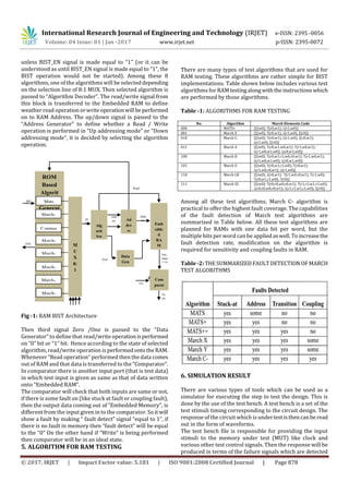
Fig -6: Power Analysis in Xilinx software
Now after the overall designing and testing of the memory,
we will connect it to the FPGA kit through Xilinx software.
The screenshot is shown below:
Fig -7: Connection with FPGA
Figure 8: Connection with FPGA
7. CONCLUSION
This paper presents the design of 512 bitSRAMmemory.We
chose 6T SRAM as memory bit cell and made an array
designed with that bit cell. We came to know many things
about the low power implementation of this 6T SRAM by
going through many papers like making a 7T SRAM or 8T
SRAM. The work in this respect can be taken forward to
make a low power implementation. We have grasped many
important concepts and learned tools that will help us in
future.
In brief, a random access memory with built in self test has
been successfully designed. The BIST techniquesaredivided
as online and offline testing. This project is designed at the
entry level of VHDL so there are lots of modifications that
can be done and additional architecture can be added in
order to increase the robustness of the design.
March C- algorithm can be used in the design by
simply modifying the decoder in our project. This is
done because March C- algorithm is better able to
cover the fault as compared to the otheralgorithms.
We can increase the bit size so that more memory
locations can be tested by us.
BIST is not able to insert the fault model. So future
work can be done in order to insert and then detect
a set of fault models.
We can reduce the hardware coverageofthe project
by replacing the comparator and counter which we
have used. Thus performance of our project will be
improved.
We can replace VHDL with Verilog HDL to reduce
the command line for future work.
Due to non availability of resources, we were not
able to program this project into actual FPGA
hardware. So the future works can be done to run
all these testing through FPGA hardware device to
verify our work.
REFERENCES
[1] Nor Zaidi Haron, Siti AisahMat Junos@Yunus and Amir
Shah Abdul Aziz, “Modeling and Simulation of Microcode
Memory Built-in Self Test Architecture for Embedded
Memories”, Universiti Teknikal Malaysia Melaka.
[2] Shivani Yadav, Neha Malik, Ashutosh Gupta and Sachin
Rajput, “Low Power SRAM Design withReducedRead/Write
Time,” International Journal ofInformationandComputation
Technology, ISSN 0974-2239 Volume 3, Number 3 (2013),
pp. 195-200.
[3] Deepti Kanoujia, Vishal Moyal,“SurveyOnVariousWorks
Done In Reducing Static Power In Various SRAM Cells”,
International Journal Of Technology Enhancements and
Emerging Engineering Research, Vol 2, Issue 11 ISSN 2347 –
4289.](https://image.slidesharecdn.com/irjet-v4i1153-171106082121/85/Performance-Analysis-Designing-and-Testing-512-Bit-Sram-Memory-Chip-Using-Xilinx-Modelsim-Tool-4-320.jpg)
![International Research Journal of Engineering and Technology (IRJET) e-ISSN: 2395 -0056
Volume: 04 Issue: 01 | Jan -2017 www.irjet.net p-ISSN: 2395-0072
© 2017, IRJET | Impact Factor value: 5.181 | ISO 9001:2008 Certified Journal | Page 881
[4] Kalyana Srinivasa Rao, J Venkata Suman PG Student,
Assistant Professor: Department of ECE, GMRIT, Rajam,
Srikakulam, AP, “Low Power Design of A SRAM Cell for
Embedded Memory”, International Journal of Research in
Computer and Communication Technology, Vol 2, Issue 11,
November- 2013.
[5] Preeti S Bellerimath and R. M Banakar, “Implementation
of 16X16 SRAM Memory Array using 180nm Technology”,
International Journal of Current Engineering and
Technology.
[6] Chih-Sheng Hou, Jin-Fu Li, and Ting-Jun Fu, “A BIST
Scheme with the Ability of Diagnostic Data Compression for
RAMs”, IEEE Transactions on Computer-Aided Design of
Integrated Circuits and Systems, Vol. XX. NO. XX, XXXX XXXX
[7] Xu Chuanpei, Tao Yi, Wan Chunting, “BIST method of
SRAM for network-on-chip”, School of Electronic
Engineering and Automatic, Guilin University of Electronic
Technology, Guangxi Key LaboratoryofAutomatic Detecting
Technology and Instruments, Guilin 541004, China.
[8] M.H. Husin, S.Y. Leong, M.F.M. Sabri, R. Nordiana,“Builtin
self test for RAM Using VHDL”, Faculty of Engineering,
Universiti Malaysia Sarawak 94300 Kota Samarahan,
Sarawak.
[9] Ad J. van de Goor, ComTex, Said Hamdioui, Halil Kukner,
“Generic, Orthogonal and Low-cost March Element based
Memory BIST”, Voorwillenseweg 201 2807 CA Gouda, The
Netherlands and Delft University of Technology, Faculty of
EE, Mathematics and CS, Mekelweg 4, 2628 CD Delft, The
Netherlands.
[10] Mária Fischerová, Martin Šimlaštík, “MemBIST Applet
for Learning Principles of Memory Testing and Generating
Memory BIST”, Institute of Informatics, Slovak Academy of
Sciences.
[11] Alberto Bosio, Luigi Dilillo, Patrick Girard, Arnaud
Virazel, Leonardo B. Zordan, “An Effective BIST Architecture
for Power-Gating Mechanisms in Low-Power SRAMs”,
LIRMM, Montpellier, France.
[12] Priyanka Gadde, Mohammed Niamat, “FPGA Memory
Testing Technique using BIST”, Electrical Engineering and
Computer Science Department, The University of Toledo
2801, W. Bancroft, Toledo, Ohio, USA.
[13] P. Manikandan, Bjørn B Larsen, Einar J Aas, Mohammad
Areef, “A Programmable BIST with Macro and Micro codes
for Embedded SRAMs”, The NorwegianUniversityofScience
and Technology, Norway and Juniper Networks, India.
[14] Bharti Mishra, Dr. Rita Jain and Prof. Richa Saraswat,
“Low Power BIST based Multiplier Design and Simulation
using FPGA”, Department of ElectronicsandCommunication
Engineering, LNCT, Rajiv Gandhi Technical University
Bhopal, Madhya Pradesh, India.](https://image.slidesharecdn.com/irjet-v4i1153-171106082121/85/Performance-Analysis-Designing-and-Testing-512-Bit-Sram-Memory-Chip-Using-Xilinx-Modelsim-Tool-5-320.jpg)

This document describes the design and testing of a 512-bit SRAM memory chip using Xilinx/Modelsim tools. The author first designs the SRAM memory using VHDL code and Xilinx tools. Various BIST algorithms like March C- are then implemented to test for faults in the SRAM memory. Simulation results are presented to verify the design and testing of the 512-bit SRAM chip.