Download to read offline
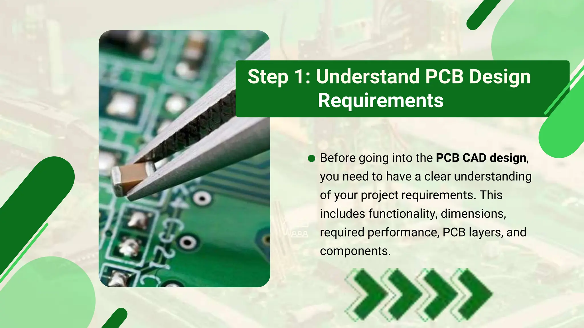


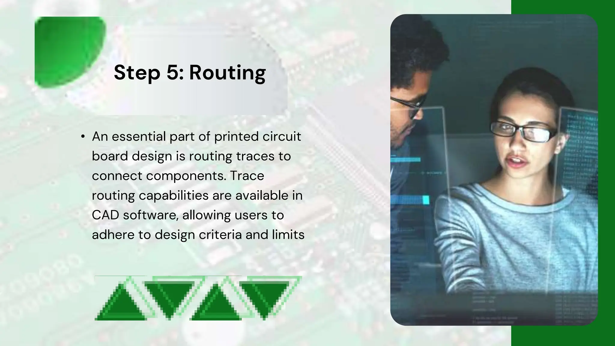
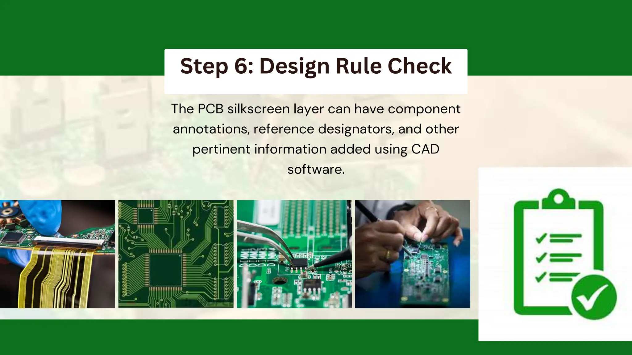


This document is a step-by-step guide for creating PCB CAD design, emphasizing the importance of understanding project requirements, selecting suitable CAD software, and creating accurate component footprints. It outlines essential steps including component placement, routing, design rule checks, and generating manufacturing files and a bill of materials. The guide aims to optimize PCB layout for performance and manufacturability throughout the design process.


