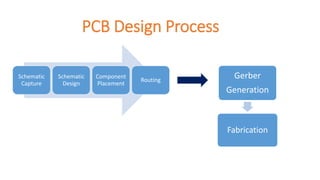
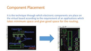
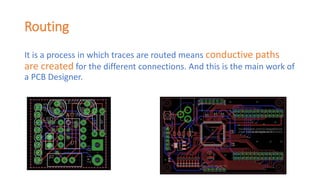
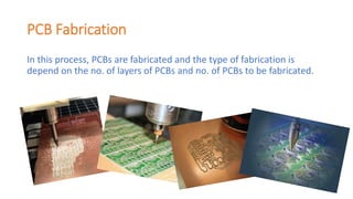
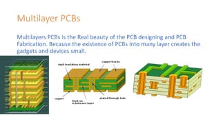
Printed Circuit Boards
and their Designs
What is Printed Circuit Board??
It’s simply known as PCB and actually a board that mechanically
supports and electrical connects electronic
components using conductive tracks, pads and other
features etched from copper sheets laminated onto a non-
conductive substrate. Components (e.g. capacitors, resistors or active
devices) are generally soldered on the PCB.
But in a simple language It is a mechanical solution to an
electrical problem.
Is this a
circuit??
PCB Design Process
Schematic
Capture
Schematic
Design
Component
Placement
Routing
Gerber
Generation
Fabrication
Schematic Capture
It is a process in which exact replica of an electronic component
along with schematic is created in the CAD Software and which known
as the library.
SMD Footprint PTH FootprintSchematic
Schematic Design
Schematic Design is the process in which electronic connections are
done between the different electronic components which is design
according to the application requirement.
Component Placement
It is the technique through which electronic components are place on
the virtual board according to the requirement of an applications which
takes minimum space and give good space for the routing.
Routing
It is a process in which traces are routed means conductive paths
are created for the different connections. And this is the main work of
a PCB Designer.
Points to be Remember
Length of paths should be minimum as possible.
Never take 90 degree turn in routing.
Minimum use of vias and jumpers.
Length of signal paths should be equal.
Gerber Generation
In this process separated files are generated for the each layer and for
every other task which is generally used in PCB(e.g Holes, Organisation
logo, Special Symbols, Mask, Pastes.)
PCB Fabrication
In this process, PCBs are fabricated and the type of fabrication is
depend on the no. of layers of PCBs and no. of PCBs to be fabricated.
Methods of Fabrication
Etching - easy and cost effective
Photographic - for high quality PCBs quickly and efficiently
Multilayer PCBs
Multilayers PCBs is the Real beauty of the PCB designing and PCB
Fabrication. Because the existence of PCBs into many layer creates the
gadgets and devices small.
And the amazing thing about multilayer PCBs is that it can
accommodate up to 16 Layers.
PCB Designing Tools
THANK YOU!

PCB and their Designs

  • 1.
  • 2.
    What is PrintedCircuit Board??
  • 3.
    It’s simply knownas PCB and actually a board that mechanically supports and electrical connects electronic components using conductive tracks, pads and other features etched from copper sheets laminated onto a non- conductive substrate. Components (e.g. capacitors, resistors or active devices) are generally soldered on the PCB.
  • 4.
    But in asimple language It is a mechanical solution to an electrical problem.
  • 5.
  • 6.
  • 7.
    Schematic Capture It isa process in which exact replica of an electronic component along with schematic is created in the CAD Software and which known as the library. SMD Footprint PTH FootprintSchematic
  • 8.
    Schematic Design Schematic Designis the process in which electronic connections are done between the different electronic components which is design according to the application requirement.
  • 9.
    Component Placement It isthe technique through which electronic components are place on the virtual board according to the requirement of an applications which takes minimum space and give good space for the routing.
  • 10.
    Routing It is aprocess in which traces are routed means conductive paths are created for the different connections. And this is the main work of a PCB Designer.
  • 11.
    Points to beRemember Length of paths should be minimum as possible. Never take 90 degree turn in routing. Minimum use of vias and jumpers. Length of signal paths should be equal.
  • 12.
    Gerber Generation In thisprocess separated files are generated for the each layer and for every other task which is generally used in PCB(e.g Holes, Organisation logo, Special Symbols, Mask, Pastes.)
  • 13.
    PCB Fabrication In thisprocess, PCBs are fabricated and the type of fabrication is depend on the no. of layers of PCBs and no. of PCBs to be fabricated.
  • 14.
    Methods of Fabrication Etching- easy and cost effective Photographic - for high quality PCBs quickly and efficiently
  • 15.
    Multilayer PCBs Multilayers PCBsis the Real beauty of the PCB designing and PCB Fabrication. Because the existence of PCBs into many layer creates the gadgets and devices small.
  • 16.
    And the amazingthing about multilayer PCBs is that it can accommodate up to 16 Layers.
  • 17.
  • 18.