Downloaded 93 times

![Introduction to embedded PCB components
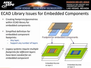
• Embedded PCB Components are components (R’s, C’s,
L’s, IC’s, etc.) that are either formed or placed between
inner layers of a PCB.
• Integration of Embedded PCB Components into the
PCB, also referred to as 3D PCB integration or
technologies, further opens the door to the
miniaturization of electronics.
• Some of these technologies have been in use for over
20 years. However, ongoing advances in
manufacturing capabilities continue to make it easier
to implement in practice.
Trend of Placed Embedded Components for High
Frequency Applications [4]
General technological progression to Embedded Components [9]](https://image.slidesharecdn.com/ipcapex-implementingthelatestembeddedcomponenttechnology-zuken-140430104519-phpapp02/85/Implementing-the-latest-embedded-component-technology-from-concept-to-manufacturing-6-320.jpg)
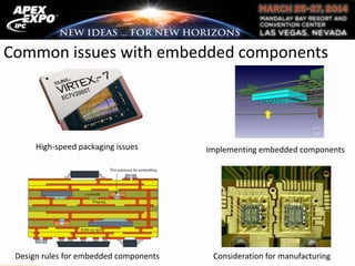
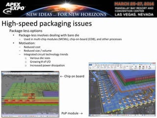
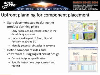
![High-speed packaging issues
Picture: Renesas [12]](https://image.slidesharecdn.com/ipcapex-implementingthelatestembeddedcomponenttechnology-zuken-140430104519-phpapp02/85/Implementing-the-latest-embedded-component-technology-from-concept-to-manufacturing-11-320.jpg)
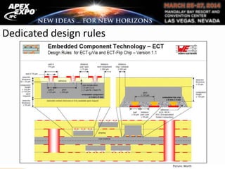
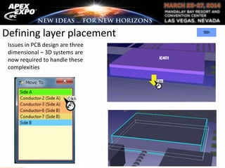
![Placing active components
As more functions are required for the same surface
area, there is a rapid increase in the use of
embedded placed components.
Some component suppliers are producing specialized
low-profile components more suited for embedding
into a PCB.
On the upper right there is a stacked SiP with 4 IC-
dies embedded shown.
In the example right, embedded cores created by
stacking multiple prepreg layers with cavities cut out
for the components. Prepreg layers are stacked until
all components are covered.
Pressure and heat are then applied to cure the
prepreg layers surrounding the components to create
a new core. The core with embedded components
can then be used as building blocks for the rest of
the PCB.
Embedded Component Cores
PCB with two embedded cores [3]
(Picture: FhG-IZM Berli](https://image.slidesharecdn.com/ipcapex-implementingthelatestembeddedcomponenttechnology-zuken-140430104519-phpapp02/85/Implementing-the-latest-embedded-component-technology-from-concept-to-manufacturing-13-320.jpg)
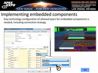
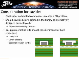
![Placing active components
Two methods of making connects to embedded components are shown below:
1. Solder connection:
This method requires the embedded component to be soldered to an inner layer.
Risk: solder could melt during subsequent processes.
2. Direct via connection:
For this method the component is not soldered to an inner layer trace but rather connected directly to a via.
Benefit: further reduction in trace length.
Risk: the embedded component could be damaged during blind via laser drilling or during via plating.
From the limitations provided above, it should be clear that manufacturability is a key
limiting factor in the use of embedded placed components. Ongoing improvements in
manufacturability are being pursued to address these concerns.
Embedded PCB Connections for a Placed Capacitor [7]](https://image.slidesharecdn.com/ipcapex-implementingthelatestembeddedcomponenttechnology-zuken-140430104519-phpapp02/85/Implementing-the-latest-embedded-component-technology-from-concept-to-manufacturing-14-320.jpg)


This document discusses implementing embedded components in printed circuit boards from concept to manufacturing. It begins with an overview of embedded component technologies and their advantages like increased density and performance. Common challenges are then addressed such as meeting tolerance requirements for formed components and impact on thermal behavior. The document emphasizes the importance of considering manufacturability early in the design process and working closely with manufacturers to define dedicated design rules. It concludes that a true 3D design approach is necessary to effectively implement embedded component technologies.