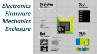
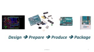
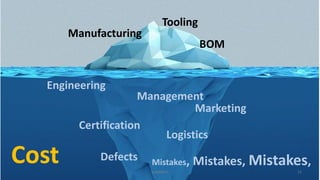
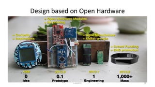
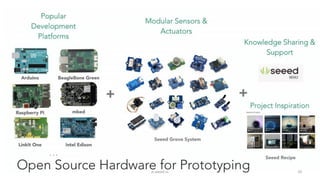
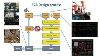
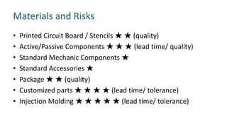
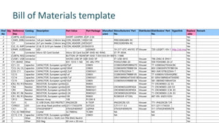
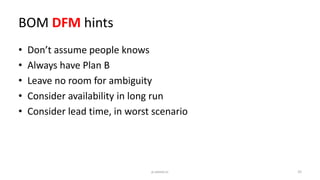
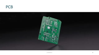
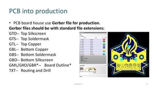
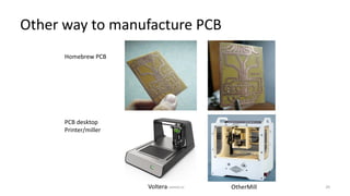
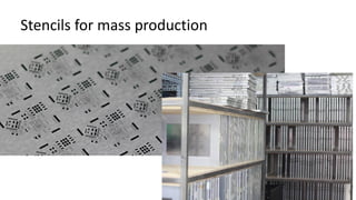
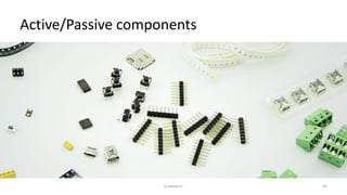
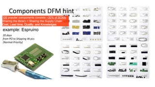
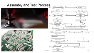
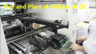
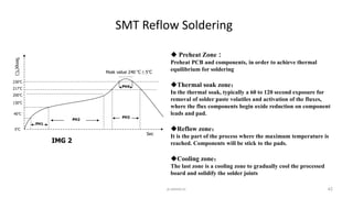
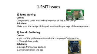
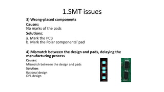
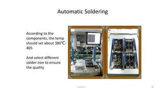
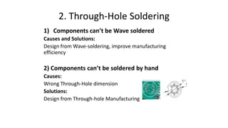
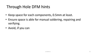
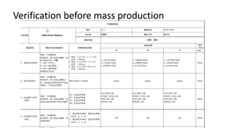
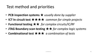
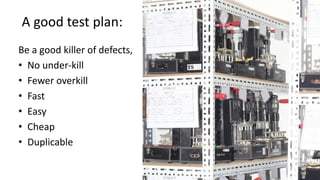
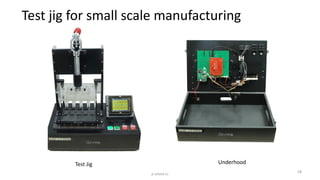
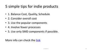
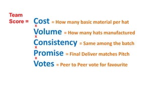
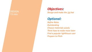
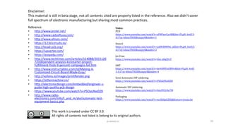
1
Electronic
Manufacturing Eric Pan
seeed.cc
p.seeed.cc
Eric Pan
Maker, Biker
Founder of Seeed
3
Chapter 0
Overview
p.seeed.cc
Today’s Sharing
4p.seeed.cc
HOW?
5p.seeed.cc
6
Electronics
Firmware
Mechanics
Enclosure
p.seeed.cc
Design  Prepare  Produce  Package
7p.seeed.cc
Cost * Quality * Schedule
8p.seeed.cc
Quality
p.seeed.cc 9
Expectations
Schedule
ALL shall arrive on time.
But,
- Supply chain is very dynamic
- Production line has queue
- Problems are unexpected
Project Management is
Serious.
p.seeed.cc 10
11p.seeed.cc
Cost
BOM
Manufacturing
Engineering
Marketing
Certification
Logistics
Defects
Management
Mistakes, Mistakes, Mistakes,
Tooling
12
Chapter 1
Design from manufacture
p.seeed.cc
Be Responsible For what you started.
p.seeed.cc 14
https://en.wikipedia.org/wiki/Design_for_X
Development phase
Design for short time to market
Design for reliability
Design for test
Design for safety
Design for quality
Design against corrosion damage
Design for minimum risk
Production-operations phase
Design to cost
Design to standards
Design for assembly
Design for manufacturability
Design for logistics
Design for postponement
Design for Electronic Assemblies
Design for Low-Quantity Production
Use phase
Design for user-friendliness
Design for ergonomics
Design for aesthetics
Design for serviceability
Design for maintainability
Design for repair-reuse-recyclability
Disposal phase
Design for Environment
Design for recycling
Design for Remanufacturing)
Design for X
15
Hardware
Orchestra
Software
Band
Unarmed to the new field.
p.seeed.cc 16
https://en.wikipedia.org/wiki/Design_for_X
Development phase
Design for short time to market
Design for reliability
Design for test
Design for safety
Design for quality
Design against corrosion damage
Design for minimum risk
Production-operations phase
Design to cost
Design to standards
Design for assembly
Design for manufacturability
Design for logistics
Design for postponement
Design for Electronic Assemblies
Design for Low-Quantity Production
Use phase
Design for user-friendliness
Design for ergonomics
Design for aesthetics
Design for serviceability
Design for maintainability
Design for repair-reuse-recyclability
Disposal phase
Design for Environment
Design for recycling
Design for Remanufacturing)
Design for X
17
Design FROM
Manufacturing
700+ popular components
Open testing/Open process/Open
manufacturing capability/Open schedule
3D printer/Laser
cutting/CNC/Automated SMT
line/flexible cell line/Tools
500+ different kinds of module for
MCU/Sensors/Shield/Prototyping/To
ols/Wearables…
Open Parts Library for
Supply Chain
Open Source Hardware for
Prototyping
Open Manufacturing for Process
Distributed Manufacturing
as a Service
1
2 3
4
Design based on Open Hardware
18p.seeed.cc
19p.seeed.cc
20p.seeed.cc
Beginner
Professional
Expensive Free
More
Free,
Cloud based
Collaborative
CAD tools
21p.seeed.cc
PCB Design process
22
Chapter 2
Prepare the materials
p.seeed.cc
Materials and Risks
• Printed Circuit Board / Stencils ★ ★ (quality)
• Active/Passive Components ★ ★ ★ (lead time/ quality)
• Standard Mechanic Components ★
• Standard Accessories ★
• Package ★ ★ (quality)
• Customized parts ★ ★ ★ ★ (lead time/ tolerance)
• Injection Molding ★ ★ ★ ★ ★ (lead time/ tolerance)
Bill of Materials template
BOM DFM hints
• Don’t assume people knows
• Always have Plan B
• Leave no room for ambiguity
• Consider availability in long run
• Consider lead time, in worst scenario
25p.seeed.cc
PCB
26p.seeed.cc
• PCB board house use Gerber file for production.
Gerber files should be with standard file extensions:
GTO-- Top Silkscreen
GTS-- Top Soldermask
GTL-- Top Copper
GBL-- Bottom Copper
GBS-- Bottom Soldermask
GBO-- Bottom Silkscreen
GML/GKO/GBR*-- Board Outline*
TXT-- Routing and Drill
PCB into production
27p.seeed.cc
28p.seeed.cc
Other way to manufacture PCB
PCB desktop
Printer/miller
Homebrew PCB
Voltera OtherMill 29p.seeed.cc
PCB DFM hint
• Follow supplier process spec, leave some buffer if possible
• Polarized component must be marked.
• Designator for each components.
• Silkscreen must be clear. 6mil width, 40mil height.
30p.seeed.cc
Stencils for mass production
p.seeed.cc 31
Active/Passive components
32p.seeed.cc
example: Espruino
20 days
from PO to Shipping 4k pcs
(Normal Priority)
100 popular components consists ~30% of BOMs
Sharing the library = Sharing the Supply Chain
Cost, Lead time, Quality, and Knowledges
Components DFM hint
Standard Accessories
34p.seeed.cc
Package
35p.seeed.cc
Customized Parts
36p.seeed.cc
Injection Molding
37p.seeed.cc
38
Chapter 3
Assembly
p.seeed.cc
Assembly and Test Process
Y
Y
Y
Stencil print paste
SMT
SMT Assembly
DIP Assembly
PCB incoming inspection
Print quality check
QC check before
reflow Owen
Assembly quality check
Functional check
Assembly quality check
IQC check
Clean
Inform Engineer improve
I PQC confirm
Repairing
Adjustment
Inform engineer improve
Remove components
FQC
Repairing
Y
Y
Y
Y
N
N
N
N
N
N
N
N
Y
Inform engineer improve
39p.seeed.cc
40p.seeed.cc
Solder Paste Screen Printing
41p.seeed.cc
Pick and Place  Reflow  QC
40℃
130℃
200℃
217℃
230℃
0℃
PH1
PH2
PH3
PH4
Peak value 240 ℃±5℃
Sec
Temp(℃)
IMG 2
42
SMT Reflow Soldering
p.seeed.cc
 Preheat Zone:
Preheat PCB and components, in order to achieve thermal
equilibrium for soldering
Thermal soak zone:
In the thermal soak, typically a 60 to 120 second exposure for
removal of solder paste volatiles and activation of the fluxes,
where the flux components begin oxide reduction on component
leads and pad.
Reflow zone:
It is the part of the process where the maximum temperature is
reached. Components will be stick to the pads.
Cooling zone:
The last zone is a cooling zone to gradually cool the processed
board and solidify the solder joints
1) Tomb stoning
Causes:
Components don’t match the dimension of the actual design
Solutions:
Make sure the design of the pad matches the package of the components
2) Pseudo Soldering
Causes:
a. pitch of the pad does not match the component’s dimension
b. Through-hole pads
Solutions:
a. design from actual package
b. avoid via hole of the pad
1.SMT issues
1.SMT issues
3) Wrong-placed components
Causes:
No marks of the pads
Solutions:
a. Mark the PCB
b. Mark the Polar components’ pad
4) Mismatch between the design and pads, delaying the
manufacturing process
Causes:
Mismatch between the design and pads
Solution:
Rational design
OPL design
SMT DFM hints
• Compassion for machines
• Align same components in order
• Leave adequate spacing for thermal parts
• Leave enough margin to PCB edge
• Avoid double side placement if possible
45p.seeed.cc
46p.seeed.cc
Through Hole Soldering
Semi Auto Through Hole Soldering
Temperature should set 300℃+-10℃, Flux spraying evenly for
3-4 seconds, dry for 2-4 seconds, move the PCB into the tin
surface for 3-4 seconds, then move it to the cooing zone.
47p.seeed.cc
Automatic Soldering
48
According to the
components, the temp
should set about 380℃-
405
And select different
solder iron to ensure
the quality
p.seeed.cc
49p.seeed.cc
1) Components can’t be Wave soldered
Causes and Solutions:
Design from Wave-soldering, improve manufacturing
efficiency
2) Components can’t be soldered by hand
Causes:
Wrong Through-Hole dimension
Solutions:
Design from Through-hole Manufacturing
2. Through-Hole Soldering
3)Short distance between two components
Causes and Solutions:
Ensure Standard distance between two through-holes
4)Tilted parts after wave-soldering
Causes and Solutions:
Design from the wave-soldering standard
• Keep space for each components, 0.5mm at least.
• Ensure space is able for manual soldering, repairing and
verifying.
• Avoid, if you can
Through Hole DFM hints
52p.seeed.cc
53
Chapter 4
Test and Package
p.seeed.cc
Basically,
Verification before mass production
• PCB inspection systems ★ usually done by supplier
• ICT In circuit test ★★★★ common for simple projects
• Functional testing ★★ for complex circuits/IC/RF
• JTAG Boundary scan testing ★★ for complex logic systems
• Combinational test ★★★ a combination of tests
Test method and priorities
56p.seeed.cc
Be a good killer of defects,
• No under-kill
• Fewer overkill
• Fast
• Easy
• Cheap
• Duplicable
A good test plan:
57p.seeed.cc
Test jig for small scale manufacturing
p.seeed.cc
58
Test Jig Underhood
59p.seeed.cc
Packaging with SOP
3. PCB Testing Process
1)Can’t make test jig
Causes:
No test feasibility plan before design
Solutions:
Consider test plan before design
2) No test plan
Solutions:
Provide test plan before new product introduction
1) Unable or difficult to assembly.
Causes:
Do not verify the mechanical part after designing.
Solutions:
Should consider tolerance, and verify the mechanical part.
4. Assembly Process
1) Uncertain packaging
Causes and Solutions:
Customer do not have packaging nearly production. IT should be prepared in the
designing stage.
2) Unreasonable packaging method
Causes:
Unable to pack according to the packaging method
Solutions:
Should confirm Packaging method beforehand
5. Packaging
Assembly and Test hints
• Try to involve less process
• SOP (standard operation procedure) is critical
• Invent when there is no other choices
• Don’t expect Pilot run will expose every error
• Wherever might be problem, there will be problem.
p.seeed.cc 63
64
Chapter 5
Takeaways
p.seeed.cc
65
Setup
7-42 days
Manufacturing
3-15 days
Engineering
1-30 days
• Unclear BOM
• Process Tolerance
• Inadequate Test Plan
• Long Lead Time Components
• Consistency Problem
• Supply Chain Complexity
• Unexpected Error
• Low Yield
• Uncontrollable Assembly Time
Prototype Product
manufacture
Key Phrases and Risks
66p.seeed.cc
Maker Supplier
5 simple tips for indie products
• 1. Balance Cost, Quality, Schedule
• 2. Consider overall cost
• 3. Use the popular components
• 4. Involve fewer processes
• 5. Use only SMD components if possible.
More info can check the link
67p.seeed.cc
68
Chapter 6
Practice
p.seeed.cc
Let’s redefine hat
Cost = How many basic material per hat
Volume = How many hats manufactured
Consistency = Same among the batch
Promise = Final Deliver matches Pitch
Votes = Peer to Peer vote for favourite
Team
Score =
x
x
x
x
Basic Components
20 pcs A4 paper, 1*Adhesive tape,
Shared components
Anything you can find(legally)
Equipment
1*Scissors, 1*Stapler, 2*Colors pens,
Design – Pitch – Manufacture – Deliver
DESIGN
15 min
PITCH
2 min
MANUFACTURE
20 min
DELIVER
5 min
DESIGN
15 min
Objectives:
Design and make the 1st hat
Optional:
Define Roles
Outstanding
Choose materials wisely
Think how to make more later
Find a popular lighthouse user
Prepare to Pitch
PITCH
2 min
Objectives:
Sell your design to backers
Optional:
AWESOME!
MANUFACTURE
20 min
Objectives:
Manufacture more hats!
Optional:
Collect enough material
Prepare a operation procedure
Optimize the process
Apply Quality Control
Objectives:
Show us the results!
Optional:
A moving story
Improvement (downgrade) applied
Share your hints
DELIVER
5 min
A free fusion PCB coupon for the submitter
A free fusion PCBA coupon for the winner
Share your result photo/thoughts
via twitter @seeedstudio #fusion, to
win
Diving by sport in touch UK, from Pinterest
Good Luck
To the mass
78p.seeed.cc
This work is created under CC BY 3.0
All rights of contents not listed is belong to its original authors.
79p.seeed.cc
Disclaimer:
This material is still in beta stage, not all contents cited are properly listed in the reference. Also we didn’t cover
full spectrum of electronic manufacturing but sharing most common practices.
Video:
PCB
https://www.youtube.com/watch?v=sFMFmrCur08&list=PLpH_4mf13-
A17zy-k0oiaTNSXBisxqxyR&index=1
Stencil
https://www.youtube.com/watch?v=ya8N4RWNo_s&list=PLpH_4mf13-
A17zy-k0oiaTNSXBisxqxyR&index=3
Jet Print
https://www.youtube.com/watch?v=Voe-z0qCEvY
SMT
https://www.youtube.com/watch?v=6e4AMTmURVw&list=PLpH_4mf1
3-A17zy-k0oiaTNSXBisxqxyR&index=4
Semi Automatic DIP soldering
https://www.youtube.com/watch?v=PSOaUNxIDZ8
Automatic DIP soldering
https://www.youtube.com/watch?v=fmvFO3rfw7M
Packaging
https://www.youtube.com/watch?v=mrZOSpGZliQ&feature=youtu.be
Reference
• http://www.protel.net/
• http://www.cadsoftusa.com/
• http://www.altium.com/
• https://123d.circuits.io/
• http://kicad-pcb.org/
• https://upverter.com/
• https://easyeda.com/
• http://www.techtimes.com/articles/114088/2015120
7/independent-analysis-kickstarter-project-
fulfillment-finds-9-percent-campaigns-fail.htm
• http://www.instructables.com/id/Making-A-
Customized-Circuit-Board-Made-Easy/
• http://voltera.io/images/printRender.png
• https://othermachine.co/
• http://electronicdesign.com/embedded/engineer-s-
guide-high-quality-pcb-design
• https://www.youtube.com/watch?v=PSOaUNxIDZ8
• http://www.radio-
electronics.com/info/t_and_m/ate/automatic-test-
equipment-basics.php

Electronic manufacturing v3.0 - Fab Academy 2016

  • 1.
  • 2.
  • 3.
  • 4.
  • 5.
  • 6.
  • 7.
    Design  Prepare Produce  Package 7p.seeed.cc
  • 8.
    Cost * Quality* Schedule 8p.seeed.cc
  • 9.
  • 10.
    Schedule ALL shall arriveon time. But, - Supply chain is very dynamic - Production line has queue - Problems are unexpected Project Management is Serious. p.seeed.cc 10
  • 11.
  • 12.
    12 Chapter 1 Design frommanufacture p.seeed.cc
  • 13.
    Be Responsible Forwhat you started.
  • 14.
    p.seeed.cc 14 https://en.wikipedia.org/wiki/Design_for_X Development phase Designfor short time to market Design for reliability Design for test Design for safety Design for quality Design against corrosion damage Design for minimum risk Production-operations phase Design to cost Design to standards Design for assembly Design for manufacturability Design for logistics Design for postponement Design for Electronic Assemblies Design for Low-Quantity Production Use phase Design for user-friendliness Design for ergonomics Design for aesthetics Design for serviceability Design for maintainability Design for repair-reuse-recyclability Disposal phase Design for Environment Design for recycling Design for Remanufacturing) Design for X
  • 15.
  • 16.
    p.seeed.cc 16 https://en.wikipedia.org/wiki/Design_for_X Development phase Designfor short time to market Design for reliability Design for test Design for safety Design for quality Design against corrosion damage Design for minimum risk Production-operations phase Design to cost Design to standards Design for assembly Design for manufacturability Design for logistics Design for postponement Design for Electronic Assemblies Design for Low-Quantity Production Use phase Design for user-friendliness Design for ergonomics Design for aesthetics Design for serviceability Design for maintainability Design for repair-reuse-recyclability Disposal phase Design for Environment Design for recycling Design for Remanufacturing) Design for X
  • 17.
    17 Design FROM Manufacturing 700+ popularcomponents Open testing/Open process/Open manufacturing capability/Open schedule 3D printer/Laser cutting/CNC/Automated SMT line/flexible cell line/Tools 500+ different kinds of module for MCU/Sensors/Shield/Prototyping/To ols/Wearables… Open Parts Library for Supply Chain Open Source Hardware for Prototyping Open Manufacturing for Process Distributed Manufacturing as a Service 1 2 3 4
  • 18.
    Design based onOpen Hardware 18p.seeed.cc
  • 19.
  • 20.
  • 21.
  • 22.
    22 Chapter 2 Prepare thematerials p.seeed.cc
  • 23.
    Materials and Risks •Printed Circuit Board / Stencils ★ ★ (quality) • Active/Passive Components ★ ★ ★ (lead time/ quality) • Standard Mechanic Components ★ • Standard Accessories ★ • Package ★ ★ (quality) • Customized parts ★ ★ ★ ★ (lead time/ tolerance) • Injection Molding ★ ★ ★ ★ ★ (lead time/ tolerance)
  • 24.
  • 25.
    BOM DFM hints •Don’t assume people knows • Always have Plan B • Leave no room for ambiguity • Consider availability in long run • Consider lead time, in worst scenario 25p.seeed.cc
  • 26.
  • 27.
    • PCB boardhouse use Gerber file for production. Gerber files should be with standard file extensions: GTO-- Top Silkscreen GTS-- Top Soldermask GTL-- Top Copper GBL-- Bottom Copper GBS-- Bottom Soldermask GBO-- Bottom Silkscreen GML/GKO/GBR*-- Board Outline* TXT-- Routing and Drill PCB into production 27p.seeed.cc
  • 28.
  • 29.
    Other way tomanufacture PCB PCB desktop Printer/miller Homebrew PCB Voltera OtherMill 29p.seeed.cc
  • 30.
    PCB DFM hint •Follow supplier process spec, leave some buffer if possible • Polarized component must be marked. • Designator for each components. • Silkscreen must be clear. 6mil width, 40mil height. 30p.seeed.cc
  • 31.
    Stencils for massproduction p.seeed.cc 31
  • 32.
  • 33.
    example: Espruino 20 days fromPO to Shipping 4k pcs (Normal Priority) 100 popular components consists ~30% of BOMs Sharing the library = Sharing the Supply Chain Cost, Lead time, Quality, and Knowledges Components DFM hint
  • 34.
  • 35.
  • 36.
  • 37.
  • 38.
  • 39.
    Assembly and TestProcess Y Y Y Stencil print paste SMT SMT Assembly DIP Assembly PCB incoming inspection Print quality check QC check before reflow Owen Assembly quality check Functional check Assembly quality check IQC check Clean Inform Engineer improve I PQC confirm Repairing Adjustment Inform engineer improve Remove components FQC Repairing Y Y Y Y N N N N N N N N Y Inform engineer improve 39p.seeed.cc
  • 40.
  • 41.
    41p.seeed.cc Pick and Place Reflow  QC
  • 42.
    40℃ 130℃ 200℃ 217℃ 230℃ 0℃ PH1 PH2 PH3 PH4 Peak value 240℃±5℃ Sec Temp(℃) IMG 2 42 SMT Reflow Soldering p.seeed.cc  Preheat Zone: Preheat PCB and components, in order to achieve thermal equilibrium for soldering Thermal soak zone: In the thermal soak, typically a 60 to 120 second exposure for removal of solder paste volatiles and activation of the fluxes, where the flux components begin oxide reduction on component leads and pad. Reflow zone: It is the part of the process where the maximum temperature is reached. Components will be stick to the pads. Cooling zone: The last zone is a cooling zone to gradually cool the processed board and solidify the solder joints
  • 43.
    1) Tomb stoning Causes: Componentsdon’t match the dimension of the actual design Solutions: Make sure the design of the pad matches the package of the components 2) Pseudo Soldering Causes: a. pitch of the pad does not match the component’s dimension b. Through-hole pads Solutions: a. design from actual package b. avoid via hole of the pad 1.SMT issues
  • 44.
    1.SMT issues 3) Wrong-placedcomponents Causes: No marks of the pads Solutions: a. Mark the PCB b. Mark the Polar components’ pad 4) Mismatch between the design and pads, delaying the manufacturing process Causes: Mismatch between the design and pads Solution: Rational design OPL design
  • 45.
    SMT DFM hints •Compassion for machines • Align same components in order • Leave adequate spacing for thermal parts • Leave enough margin to PCB edge • Avoid double side placement if possible 45p.seeed.cc
  • 46.
  • 47.
    Semi Auto ThroughHole Soldering Temperature should set 300℃+-10℃, Flux spraying evenly for 3-4 seconds, dry for 2-4 seconds, move the PCB into the tin surface for 3-4 seconds, then move it to the cooing zone. 47p.seeed.cc
  • 48.
    Automatic Soldering 48 According tothe components, the temp should set about 380℃- 405 And select different solder iron to ensure the quality p.seeed.cc
  • 49.
  • 50.
    1) Components can’tbe Wave soldered Causes and Solutions: Design from Wave-soldering, improve manufacturing efficiency 2) Components can’t be soldered by hand Causes: Wrong Through-Hole dimension Solutions: Design from Through-hole Manufacturing 2. Through-Hole Soldering
  • 51.
    2. Through-Hole Soldering 3)Shortdistance between two components Causes and Solutions: Ensure Standard distance between two through-holes 4)Tilted parts after wave-soldering Causes and Solutions: Design from the wave-soldering standard
  • 52.
    • Keep spacefor each components, 0.5mm at least. • Ensure space is able for manual soldering, repairing and verifying. • Avoid, if you can Through Hole DFM hints 52p.seeed.cc
  • 53.
    53 Chapter 4 Test andPackage p.seeed.cc
  • 54.
  • 55.
  • 56.
    • PCB inspectionsystems ★ usually done by supplier • ICT In circuit test ★★★★ common for simple projects • Functional testing ★★ for complex circuits/IC/RF • JTAG Boundary scan testing ★★ for complex logic systems • Combinational test ★★★ a combination of tests Test method and priorities 56p.seeed.cc
  • 57.
    Be a goodkiller of defects, • No under-kill • Fewer overkill • Fast • Easy • Cheap • Duplicable A good test plan: 57p.seeed.cc
  • 58.
    Test jig forsmall scale manufacturing p.seeed.cc 58 Test Jig Underhood
  • 59.
  • 60.
    3. PCB TestingProcess 1)Can’t make test jig Causes: No test feasibility plan before design Solutions: Consider test plan before design 2) No test plan Solutions: Provide test plan before new product introduction
  • 61.
    1) Unable ordifficult to assembly. Causes: Do not verify the mechanical part after designing. Solutions: Should consider tolerance, and verify the mechanical part. 4. Assembly Process
  • 62.
    1) Uncertain packaging Causesand Solutions: Customer do not have packaging nearly production. IT should be prepared in the designing stage. 2) Unreasonable packaging method Causes: Unable to pack according to the packaging method Solutions: Should confirm Packaging method beforehand 5. Packaging
  • 63.
    Assembly and Testhints • Try to involve less process • SOP (standard operation procedure) is critical • Invent when there is no other choices • Don’t expect Pilot run will expose every error • Wherever might be problem, there will be problem. p.seeed.cc 63
  • 64.
  • 65.
    65 Setup 7-42 days Manufacturing 3-15 days Engineering 1-30days • Unclear BOM • Process Tolerance • Inadequate Test Plan • Long Lead Time Components • Consistency Problem • Supply Chain Complexity • Unexpected Error • Low Yield • Uncontrollable Assembly Time Prototype Product manufacture Key Phrases and Risks
  • 66.
  • 67.
    5 simple tipsfor indie products • 1. Balance Cost, Quality, Schedule • 2. Consider overall cost • 3. Use the popular components • 4. Involve fewer processes • 5. Use only SMD components if possible. More info can check the link 67p.seeed.cc
  • 68.
  • 69.
  • 70.
    Cost = Howmany basic material per hat Volume = How many hats manufactured Consistency = Same among the batch Promise = Final Deliver matches Pitch Votes = Peer to Peer vote for favourite Team Score = x x x x
  • 71.
    Basic Components 20 pcsA4 paper, 1*Adhesive tape, Shared components Anything you can find(legally) Equipment 1*Scissors, 1*Stapler, 2*Colors pens,
  • 72.
    Design – Pitch– Manufacture – Deliver DESIGN 15 min PITCH 2 min MANUFACTURE 20 min DELIVER 5 min
  • 73.
    DESIGN 15 min Objectives: Design andmake the 1st hat Optional: Define Roles Outstanding Choose materials wisely Think how to make more later Find a popular lighthouse user Prepare to Pitch
  • 74.
    PITCH 2 min Objectives: Sell yourdesign to backers Optional: AWESOME!
  • 75.
    MANUFACTURE 20 min Objectives: Manufacture morehats! Optional: Collect enough material Prepare a operation procedure Optimize the process Apply Quality Control
  • 76.
    Objectives: Show us theresults! Optional: A moving story Improvement (downgrade) applied Share your hints DELIVER 5 min
  • 77.
    A free fusionPCB coupon for the submitter A free fusion PCBA coupon for the winner Share your result photo/thoughts via twitter @seeedstudio #fusion, to win
  • 78.
    Diving by sportin touch UK, from Pinterest Good Luck To the mass 78p.seeed.cc
  • 79.
    This work iscreated under CC BY 3.0 All rights of contents not listed is belong to its original authors. 79p.seeed.cc Disclaimer: This material is still in beta stage, not all contents cited are properly listed in the reference. Also we didn’t cover full spectrum of electronic manufacturing but sharing most common practices. Video: PCB https://www.youtube.com/watch?v=sFMFmrCur08&list=PLpH_4mf13- A17zy-k0oiaTNSXBisxqxyR&index=1 Stencil https://www.youtube.com/watch?v=ya8N4RWNo_s&list=PLpH_4mf13- A17zy-k0oiaTNSXBisxqxyR&index=3 Jet Print https://www.youtube.com/watch?v=Voe-z0qCEvY SMT https://www.youtube.com/watch?v=6e4AMTmURVw&list=PLpH_4mf1 3-A17zy-k0oiaTNSXBisxqxyR&index=4 Semi Automatic DIP soldering https://www.youtube.com/watch?v=PSOaUNxIDZ8 Automatic DIP soldering https://www.youtube.com/watch?v=fmvFO3rfw7M Packaging https://www.youtube.com/watch?v=mrZOSpGZliQ&feature=youtu.be Reference • http://www.protel.net/ • http://www.cadsoftusa.com/ • http://www.altium.com/ • https://123d.circuits.io/ • http://kicad-pcb.org/ • https://upverter.com/ • https://easyeda.com/ • http://www.techtimes.com/articles/114088/2015120 7/independent-analysis-kickstarter-project- fulfillment-finds-9-percent-campaigns-fail.htm • http://www.instructables.com/id/Making-A- Customized-Circuit-Board-Made-Easy/ • http://voltera.io/images/printRender.png • https://othermachine.co/ • http://electronicdesign.com/embedded/engineer-s- guide-high-quality-pcb-design • https://www.youtube.com/watch?v=PSOaUNxIDZ8 • http://www.radio- electronics.com/info/t_and_m/ate/automatic-test- equipment-basics.php