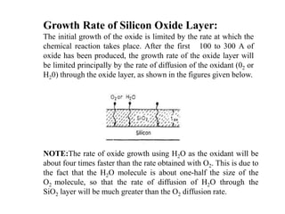
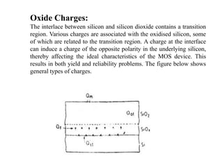
Oxidation Growth Kinetics
In IC Fabrication
Mr. Imran Ahmad
Assistant Professor
JETGI
In Oxidation :
(1)Wafer is exposed to oxygen
(2)Wxygen molecule diffuses into the water
(3)A chemical reaction occurs between oxygen and
silicon
(4)A layer of oxide grows on the water surface
WHY SiO2 ?
The function of a layer of silicon dioxide (SiO2) on a
chip is multipurpose. SiO2 plays an important role in
IC technology because no other semiconductor material
has a native oxide which is able to achieve all the
properties of SiO2.
The role of SiO2 in IC fabrication :
• It is used for surface passivation which is nothing but creating
protective SiO2 layer on the wafer surface. It protects the
junction from moisture and other atmospheric contaminants.
• It serves as an insulator on the water surface. Its high relative
dielectric constant, which enables metal line to pass over the
active silicon regions.
• SiO2 acts as the active gate electrode in MOS device structure.
• It is used to isolate one device from another.
• It provides electrical isolation of multilevel metallization used
in VLSI.
GROWTH OF SILICON OXIDE:
Silicon dioxide (silica) layer is formed on the surface of a silicon
wafer by thermal oxidation at high temperatures in a stream of
oxygen.
Si+02 = SiO2
The rate of oxidation can be significantly increased by adding
water vapour to the oxygen supply to the oxidizing furnace.
Si + 2H2O = SiO2 + 2H2
Growth Rate of Silicon Oxide Layer:
The initial growth of the oxide is limited by the rate at which the
chemical reaction takes place. After the first 100 to 300 A of
oxide has been produced, the growth rate of the oxide layer will
be limited principally by the rate of diffusion of the oxidant (02 or
H20) through the oxide layer, as shown in the figures given below.
NOTE:The rate of oxide growth using H2O as the oxidant will be
about four times faster than the rate obtained with O2. This is due to
the fact that the H2O molecule is about one-half the size of the
O2 molecule, so that the rate of diffusion of H2O through the
SiO2 layer will be much greater than the O2 diffusion rate.
Oxide Charges:
The interlace between silicon and silicon dioxide contains a transition
region. Various charges are associated with the oxidised silicon, some
of which are related to the transition region. A charge at the interface
can induce a charge of the opposite polarity in the underlying silicon,
thereby affecting the ideal characteristics of the MOS device. This
results in both yield and reliability problems. The figure below shows
general types of charges.
(1)Interface-trapped charges
These charges at Si-SiO2 are thought to result from several sources
including structural defects related to the oxidation process, metallic
impurities, or bond breaking processes. The density of these charges is
usually expressed in terms of unit area and energy in the silicon band gap.
(2)Fixed oxide charge
This charge (usually positive) is located in the oxide within approximately
30 A of the Si –SiO2 interface. Fixed oxide charge cannot be charged or
discharged. From a processing point of view, fixed oxide charge is
determined by both temperature and ambient conditions.
(3)Mobile ionic charge
This is attributed to alkali ions such as sodium, potassium, and lithium in
the oxides as well as to negative ions and heavy metals. The alkali ions are
mobile even at room temperature when electric fields are present.
(4)Oxide trapped charge
This charge may be positive or negative, due to holes or electrons trapped
in the bulk of the oxide. This charge, associated with defects in the Si02,
may result from ionizing radiation, avalanche injection.
Effect of Impurities on the Oxidation Rate:
The following impurities affect the oxidation rate
• Water
• Group III and V elements: During thermal oxidation process, an interface
is formed, which separates the silicon from silicon dioxide. As oxidation
proceeds, this interface advances into the silicon. A doping impurity,
which is initially present in the silicon, will redistribute at the interface
until its chemical potential is the same on each side of the interface. This
redistribution may result in an abrupt change in impurity concentration
across the interface. The ratio of the equilibrium concentration of the
impurity, that is, dopant in silicon to that in SiO2 at the interface is called
the equilibrium segregation coefficient.
• Halogen(such as chlorine)
CRITICAL FACTOR IN CONTROLLING THE GROWTH
RATE DURING OXIDATION:
• TEMPRATURE
• THE LENGTH OF EXPOSURE TO OXYGEN
• THE AMOUNT OF MOISTURE
Oxidation Techniques:
Oxydation techniques chosen depend upon the thickness
and oxide properties required
• Dry and wet oxidation
• High pressure oxidation
• Plasma oxidation

Oxidation

  • 1.
    Oxidation Growth Kinetics InIC Fabrication Mr. Imran Ahmad Assistant Professor JETGI
  • 2.
    In Oxidation : (1)Waferis exposed to oxygen (2)Wxygen molecule diffuses into the water (3)A chemical reaction occurs between oxygen and silicon (4)A layer of oxide grows on the water surface WHY SiO2 ? The function of a layer of silicon dioxide (SiO2) on a chip is multipurpose. SiO2 plays an important role in IC technology because no other semiconductor material has a native oxide which is able to achieve all the properties of SiO2.
  • 3.
    The role ofSiO2 in IC fabrication : • It is used for surface passivation which is nothing but creating protective SiO2 layer on the wafer surface. It protects the junction from moisture and other atmospheric contaminants. • It serves as an insulator on the water surface. Its high relative dielectric constant, which enables metal line to pass over the active silicon regions. • SiO2 acts as the active gate electrode in MOS device structure. • It is used to isolate one device from another. • It provides electrical isolation of multilevel metallization used in VLSI.
  • 4.
    GROWTH OF SILICONOXIDE: Silicon dioxide (silica) layer is formed on the surface of a silicon wafer by thermal oxidation at high temperatures in a stream of oxygen. Si+02 = SiO2 The rate of oxidation can be significantly increased by adding water vapour to the oxygen supply to the oxidizing furnace. Si + 2H2O = SiO2 + 2H2
  • 5.
    Growth Rate ofSilicon Oxide Layer: The initial growth of the oxide is limited by the rate at which the chemical reaction takes place. After the first 100 to 300 A of oxide has been produced, the growth rate of the oxide layer will be limited principally by the rate of diffusion of the oxidant (02 or H20) through the oxide layer, as shown in the figures given below. NOTE:The rate of oxide growth using H2O as the oxidant will be about four times faster than the rate obtained with O2. This is due to the fact that the H2O molecule is about one-half the size of the O2 molecule, so that the rate of diffusion of H2O through the SiO2 layer will be much greater than the O2 diffusion rate.
  • 6.
    Oxide Charges: The interlacebetween silicon and silicon dioxide contains a transition region. Various charges are associated with the oxidised silicon, some of which are related to the transition region. A charge at the interface can induce a charge of the opposite polarity in the underlying silicon, thereby affecting the ideal characteristics of the MOS device. This results in both yield and reliability problems. The figure below shows general types of charges.
  • 7.
    (1)Interface-trapped charges These chargesat Si-SiO2 are thought to result from several sources including structural defects related to the oxidation process, metallic impurities, or bond breaking processes. The density of these charges is usually expressed in terms of unit area and energy in the silicon band gap. (2)Fixed oxide charge This charge (usually positive) is located in the oxide within approximately 30 A of the Si –SiO2 interface. Fixed oxide charge cannot be charged or discharged. From a processing point of view, fixed oxide charge is determined by both temperature and ambient conditions. (3)Mobile ionic charge This is attributed to alkali ions such as sodium, potassium, and lithium in the oxides as well as to negative ions and heavy metals. The alkali ions are mobile even at room temperature when electric fields are present. (4)Oxide trapped charge This charge may be positive or negative, due to holes or electrons trapped in the bulk of the oxide. This charge, associated with defects in the Si02, may result from ionizing radiation, avalanche injection.
  • 8.
    Effect of Impuritieson the Oxidation Rate: The following impurities affect the oxidation rate • Water • Group III and V elements: During thermal oxidation process, an interface is formed, which separates the silicon from silicon dioxide. As oxidation proceeds, this interface advances into the silicon. A doping impurity, which is initially present in the silicon, will redistribute at the interface until its chemical potential is the same on each side of the interface. This redistribution may result in an abrupt change in impurity concentration across the interface. The ratio of the equilibrium concentration of the impurity, that is, dopant in silicon to that in SiO2 at the interface is called the equilibrium segregation coefficient. • Halogen(such as chlorine)
  • 9.
    CRITICAL FACTOR INCONTROLLING THE GROWTH RATE DURING OXIDATION: • TEMPRATURE • THE LENGTH OF EXPOSURE TO OXYGEN • THE AMOUNT OF MOISTURE
  • 10.
    Oxidation Techniques: Oxydation techniqueschosen depend upon the thickness and oxide properties required • Dry and wet oxidation • High pressure oxidation • Plasma oxidation