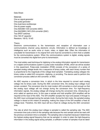
This document describes an experiment to demonstrate pulse-code modulation (PCM) using an analog-to-digital converter (ADC) and a digital-to-analog converter (DAC). The objectives are to encode and decode analog signals using PCM and demonstrate how the sampling rate affects the reproduction of analog signals. The experiment uses an 8-bit ADC to sample an analog input signal and convert it to an 8-bit digital code. The digital output is then converted back to an analog signal using an 8-bit DAC. A low-pass filter is used to smooth the staircase output of the DAC into a representation of the original analog input signal.
This document describes an experiment to demonstrate pulse code modulation (PCM) using an analog-to-digital converter (ADC) and digital-to-analog converter (DAC). The objectives are to encode and decode analog signals using PCM and observe the effects of sampling rate and low-pass filtering. An 8-bit ADC samples an analog input and converts it to an 8-bit digital code. The DAC then reconverts the digital code to an analog output. Low-pass filtering the DAC output smooths the steps to approximate the original analog signal.
1. The experiment demonstrated pulse code modulation (PCM) encoding using an analog-to-digital converter (ADC) and PCM decoding using a digital-to-analog converter (DAC).
2. The sampling frequency determined by the ADC sampling rate generator affected the time between samples on the DAC output. A lower sampling frequency resulted in a longer time between samples and vice versa.
3. The filter cutoff frequency was unaffected by changes to the sampling frequency generator. It was determined solely by the filter capacitor value. With a higher capacitor value, the cutoff frequency decreased.
1) The experiment demonstrated pulse code modulation (PCM) encoding using an analog-to-digital converter (ADC) and decoding using a digital-to-analog converter (DAC).
2) The sampling frequency determined by the pulse generator was measured to be 250 kHz, which was higher than twice the analog input frequency, satisfying the Nyquist criterion.
3) After low-pass filtering the DAC output, the waveform was smoothed into a close approximation of the original analog input signal.
This document describes an experiment to demonstrate pulse code modulation (PCM) using an analog-to-digital converter (ADC) and digital-to-analog converter (DAC). The experiment will encode an analog input signal using an 8-bit ADC and decode it back to an analog output using an 8-bit DAC. The sampling rate of the ADC will determine how well high frequency components of the original analog signal are represented. Passing the DAC's staircase output through a low-pass filter will smooth it into a representation that is closer to the original analog waveform.
This document describes an experiment on pulse code modulation (PCM) using an analog-to-digital converter (ADC) and digital-to-analog converter (DAC). The objectives are to demonstrate PCM encoding and decoding, show how the ADC sampling rate relates to analog signal frequency, and examine the effect of low-pass filtering on the DAC output. The experiment involves using an 8-bit ADC to sample an analog signal and an 8-bit DAC to reconstruct the signal, with a low-pass filter to smooth the DAC output.
The document describes an experiment demonstrating pulse code modulation (PCM) using an analog-to-digital converter (ADC) and digital-to-analog converter (DAC). The experiment showed how the ADC sampling rate must be at least twice the analog signal frequency to avoid aliasing. It also showed that a low-pass filter can smooth the DAC's staircase output into a representation of the original analog signal. The conclusions were that PCM can digitize analog signals for digital communication, with ADC and DAC performing the encoding and decoding, and that the filter output retains the analog input frequency regardless of the sampling rate.
1. The experiment demonstrated pulse-code modulation (PCM) using an analog-to-digital converter (ADC) and digital-to-analog converter (DAC).
2. The DAC output had a staircase-like waveform that was smoothed into an analog signal by a low-pass filter.
3. The sampling frequency determined by the pulse generator affected the time between samples but did not change the cutoff frequency of the filter or the output frequency, which matched the input analog signal frequency.
SIGNAL SPECTRA EXPERIMENT 2 - FINALS (for PULA)Sarah Krystelle
This document describes an experiment conducted on a class B push-pull power amplifier. The objectives were to determine the dc and ac load lines, observe crossover distortion, measure maximum output voltage and power, and calculate efficiency. The circuit diagram and theory of operation for a class B push-pull amplifier are provided. Key steps in the procedure involve using simulations and equipment to analyze the input/output waveforms, dc bias voltages, and performance metrics.
This document describes an experiment on Fourier theory involving the time domain and frequency domain. The objectives are to generate square and triangular waves from Fourier series, examine the difference between time and frequency domain plots, and analyze periodic pulses with different duty cycles in both domains while varying a low-pass filter's cutoff frequency. Procedures generate waves using function generators and measure them on an oscilloscope and spectrum analyzer while eliminating harmonics. The document explains Fourier analysis and how signals can be represented by sine/cosine waves of different frequencies and amplitudes in the frequency domain.
The document summarizes an experiment on characterizing a class A power amplifier. Key steps include:
1) Determining the operating point (Q-point) on the DC load line. 2) Drawing the AC load line and ensuring the Q-point is centered. 3) Measuring the maximum undistorted output voltage and input voltage to calculate voltage gain. The measured gain is compared to theoretical calculations accounting for resistances. Unbypassed emitter resistance reduces gain and stability.
The document summarizes a high-side power switch component. It includes a block diagram showing an N-channel MOSFET power transistor with input, enable, and output pins. It describes the characteristics of the input pin, enable pin, on-state resistance, and turn on/off timing. Simulation results are shown comparing the component's behavior to measurements for various operating conditions.
This document describes an experiment on Fourier theory and its applications in signal processing. The objectives are to: 1) Produce a square wave from sine waves of different frequencies and amplitudes using Fourier theory. 2) Produce a triangular wave similarly using cosine waves. 3) Examine the difference between time domain and frequency domain representations of signals. 4) Analyze periodic pulses with different duty cycles in both domains. 5) Examine the effect of low-pass filtering on pulses as the cutoff frequency varies. The experiment uses function generators, oscilloscopes, spectrum analyzers, and op-amps to generate and analyze signals.
The document discusses generating square and triangular waves using Fourier series of sine and cosine waves. It also examines signals in the time and frequency domains. Key points:
1) A square wave can be produced from a series of sine waves at different frequencies and amplitudes, with the fundamental and odd harmonics present.
2) A triangular wave results from a series of cosine waves, with the fundamental and odd harmonics.
3) Signals can be viewed in the time domain as voltage over time, or in the frequency domain as the amplitude of sine/cosine waves at different frequencies.
This document provides information on the 74F08 integrated circuit, which is a quad two-input AND gate. It includes specifications on propagation delay, supply current, pin configurations, logic diagram, input/output loading, and absolute maximum ratings. The 74F08 is available in commercial and industrial temperature ranges from -40°C to +85°C.
Here are the key steps in the simulation example:
1. Set PWM controller parameters: FOSC, VREF, VP
2. Set output voltage: Rupper, Rlower
3. Select inductor: L for CCM operation
4. Select capacitor: C, ESR for ripple requirements
5. Extract compensator parameters: C1, C2, R1, R2
6. Simulate and verify switching waveforms, efficiency
The example shows designing, simulating, and verifying the operation of the boost converter to meet the given specifications.
SIGNAL SPECTRA EXPERIMENT 1 - FINALS (for CAUAN)Sarah Krystelle
This document describes an experiment conducted on a Class B push-pull power amplifier. The experiment involves determining the operating point on the DC and AC load lines, centering the operating point on the AC load line, measuring the voltage gain, maximum undistorted output power, and efficiency of the amplifier. Objectives of the experiment include locating the operating point, drawing load lines, measuring voltage gain, output power, and efficiency. Components used include a transistor, resistors, capacitors, a power supply, function generator, oscilloscope and multimeter. Calculations are shown for determining load lines, voltage gain, output power and efficiency. Results are recorded for undistorted output voltage and input voltage.
The buck converter simulation example evaluates the switching waveforms and power switch voltages and currents. The specifications include a voltage output of 5V from an input voltage ranging from 7-40V. Inductor and capacitor values are selected to be 330uH and 330uF respectively. Simulation results are obtained for the switching waveforms, power switch voltages and currents using the average models with analysis directives to skip the breakpoints for a 10ms transient simulation.
The document provides information about the 74HC/HCT4020 integrated circuit, which is a 14-stage binary ripple counter. It has 12 parallel outputs, a clock input, and an overriding asynchronous master reset input. The counter advances on the falling edge of the clock input and the master reset input asynchronously clears all counter stages and forces the outputs low. The document includes specifications, pin descriptions, logic diagrams, timing diagrams, and package information.
This document describes wiring diagrams and connector configurations for Alzatex timekeeping products. It includes details on serial connections, remote input wiring, and typical arrangements for connecting Timekeeper units to displays, relay modules, and distribution boxes using standard or crossover phone cords. The document also provides information on jumper settings for bi-directional data transfer and dual channel communication.
This document describes an experiment to characterize active band-pass and band-stop filters. The objectives are to determine the gain-frequency response, center frequency, bandwidth, quality factor, and phase response. For the band-pass filter, the measured and calculated results for center frequency, gain, bandwidth, and quality factor agree to within 5%. For the band-stop filter, the measured and calculated results for center frequency, gain, bandwidth, and quality factor agree to within 1%. The phase response of the band-pass filter shows the output is approximately 180 degrees out of phase with the input at the center frequency.
This document describes the parameters for a power factor correction circuit simulation with the following key details:
1. The circuit includes components like diodes, MOSFETs, resistors, capacitors, and an IC controller.
2. Key parameters include an input AC voltage of 100V at 50Hz, inductors with values of 230uH and a ratio of 1:9.6, and a load current of 0.5A.
3. The circuit aims to provide power factor correction for an AC input voltage using the components and controller.
This document discusses different types of analog-to-digital converters (ADCs). It describes counter type ADCs, successive approximation ADCs, and flash ADCs. It also discusses cascaded ADC architectures that can reduce hardware complexity for high resolution converters. Cascaded designs combine coarse and fine quantization stages to lower component count compared to single-stage flash ADCs. The optimal cascaded design trades off conversion time and hardware cost.
This document describes an experiment involving active band-pass and band-stop filters. The objectives are to determine the gain-frequency response, quality factor, bandwidth, and phase shift of these filters. The experiment uses op-amps, capacitors, and resistors to build a multiple feedback band-pass filter and a two-pole Sallen-Key notch (band-stop) filter. Equations are provided to calculate the center frequency, bandwidth, quality factor, and voltage gain of the filters based on their circuit component values. The procedures involve simulating the filters and measuring their gain-frequency responses to determine these characteristics and compare them to theoretical calculations.
This document describes an experiment on Fourier theory involving the generation of square waves and triangular waves from a series of sine and cosine waves. Key points:
1. Square and triangular waves were generated on an oscilloscope from Fourier series of sine/cosine waves at different frequencies and amplitudes.
2. Measurements showed the fundamental frequency of the generated waves matched the frequency of the individual sine/cosine waves.
3. Removing higher harmonic waves caused the generated waves to become more sinusoidal, demonstrating the role of harmonics in shaping the waveform.
This document describes an experiment on Fourier theory involving the time domain and frequency domain. It explains how square waves and triangular waves can be produced from a series of sine/cosine waves at different frequencies and amplitudes. The experiment uses function generators, an oscilloscope, and spectrum analyzer to generate and observe waveforms in both the time and frequency domains. It also examines how filtering affects periodic pulses with varying duty cycles.
L2 fundamentals of amplitude modulation notesmofaruque1
Modulation involves impressing a low frequency signal onto a higher frequency carrier signal to allow for more efficient transmission. Amplitude modulation (AM) varies the amplitude of the carrier signal based on the amplitude of the intelligence signal. The AM signal consists of the carrier signal plus upper and lower sideband frequencies that carry the modulated information. Power in an AM signal is distributed between the carrier and sidebands, with more power in the sidebands for higher modulation indices up to a maximum of 100% modulation.
This experiment examines amplitude modulation (AM) using a circuit that mathematically multiplies a carrier signal and a modulating signal.
When the modulating signal amplitude is 1 V, the modulation index is 100% based on both calculation and observation of the modulated carrier waveform. The frequency spectrum shows sidebands separated from the carrier by the modulating frequency.
Reducing the modulating signal to 0.5 V yields a modulation index of 50% as expected. Overall the experiment demonstrates the generation of an AM signal and measurement of modulation index from the signal waveform and spectrum.
A product modulator achieves double sideband suppressed carrier (DSB-SC) modulation by multiplying the modulating baseband signal with the carrier signal. Balanced modulators use nonlinear resistances to produce AM modulation and cancel the carrier signal, resulting in a DSB output containing the upper and lower sideband frequencies. A ring modulator works by suppressing the carrier signal when no modulation is present and multiplying the positive and negative halves of the modulating signal by 1 and -1 respectively during modulation.
The document discusses digital baseband modulation and waveform coding techniques. It covers topics like formatting of textual and analog data, pulse code modulation (PCM), quantization, sampling, and delta modulation. Formatting involves character coding using ASCII or EBCDIC. Analog signals are converted to digital form through sampling and quantization. In PCM, an analog signal is sampled, quantized into discrete levels, and encoded into binary digits. Other covered topics include pulse amplitude modulation, pulse width modulation, pulse position modulation, and oversampling.
This document summarizes Chapter 1 from the textbook "Electrical Engineering: Principles and Applications" by Allan R. Hambley. It includes sample exercises and problems from Chapter 1 on topics like charge, current, voltage, power, energy, circuits, and circuit analysis techniques. The chapter introduces fundamental concepts of electrical engineering.
This document discusses amplitude modulation (AM) and covers topics like:
1. Generation of AM signals using double sideband full carrier (DSBFC) modulation.
2. Calculating sideband frequencies and bandwidth for different modulation scenarios.
3. Examining the voltage spectrum and time-domain representation of AM signals.
4. Looking at different AM transmitter and receiver circuit designs including single sideband techniques.
This document discusses an EEE 330 lecture on angle modulation and demodulation. It introduces phase modulation (PM) and frequency modulation (FM), the two main forms of analog angle modulation. PM varies the phase of the carrier linearly with the message signal, while FM varies the frequency of the carrier linearly. The document compares and contrasts PM and FM through examples and discusses narrowband FM, wideband FM, generation and demodulation of FM signals, and practical FM demodulators like the frequency discriminator and phased-locked loop.
Communication - Amplitude Modulation Class 12 Part-1Self-employed
1. The document discusses the basics of communication and amplitude modulation (AM).
2. AM involves varying the amplitude of a carrier wave using an audio signal, resulting in the carrier wave plus two sideband frequencies.
3. The bandwidth required for AM is 2fm, where fm is the highest modulating frequency.
Angle modulation techniques such as frequency modulation (FM) and phase modulation (PM) were introduced. FM varies the carrier frequency according to the message signal, while PM varies the carrier phase. The chapter covered the concepts of instantaneous frequency, bandwidth of angle modulated signals, generation of FM signals through direct and indirect methods, and demodulation of FM signals using discriminators and phase-locked loops. Key advantages of FM over AM include improved noise immunity and resistance to interference at the cost of increased transmission bandwidth.
This document provides an overview of amplitude (linear) modulation techniques. It defines key concepts like modulation, baseband communication, and carrier communication. It then describes various amplitude modulation schemes including AM, DSB-SC, QAM, SSB, and VSB. Implementation and demodulation of these techniques is discussed. The document also covers frequency mixing, superheterodyne receivers, frequency division multiplexing, and carrier acquisition using phase-locked loops. Suggested problems are provided at the end.
This document provides a summary of signal analysis and Fourier series. It begins by defining periodic functions and using examples to determine the period of periodic signals. It then introduces Fourier series and decomposes periodic signals into a sum of sines and cosines. It describes how these sine and cosine functions form an orthogonal basis and can be used to represent any periodic signal. The document also presents the Fourier series in complex exponential form and uses an example of a square wave to illustrate the decomposition. It defines harmonics and discusses how to determine the amplitude and phase of each harmonic component from the Fourier series coefficients.
1) Modulation involves changing characteristics of a high-frequency carrier signal according to an information signal. This allows signal transmission over long distances and multiple signals over the same channel.
2) The main modulation types are amplitude modulation (AM), which changes amplitude; frequency modulation (FM), which changes frequency; and phase modulation (PM), which changes phase.
3) AM is the simplest form and varies the carrier amplitude by the information signal. It has advantages of simplicity but is inefficient in power and bandwidth usage, and susceptible to noise.
This document discusses source coding and channel coding in communication systems. It defines source coding as the process of encoding source data, such as speech or text, into binary format before transmission. Channel coding adds redundancy to encoded data to detect and correct errors during transmission over a noisy communication channel. Common source coding techniques discussed include Huffman coding and Lempel-Ziv algorithms, while channel coding includes block codes and convolution codes. Entropy, mutual information, and other information theory concepts are also introduced.
Frequency modulation and its applicationDarshil Shah
This document discusses frequency modulation (FM) including its definition, modulation index, spectrum characteristics, types of FM modulation, generation of FM using phase modulation, advantages and disadvantages compared to other modulation techniques, and applications of FM such as in radio broadcasting, television sound, and satellite television. FM provides noise immunity and allows adjusting the noise level by changing the frequency deviation. It is widely used for radio but requires more complex transmission and reception equipment than other modulation methods.
This document provides an overview of communication basics and amplitude modulation. It discusses how communication involves transmitting and receiving information, and how modulation translates signals to higher frequencies for long-distance transmission. It then describes various amplitude modulation techniques like AM, DSB, and SSB. Key aspects covered include the AM envelope, frequency spectrum of AM waves, AM modulation indexes, and different AM modulation and demodulation methods.
Solution modern digital-& analog-communications-systems-b-p-lathiFawad Masood
The document repeatedly lists the URL "www.free4vn.org oldroad" over 100 times without any other text or context. It provides no other essential information beyond listing this single URL over and over again.
Digital communication refers to any message passed through digital devices and includes examples like email, texting, fax, videoconferencing. The document discusses the advantages and disadvantages of various digital communication methods, noting that while digital options allow for fast, low-cost communication over large distances, they also come with risks like technical issues, information misuse, and electronic waste. Common digital communication tools covered include email, texting, faxing, teleconferencing, and videoconferencing.
The document presents information on digital to analog conversion (DAC). It discusses the basic concept of DAC, where a digital input is converted to a proportional analog output. It then describes two common types of DAC - the weighted resistor DAC and R-2R ladder DAC. Applications of DACs are also highlighted, such as in digital audio, function generators, and motor controllers. The document provides details on the circuit design and output calculation for both weighted resistor and R-2R ladder DACs. It concludes that the R-2R ladder DAC only requires two resistor values but has slower conversion than the weighted resistor DAC.
A digital to analog converter (DAC) accepts a binary input and produces a proportional analog output signal. A 4-bit DAC has 4 digital inputs representing the 4 bits, with the most significant bit (MSB) as d0 and least significant bit (LSB) as d3. The output voltage v0 is plotted against all possible 16 input combinations. An inverted R/2R ladder DAC uses identical resistors and voltage scaling instead of resistor scaling and a common reference used in a binary-weighted resistor DAC. It uses additional series resistors between nodes for voltage dropping. In a 3-bit R/2R ladder DAC, the binary input 001 connects switches to ground or the inverting op
The Arduino is described as being low cost, easy to use, open source and compatible with multiple platforms. The initial labs focus on basics like blinking an LED and interfacing with the serial port. Later labs introduce communicating with GPS devices and integrating multiple devices. The document outlines various common electronic components that can be interfaced with Arduino like displays, sensors and more. It also defines some common terms used and provides instructions for setting up the Arduino software and board. Contact information is provided for further queries.
1. The document describes the design of a dynamo-speedometer system that uses the rotational power of a bicycle to determine its speed.
2. The system works by converting the AC voltage output of the dynamo into a regulated DC voltage, then measuring the frequency of the AC signal to determine the rotational speed.
3. The speed is determined either by a digital circuit that counts pulses and displays the speed on 7-segment displays, or by a microcontroller that uses timers to measure frequency and displays the speed on an LCD screen.
This document discusses digital to analog converters (DACs). It begins by defining analog and digital signals and what a DAC is. It then describes two common types of DACs: (1) weighted resistor DACs, which use a series of weighted resistors to convert digital codes to analog voltages; and (2) R-2R ladder DACs, which only require two resistor values and are easier to implement accurately. The document concludes by listing some applications of DACs such as digital audio players, signal generators, and motor controllers.
The document discusses analog-to-digital and digital-to-analog converters. It covers key concepts like resolution, bandwidth, energy, sampling, quantization error, and signal-to-noise ratio. Common converter architectures are described, including parallel, R-2R ladder, weighted capacitor, and current-switched DACs as well as flash, pipelined, successive approximation, dual-slope, and sigma-delta ADCs. Tradeoffs between speed, accuracy, and chip area are also addressed.
The document is a presentation on digital to analog conversion (DAC) submitted by three students to their lecturer. It provides an overview of DAC, including definitions and applications. It describes the operation of two common DAC types: weighted resistor DAC and R-2R ladder DAC. For each, it explains how the output analog voltage is determined from the digital input and compares their advantages and disadvantages.
1. Analog to digital converters (ADCs) sample analog signals and convert them into digital words. This allows analog signals from sensors to be processed digitally.
2. The conversion process has two steps - quantization breaks down the analog value into discrete levels, and encoding assigns a digital code to each level. For example, a 3-bit ADC of a 0-10V signal quantizes it into 8 levels separated by 1.25V and encodes each with a 3-bit binary code.
3. There are several types of ADCs including flash, successive approximation, delta-sigma, and dual slope. Flash ADCs are fastest but most expensive, while successive approximation and dual slope ADCs are slower
The document describes a program in BASCOM for an ATMEGA8 microcontroller that uses commands like AT to control sensors and send SMS messages via GSM. It defines variables to store sensor data and SMS messages. The program turns on an LED when sensors are activated or deactivated and sends SMS alerts. It also controls a light that can be turned on or off remotely by SMS commands.
This document describes a simple 0-5V digital voltmeter circuit using an 8051 microcontroller. The circuit uses an ADC0804 analog-to-digital converter to convert the input voltage to a digital value which is then displayed on a 7-segment display. The program controls the ADC to get a digital reading, manipulates the value to display it on the display properly, and multiplexes the display digits by activating the display driver transistors at different times.
Digital to analog converters (DACs) and analog to digital converters (ADCs) allow the conversion between analog and digital signals. DACs take a digital input and output a proportional analog voltage. Common DAC types include binary weighted resistor DACs and R-2R ladder DACs. ADCs take an analog input and output a digital code representing that voltage. Common ADC types are successive approximation ADCs, dual slope integrator ADCs, and counter/staircase ramp ADCs. Data converters are essential for digital signal processing and the interfacing of analog and digital systems.
Prasad Pawaskar describes an analog-to-digital converter circuit using an ADC0808 chip that converts an analog input voltage to an 8-bit digital output without needing a microprocessor. The ADC0808 is an 8-bit analog-to-digital converter with data lines D0 through D7 that works on the principle of successive approximation to continuously convert an input voltage. A row of LEDs is used to display the 8-bit digital output corresponding to the instantaneous analog input value.
Digital voltmeter using 89c51 microcontrollerSaylee joshi
Voltmeter is a voltage measuring instrument.
We can measure the potential difference between any two points in an electrical network using voltmeter.
There are two types of voltmeter as analog voltmeter and digital voltmeter.
Analog voltmeter moves pointer on a scale but it has some limitations like accuracy of few percent of full scale.
Digital voltmeter can display numerical value of voltage on a display by use of analog to digital converter (ADC).
All the data processing and manipulating is in digital form, so it is very essential to use ADC.
We have used ADC0804 analog-to-digital converter IC. The range of input voltage is 0-15V. Here the input voltage should be DC voltage so as to get the steady output on the LCD display.
If you give the AC voltage as an input, it will display continuously running numbers as the nature of AC voltage.
The document discusses different types of analog to digital converters (ADCs). It describes 6 main types - counter/ramp ADC, tracking ADC, successive approximation ADC, flash ADC, delta-sigma ADC, and dual slope integrating ADC. For each type it provides a brief overview of the operating principle and block diagram. It also discusses important ADC specifications and parameters such as resolution, quantization error, dynamic range, signal to noise ratio, aperture delay etc.
Designing Mixed Signal Systems with Noise Reduction Techniques in Mind focused on implementing noise reduction techniques when designing mixed signal systems. The presentation covered sources of noise such as devices, emissions, and traces; techniques to reduce noise like choosing lower noise devices, improving layout, and adding filtering; and applying these techniques across three design revisions to significantly reduce noise. Testing results showed noise levels drop from 44 code widths to just 1 after implementing various noise reduction strategies in a weight sensing application.
The document discusses analog and digital signals, describing analog signals as continuous and digital signals as discrete values separated by fixed time intervals. It then provides explanations of digital-to-analog conversion using voltage dividers or R-2R ladders, and analog-to-digital conversion using flash converters that compare the input to reference voltages or single-slope integration that charges a capacitor until a threshold is reached. Common analog-to-digital converter architectures like flash, single-slope, and successive approximation are also summarized.
This document provides information about analog to digital conversion and digital to analog conversion. It discusses different types of converters including flash ADCs, successive approximation ADCs, dual slope ADCs, R-2R ladder DACs, and weighted resistor DACs. It also covers analog and digital signals, the conversion processes, and applications of ADCs and DACs in areas like data acquisition and fiber optic communication.
The document describes an algorithm for synthesizing a system-level bus from a set of communication channels. The algorithm determines the optimal bus width to balance performance and interconnect cost. It computes the bus rate based on width and delay, and channel rates based on data access patterns and transfer sizes. The bus rate must be greater than or equal to the peak rates of the channels to avoid bottlenecks. The algorithm relates the bus and channel rates to efficiently implement the channels with a single bus.
This document discusses analog to digital and digital to analog signal conversion. It covers:
1) The resolution and accuracy of digitized analog signals depending on the number of bits and voltage span of the analog-to-digital converter.
2) How digital-to-analog converters operate by producing discrete voltage values for each digital code using techniques like binary-weighted resistor DACs and R-2R ladder DACs.
3) How analog-to-digital converters like the 8-bit DAC0800 family work by converting an analog input current to a digital output based on a reference current and voltage.
This document discusses the dual slope analog-to-digital converter (ADC). It begins by defining an ADC and listing common types. It then describes the dual slope ADC in more detail. The dual slope ADC works by integrating an unknown input voltage for a fixed time, then integrating a reference voltage of opposite polarity until the integrator output returns to zero. The digital output is based on the reference voltage, integration times, and clock measurements. The dual slope ADC has advantages like noise reduction but is slower than other ADCs and requires precise external components for high accuracy. Its applications include temperature measurement and digital voltmeters.
SIGNAL SPECTRA EXPERIMENT 2 - FINALS (for CAUAN)Sarah Krystelle
This document describes Experiment #2 on a class B push-pull power amplifier. The objectives are to determine the dc and ac load lines, observe crossover distortion, measure voltage gain, output power, and efficiency. Sample computations are provided for voltage gain, output power, input power, and efficiency. The theory section describes class B push-pull amplifiers and how biasing the transistors slightly above cutoff can eliminate crossover distortion. Procedures are outlined to simulate and measure the amplifier's input, output, voltage gain, power output, and efficiency.
SIGNAL SPECTRA EXPERIMENT 1 - FINALS (for PULA)Sarah Krystelle
The document describes Experiment #1 on a class A power amplifier. It involves determining the operating point (Q-point) on the DC and AC load lines, measuring the voltage gain, maximum undistorted output, and efficiency. The student is to perform steps such as calculating voltages/currents, drawing load lines, measuring gain, and adjusting the emitter resistance to center the Q-point on the AC load line. Objectives include analyzing the amplifier's DC and AC characteristics, measuring linearity and maximum output before clipping occurs.
SIGNAL SPECTRA EXPERIMENT 1 - FINALS (for AGDON)Sarah Krystelle
This experiment analyzed the operation of a class A power amplifier. Key findings include:
1) The initial operating point (Q-point) was not centered on the AC load line, resulting in output clipping.
2) Adjusting the emitter resistance centered the Q-point on the AC load line, eliminating clipping and increasing the maximum undistorted output voltage.
3) A class A amplifier has low efficiency due to conduction over the entire input cycle, but provides the most linear amplification.
SIGNAL SPECTRA EXPERIMENT 1 - FINALS (for ABDON)Sarah Krystelle
The document describes Experiment #1 on a class A power amplifier. Key points:
1. The operating point (Q-point) of the amplifier was initially not centered on the AC load line, causing distortion. Adjusting the emitter resistor centered the Q-point.
2. With the centered Q-point, the maximum undistorted output voltage increased. The expected and measured output voltages matched closely.
3. A class A amplifier has low efficiency due to conduction over the full input cycle, but provides an undistorted output waveform.
SIGNAL SPECTRA EXPERIMENT AMPLITUDE MODULATIONSarah Krystelle
1. The document describes an experiment on amplitude modulation (AM) involving modulating a carrier signal with different modulation indexes and frequencies.
2. Key objectives are to demonstrate AM signals in the time and frequency domains, determine modulation indexes and bandwidths, and compare side frequency levels.
3. Amplitude modulation varies the amplitude of a carrier signal based on an information-carrying modulating signal. This generates sidebands above and below the carrier frequency.
SIGNAL SPECTRA EXPERIMENT AMPLITUDE MODULATION COPY 2Sarah Krystelle
This experiment demonstrates amplitude modulation (AM) using a circuit that multiplies a carrier signal with a modulating signal and adds the results.
1. The experiment showed AM signals in the time and frequency domains for different modulation indexes. In the time domain, the envelope matched the modulating signal.
2. For 100% modulation, the sideband voltages were half the carrier voltage, matching expectations. The bandwidth matched the modulating frequency.
3. Reducing the modulating signal amplitude to 0.5 V resulted in a modulation index near 50%, close to the expected value, demonstrating the circuit can produce AM signals.
This document describes an experiment on amplitude modulation. The objectives are to demonstrate AM in the time and frequency domains, determine modulation index from plots, and examine how modulation index affects sideband levels. The experiment uses a circuit to multiply a carrier and modulating signal, producing an AM carrier viewed on an oscilloscope in the time domain and a spectrum analyzer in the frequency domain. For a modulation index of 1, the sideband voltage is half the carrier voltage as expected. Changing the modulating signal amplitude produces a lower modulation index as seen in the modulated carrier plot.
1. The document describes an experiment on amplitude modulation (AM) that demonstrates AM in the time and frequency domains for different modulation indexes and modulating frequencies.
2. Key objectives are to observe the modulation index, sideband frequencies, bandwidth, and power distribution between the carrier and sidebands for AM signals.
3. The experiment uses a circuit that multiplies a carrier signal with a modulating signal to generate an AM signal, which is then observed on an oscilloscope in the time domain and a spectrum analyzer in the frequency domain.
The document describes an experiment on amplitude modulation (AM). The objectives are to demonstrate AM signals in the time and frequency domains for different modulation indexes and frequencies. Key aspects covered include modulation index, sideband frequencies, bandwidth, and power distribution between the carrier and sidebands. The experiment uses function generators, an oscilloscope, and spectrum analyzer to generate and analyze AM signals.
1. The document describes an experiment on amplitude modulation (AM) that aims to demonstrate AM in the time and frequency domains for different modulation indexes and frequencies.
2. Key objectives are to determine modulation index, side frequency levels, signal bandwidth, and effects of complex modulation.
3. AM involves varying the amplitude of a carrier wave using a modulating signal, generating sidebands above and below the carrier frequency. The bandwidth occupied depends on the modulating signal frequencies.
1) The document describes an experiment on amplitude modulation (AM) involving demonstrating AM signals in the time and frequency domains for different modulation indexes and frequencies.
2) Key aspects of AM are discussed, including how the modulation index is defined and relates to percent modulation. Modulation indexes above 1 cause overmodulation and distortion.
3) AM generates sidebands above and below the carrier frequency by the modulating frequency. The bandwidth occupied depends on the highest modulating frequency components.
This document describes an experiment on amplitude modulation. The objectives are to demonstrate AM in the time and frequency domains for different modulation indexes and frequencies. The experiment uses a circuit to mathematically multiply a carrier signal with a modulating signal. Key findings include:
- For a 5 kHz modulating signal, the modulation index was 100% and sideband frequencies were 5 kHz from the 100 kHz carrier.
- Reducing the modulating signal to 0.5 V reduced the modulation index to 51%, as expected based on the signal amplitudes.
- Sideband voltage levels were half the carrier voltage for 100% modulation, matching theoretical calculations.
This document describes an experiment on amplitude modulation (AM). The objectives are to demonstrate AM in the time and frequency domains, determine modulation index and bandwidth, and examine how sideband power depends on modulation index. The experiment uses a circuit to mathematically multiply a carrier and modulating signal. Measurements are made on an oscilloscope in the time domain and a spectrum analyzer in the frequency domain. Results show the expected relationships between carrier, sideband frequencies and voltages, and how modulation index impacts bandwidth and sideband power. Changing the modulating signal amplitude alters the measured modulation index as expected.
This document discusses Fourier theory and how it can be used to represent non-sinusoidal signals as a combination of sinusoidal waves of different frequencies and amplitudes. It provides examples of how square waves and triangular waves can be produced by adding together sine and cosine waves. The document also discusses the difference between analyzing signals in the time domain versus the frequency domain and how these representations provide different insights. Finally, it discusses how Fourier analysis can be used to understand the bandwidth requirements to transmit digital pulses accurately.
1. The document describes an experiment on Fourier theory and how signals can be represented in both the time domain and frequency domain. Square waves and triangular waves are generated from a series of sine and cosine waves (Fourier series) and plotted in both domains.
2. Low-pass filters are used to remove higher harmonics from signals. This distorts the original waveshape as more harmonics are removed. The bandwidth needed to transmit pulses with minimal distortion depends on the duty cycle.
3. Objectives include learning how square and triangular waves can be produced from Fourier series, comparing time and frequency domain plots, and examining how duty cycle and filtering affect pulses in both domains.
This document discusses Fourier analysis of signals in the time and frequency domains. It explains that any non-sinusoidal periodic signal can be represented as a sum of sinusoidal waves of different frequencies and amplitudes. Signals are normally expressed in the time domain but Fourier theory allows expressing them in the frequency domain. The frequency spectrum reveals the bandwidth needed to transmit the signal with minimal distortion. Fourier analysis is useful for analyzing digital pulses, and the duty cycle of a periodic pulse train affects its frequency spectrum. Sample circuits are provided to generate square and triangular waves using Fourier series approximations.
1. The document describes experiments on representing non-sinusoidal signals as a sum of sinusoidal waves using Fourier analysis and examining signals in both the time and frequency domains.
2. It involves generating square and triangular waves from Fourier series of sine and cosine waves and observing the effects of removing harmonics on the output waveform.
3. The experiments aim to demonstrate the differences between time and frequency domain representations and determine the bandwidth required to transmit periodic pulses with minimal distortion.
This document describes an experiment on Fourier theory involving the time and frequency domains. The objectives are to: 1) Produce a square wave from sine waves of different frequencies and amplitudes using Fourier series; 2) Produce a triangular wave from cosine waves using Fourier series; 3) Examine the difference between time and frequency domain plots; 4) Examine periodic pulses with different duty cycles in both domains; and 5) Examine the effect of low-pass filtering on pulses. Circuits are provided to generate square and triangular waves from Fourier series components for analysis on an oscilloscope and spectrum analyzer.
1. The document describes an experiment on Fourier theory involving the generation of square waves and triangular waves from a series of sine and cosine waves at different frequencies and amplitudes.
2. Key findings include that a square wave can be produced from odd harmonics of a fundamental sine wave, while a triangular wave can be produced from odd harmonic cosine waves. Eliminating harmonics distorts the output wave shape.
3. The time domain shows voltage over time, while the frequency domain shows amplitude by frequency using a Fourier series. Filtering affects the frequency spectrum and output wave shape.
IMPACT Silver is a pure silver zinc producer with over $260 million in revenue since 2008 and a large 100% owned 210km Mexico land package - 2024 catalysts includes new 14% grade zinc Plomosas mine and 20,000m of fully funded exploration drilling.
[To download this presentation, visit:
https://www.oeconsulting.com.sg/training-presentations]
This PowerPoint compilation offers a comprehensive overview of 20 leading innovation management frameworks and methodologies, selected for their broad applicability across various industries and organizational contexts. These frameworks are valuable resources for a wide range of users, including business professionals, educators, and consultants.
Each framework is presented with visually engaging diagrams and templates, ensuring the content is both informative and appealing. While this compilation is thorough, please note that the slides are intended as supplementary resources and may not be sufficient for standalone instructional purposes.
This compilation is ideal for anyone looking to enhance their understanding of innovation management and drive meaningful change within their organization. Whether you aim to improve product development processes, enhance customer experiences, or drive digital transformation, these frameworks offer valuable insights and tools to help you achieve your goals.
INCLUDED FRAMEWORKS/MODELS:
1. Stanford’s Design Thinking
2. IDEO’s Human-Centered Design
3. Strategyzer’s Business Model Innovation
4. Lean Startup Methodology
5. Agile Innovation Framework
6. Doblin’s Ten Types of Innovation
7. McKinsey’s Three Horizons of Growth
8. Customer Journey Map
9. Christensen’s Disruptive Innovation Theory
10. Blue Ocean Strategy
11. Strategyn’s Jobs-To-Be-Done (JTBD) Framework with Job Map
12. Design Sprint Framework
13. The Double Diamond
14. Lean Six Sigma DMAIC
15. TRIZ Problem-Solving Framework
16. Edward de Bono’s Six Thinking Hats
17. Stage-Gate Model
18. Toyota’s Six Steps of Kaizen
19. Microsoft’s Digital Transformation Framework
20. Design for Six Sigma (DFSS)
To download this presentation, visit:
https://www.oeconsulting.com.sg/training-presentations
Best practices for project execution and deliveryCLIVE MINCHIN
A select set of project management best practices to keep your project on-track, on-cost and aligned to scope. Many firms have don't have the necessary skills, diligence, methods and oversight of their projects; this leads to slippage, higher costs and longer timeframes. Often firms have a history of projects that simply failed to move the needle. These best practices will help your firm avoid these pitfalls but they require fortitude to apply.
Call8328958814 satta matka Kalyan result satta guessing➑➌➋➑➒➎➑➑➊➍
Satta Matka Kalyan Main Mumbai Fastest Results
Satta Matka ❋ Sattamatka ❋ New Mumbai Ratan Satta Matka ❋ Fast Matka ❋ Milan Market ❋ Kalyan Matka Results ❋ Satta Game ❋ Matka Game ❋ Satta Matka ❋ Kalyan Satta Matka ❋ Mumbai Main ❋ Online Matka Results ❋ Satta Matka Tips ❋ Milan Chart ❋ Satta Matka Boss❋ New Star Day ❋ Satta King ❋ Live Satta Matka Results ❋ Satta Matka Company ❋ Indian Matka ❋ Satta Matka 143❋ Kalyan Night Matka..
[To download this presentation, visit:
https://www.oeconsulting.com.sg/training-presentations]
This presentation is a curated compilation of PowerPoint diagrams and templates designed to illustrate 20 different digital transformation frameworks and models. These frameworks are based on recent industry trends and best practices, ensuring that the content remains relevant and up-to-date.
Key highlights include Microsoft's Digital Transformation Framework, which focuses on driving innovation and efficiency, and McKinsey's Ten Guiding Principles, which provide strategic insights for successful digital transformation. Additionally, Forrester's framework emphasizes enhancing customer experiences and modernizing IT infrastructure, while IDC's MaturityScape helps assess and develop organizational digital maturity. MIT's framework explores cutting-edge strategies for achieving digital success.
These materials are perfect for enhancing your business or classroom presentations, offering visual aids to supplement your insights. Please note that while comprehensive, these slides are intended as supplementary resources and may not be complete for standalone instructional purposes.
Frameworks/Models included:
Microsoft’s Digital Transformation Framework
McKinsey’s Ten Guiding Principles of Digital Transformation
Forrester’s Digital Transformation Framework
IDC’s Digital Transformation MaturityScape
MIT’s Digital Transformation Framework
Gartner’s Digital Transformation Framework
Accenture’s Digital Strategy & Enterprise Frameworks
Deloitte’s Digital Industrial Transformation Framework
Capgemini’s Digital Transformation Framework
PwC’s Digital Transformation Framework
Cisco’s Digital Transformation Framework
Cognizant’s Digital Transformation Framework
DXC Technology’s Digital Transformation Framework
The BCG Strategy Palette
McKinsey’s Digital Transformation Framework
Digital Transformation Compass
Four Levels of Digital Maturity
Design Thinking Framework
Business Model Canvas
Customer Journey Map
Starting a business is like embarking on an unpredictable adventure. It’s a journey filled with highs and lows, victories and defeats. But what if I told you that those setbacks and failures could be the very stepping stones that lead you to fortune? Let’s explore how resilience, adaptability, and strategic thinking can transform adversity into opportunity.
𝐔𝐧𝐯𝐞𝐢𝐥 𝐭𝐡𝐞 𝐅𝐮𝐭𝐮𝐫𝐞 𝐨𝐟 𝐄𝐧𝐞𝐫𝐠𝐲 𝐄𝐟𝐟𝐢𝐜𝐢𝐞𝐧𝐜𝐲 𝐰𝐢𝐭𝐡 𝐍𝐄𝐖𝐍𝐓𝐈𝐃𝐄’𝐬 𝐋𝐚𝐭𝐞𝐬𝐭 𝐎𝐟𝐟𝐞𝐫𝐢𝐧𝐠𝐬
Explore the details in our newly released product manual, which showcases NEWNTIDE's advanced heat pump technologies. Delve into our energy-efficient and eco-friendly solutions tailored for diverse global markets.
Anny Serafina Love - Letter of Recommendation by Kellen Harkins, MS.AnnySerafinaLove
This letter, written by Kellen Harkins, Course Director at Full Sail University, commends Anny Love's exemplary performance in the Video Sharing Platforms class. It highlights her dedication, willingness to challenge herself, and exceptional skills in production, editing, and marketing across various video platforms like YouTube, TikTok, and Instagram.
Navigating the world of forex trading can be challenging, especially for beginners. To help you make an informed decision, we have comprehensively compared the best forex brokers in India for 2024. This article, reviewed by Top Forex Brokers Review, will cover featured award winners, the best forex brokers, featured offers, the best copy trading platforms, the best forex brokers for beginners, the best MetaTrader brokers, and recently updated reviews. We will focus on FP Markets, Black Bull, EightCap, IC Markets, and Octa.
The Steadfast and Reliable Bull: Taurus Zodiac Signmy Pandit
Explore the steadfast and reliable nature of the Taurus Zodiac Sign. Discover the personality traits, key dates, and horoscope insights that define the determined and practical Taurus, and learn how their grounded nature makes them the anchor of the zodiac.
Industrial Tech SW: Category Renewal and CreationChristian Dahlen
Every industrial revolution has created a new set of categories and a new set of players.
Multiple new technologies have emerged, but Samsara and C3.ai are only two companies which have gone public so far.
Manufacturing startups constitute the largest pipeline share of unicorns and IPO candidates in the SF Bay Area, and software startups dominate in Germany.
Part 2 Deep Dive: Navigating the 2024 Slowdownjeffkluth1
Introduction
The global retail industry has weathered numerous storms, with the financial crisis of 2008 serving as a poignant reminder of the sector's resilience and adaptability. However, as we navigate the complex landscape of 2024, retailers face a unique set of challenges that demand innovative strategies and a fundamental shift in mindset. This white paper contrasts the impact of the 2008 recession on the retail sector with the current headwinds retailers are grappling with, while offering a comprehensive roadmap for success in this new paradigm.
1. NATIONAL COLLEGE OF SCIENCE & TECHNOLOGY
Amafel Bldg. Aguinaldo Highway Dasmariñas City, Cavite
EXPERIMENT NO. 2
Digital Communication of Analog Data Using
Pulse-Code Modulation (PCM)
Lopera, Jericho James L. September 20, 2011
Signal Spectra and Signal Processing/BSECE 41A1 Score:
Engr. Grace Ramones
Instructor
2. Objectives:
Demonstrate PCM encoding using an analog-to-digital converter (ADC).
Demonstrate PCM encoding using an digital-to-analog converter (DAC)
Demonstrate how the ADC sampling rate is related to the analog signal frequency.
Demonstrate the effect of low-pass filtering on the decoder (DAC) output.
4. Data Sheet:
Materials
One ac signal generator
One pulse generator
One dual-trace oscilloscope
One dc power supply
One ADC0801 A/D converter (ADC)
One DAC0808 (1401) D/A converter (DAC)
Two SPDT switches
One 100 nF capacitor
Resistors: 100 Ω, 10 kΩ
Theory
Electronic communications is the transmission and reception of information over a
communications channel using electronic circuits. Information is defined as knowledge or
intelligence such as audio voice or music, video, or digital data. Often the information id
unsuitable for transmission in its original form and must be converted to a form that is suitable
for the communications system. When the communications system is digital, analog signals
must be converted into digital form prior to transmission.
The most widely used technique for digitizing is the analog information signals for transmission
on a digital communications system is pulse-code modulation (PCM), which we will be studied
in this experiment. Pulse-code modulation (PCM) consists of the conversion of a series of
sampled analog voltage levels into a sequence of binary codes, with each binary number that
is proportional to the magnitude of the voltage level sampled. Translating analog voltages into
binary codes is called A/D conversion, digitizing, or encoding. The device used to perform this
conversion process called an A/D converter, or ADC.
An ADC requires a conversion time, in which is the time required to convert each analog
voltage into its binary code. During the ADC conversion time, the analog input voltage must
remain constant. The conversion time for most modern A/D converters is short enough so that
the analog input voltage will not change during the conversion time. For high-frequency
information signals, the analog voltage will change during the conversion time, introducing an
error called an aperture error. In this case a sample and hold amplifier (S/H amplifier) will be
required at the input of the ADC. The S/H amplifier accepts the input and passes it through to
the ADC input unchanged during the sample mode. During the hold mode, the sampled analog
voltage is stored at the instant of sampling, making the output of the S/H amplifier a fixed dc
voltage level. Therefore, the ADC input will be a fixed dc voltage during the ADC conversion
time.
The rate at which the analog input voltage is sampled is called the sampling rate. The ADC
conversion time puts a limit on the sampling rate because the next sample cannot be read until
the previous conversion time is complete. The sampling rate is important because it determines
the highest analog signal frequency that can be sampled. In order to retain the high-frequency
information in the analog signal acting sampled, a sufficient number of samples must be taken
5. so that all of the voltage changes in the waveform are adequately represented. Because a
modern ADC has a very short conversion time, a high sampling rate is possible resulting in
better reproduction of high0frequency analog signals. Nyquist frequency is equal to twice the
highest analog signal frequency component. Although theoretically analog signal can be
sampled at the Nyquist frequency, in practice the sampling rate is usually higher, depending on
the application and other factors such as channel bandwidth and cost limitations.
In a PCM system, the binary codes generated by the ADC are converted into serial pulses and
transmitted over the communications medium, or channel, to the PCM receiver one bit at a
time. At the receiver, the serial pulses are converted back to the original sequence of parallel
binary codes. This sequence of binary codes is reconverted into a series of analog voltage
levels in a D/A converter (DAC), often called a decoder. In a properly designed system, these
analog voltage levels should be close to the analog voltage levels sampled at the transmitter.
Because the sequence of binary codes applied to the DAC input represent a series of dc
voltage levels, the output of the DAC has a staircase (step) characteristic. Therefore, the
resulting DAC output voltage waveshape is only an approximation to the original analog
voltage waveshape at the transmitter. These steps can be smoothed out into an analog voltage
variation by passing the DAC output through a low-pass filter with a cutoff frequency that is
higher than the highest-frequency component in the analog information signal. The low-pass
filter changes the steps into a smooth curve by eliminating many of the harmonic frequency. If
the sampling rate at the transmitter is high enough, the low-pass filter output should be a good
representation of the original analog signal.
In this experiment, pulse code modulation (encoding) and demodulation (decoding) will be
demonstrated using an 8-bit ADC feeding an 8-bit DAC, as shown in Figure 2-1. This ADC will
convert each of the sampled analog voltages into 8-bit binary code as that represent binary
numbers proportional to the magnitude of the sampled analog voltages. The sampling
frequency generator, connected to the start-of conversion (SOC) terminal on the ADC, will start
conversion at the beginning of each sampling pulse. Therefore, the frequency of the sampling
frequency generator will determine the sampling frequency (sampling rate) of the ADC. The 5
volts connected to the VREF+ terminal of the ADC sets the voltage range to 0-5 V. The 5 volts
connected to the output (OE) terminal on the ADC will keep the digital output connected to the
digital bus. The DAC will convert these digital codes back to the sampled analog voltage levels.
This will result in a staircase output, which will follow the original analog voltage variations. The
staircase output of the DAC feeds of a low-pass filter, which will produce a smooth output curve
that should be a close approximation to the original analog input curve. The 5 volts connected
to the + terminal of the DAC sets the voltage range 0-5 V. The values of resistor R and
capacitor C determine the cutoff frequency (fC) of the low-pass filter, which is determined from
the equation
Figure 23–1 Pulse-Code Modulation (PCM)
6. XSC2
G
T
A B C D
S1 VCC
Key = A 5V
U1
Vin D0
S2
D1
V2 D2
D3 Key = B
2 Vpk D4
10kHz
D5
0° Vref+
D6
Vref-
D7
SOC VCC
OE EOC 5V
D0
D1
D2
D3
D4
D5
D6
D7
ADC
V1 Vref+ R1
VDAC8 Output
5V -0V Vref- 100Ω
200kHz
U2
R2
10kΩ C1
100nF
In an actual PCM system, the ADC output would be transmitted to serial format over a
transmission line to the receiver and converted back to parallel format before being applied to
the DAC input. In Figure 23-1, the ADC output is connected to the DAC input by the digital bus
for demonstration purposes only.
PROCEDURE:
Step 1 Open circuit file FIG 23-1. Bring down the oscilloscope enlargement. Make
sure that the following settings are selected. Time base (Scale = 20 µs/Div,
Xpos = 0 Y/T), Ch A(Scale 2 V/Div, Ypos = 0, DC) Ch B (Scale = 2 V/Div,
Ypos = 0, DC), Trigger (Pos edge, Level = 0, Auto). Run the simulation to
completion. (Wait for the simulation to begin). You have plotted the analog
input signal (red) and the DAC output (blue) on the oscilloscope. Measure
the time between samples (TS) on the DAC output curve plot.
TS = 4 µs
Step 2 Calculate the sampling frequency (fS) based on the time between samples
(TS)
fS = 250 kHz
Question: How did the measure sampling frequency compare with the frequency of the
sampling frequency generator?
The sampling time is almost equal, however, the frequencies have a
differrence of 50 kHz.
How did the sampling frequency compare with the analog input frequency? Was it more than
twice the analog input frequency?
It is much higher; in fact, it is 20 times larger than the input frequency. Yes, it
is more than twice the analog input frequency.
How did the sampling frequency compare with the Nyquist frequency?
7. The Nyquist frequency is higher. Nyquist is 6.28 times more than the
sampling frequency.
Step 3 Click the arrow in the circuit window and press the A key to change Switch A to the
sampling generator output. Change the oscilloscope time base to 10 µs/Div. Run
the simulation for one oscilloscope screen display, and then pause the simulation.
You are plotting the sampling generator (red) and the DAC output (blue).
Question: What is the relationship between the sampling generator output and the DAC
staircase output?
Both outputs are both in digital
Step 4 Change the oscilloscope time base scale to 20 µs/Div. Click the arrow in the circuit
window and press the A key to change Switch A to the analog input. Press the B
key to change the Switch B to Filter Output. Bring down the oscilloscope
enlargement and run the simulation to completion. You are plotting the analog input
(red) and the low-pass filter output (blue) on the oscilloscope
Questions: What happened to the DAC output after filtering? Is the filter output waveshape a
close representation of the analog input waveshape?
It became an analog signal that lags the input analog signal. Yes, it is a close
representation of the input waveshape.
Step 5 Calculate the cutoff frequency (fC) of the low-pass filter.
fC = 15.915 kHz
Question: How does the filter cutoff frequency compare with the analog input frequency?
They have difference of approximately 6 kHz.
Step 6 Change the filter capacitor (C) to 20 nF and calculate the new cutoff frequency (f C).
fC = 79.577 kHz
Step 7 Bring down the oscilloscope enlargement and run the simulation to completion
again.
Question: How did the new filter output compare with the previous filter output? Explain.
It is almost the same.
Step 8 Change the filter capacitor (C) back to 100 nF. Change the Switch B back to the
DAC output. Change the frequency of the sampling frequency generator to 100 kHz.
Bring down the oscilloscope enlargement and run the simulation to completion. You
are plotting the analog input (red) and the DAC output (blue) on the oscilloscope
screen. Measure the time between the samples (TS) on the DAC output curve plot
(blue)
TS = 9.5µs
Question: How does the time between the samples in Step 8 compare with the time between
the samples in Step 1?
The time between the samples in Step 8 doubles.
Step 9 Calculate the new sampling frequency (fS) based on the time between the samples
(TS) in Step 8?
fS=105.26Hz
Question: How does the new sampling frequency compare with the analog input frequency?
The sampling frequency is much higher than the input frequency. It is 10 times the
input frequency.
8. Step 10 Click the arrow in the circuit window and change the Switch B to the filter output.
Bring down the oscilloscope enlargement and run the simulation again.
Question: How does the curve plot in Step 10 compare with the curve plot in Step 4 at the
higher sampling frequency? Is the curve as smooth as in Step 4? Explain why.
Yes, they are the same. It is as smooth as in Step 4. Nothing changed. It does not
affect the filter.
Step 11 Change the frequency of the sampling frequency generator to 50 kHz and change
Switch B back to the DAC output. Bring down the oscilloscope enlargement and run
the simulation to completion. Measure the time between samples (T S) on the DAC
output curve plot (blue).
TS = 19µs
Question: How does the time between samples in Step 11 compare with the time between the
samples in Step 8?
The sampling time doubles.
Step 12 Calculate the new sampling frequency (fS) based on the time between samples (TS)
in Step 11.
fS=52.631 kHz
Question: How does the new sampling frequency compare with the analog input frequency?
The new sampling frequency is 5 times the analog input.
Step 13 Click the arrow in the circuit window and change the Switch B to the filter output.
Bring down the oscilloscope enlargement and run the simulation to completion
again.
Question: How does the curve plot in Step 13 compare with the curve plot in Step 10 at the
higher sampling frequency? Is the curve as smooth as in Step 10? Explain why.
Yes, nothing changed. The frequency of the sampling generator does not affect the
filter.
Step 14 Calculate the frequency of the filter output (f) based on the period for one cycle (T).
T=10kHz
Question: How does the frequency of the filter output compare with the frequency of the analog
input? Was this expected based on the sampling frequency? Explain why.
It is the same. Yes, it is expected.
Step 15 Change the frequency of the sampling frequency generator to 15 kHz and change
Switch B back to the DAC output. Bring down the oscilloscope enlargement and run
the simulation to completion. Measure the time between samples (TS) on the DAC
output curve plot (blue)
TS = 66.5µs
Question: How does the time between samples in Step 15 compare with the time between
samples in Step 11?
It is 3.5 times higher than the time in Step 11.
Step 16 Calculate the new sampling frequency (fS) based on the time between samples (TS)
in Step 15.
fS=15.037 kHz
Question: How does the new sampling frequency compare with the analog input frequency?
It is 5 kHz greater than the analog input frequency.
How does the new sampling frequency compare with the Nyquist frequency?
9. It is much lesser than the Nyquist frequency.
Step 17 Click the arrow in the circuit window and change the Switch B to the filter output.
Bring down the oscilloscope enlargement and run the simulation to completion
again.
Question: How does the curve plot in Step 17 compare with the curve plot in Step 13 at the
higher sampling frequency?
They are the same.
Step 18 Calculate the frequency of the filter output (f) based on the time period for one cycle
(T).
f=10kHz
Question: How does the frequency of the filter output compare with the frequency of the analog
input? Was this expected based on the sampling frequency?
They are the same. Yes, it should be the same for this sampling frequency.
10. CONCLUSION:
Based on the input and the output displayed by the oscilloscope, I conclude that the input
analog signal can be converted into digital through PCM. An ADC is use for PCM encoding while
DAC is use for PCM decoding. The staircase signal is the DAC output and its frequency is
generated by the signal frequency generator connected to the ADC. The sampling time is inversely
proportional to the sampling frequency. Add to that, the filter output is analog like the input analog
signal. Also, the frequency of the filter output is the same as the input analog signal. The cutoff
frequency is inversely proportional to the capacitor, as the capacitor increases, the cutoff
frequency decreases. Lastly, the frequency of the sampling signal is much lesser than the Nyquist
frequency.