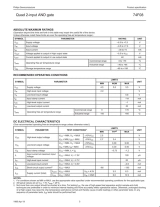
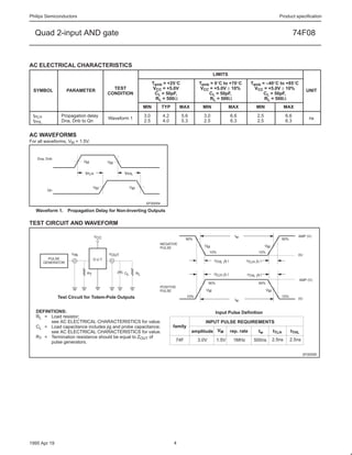
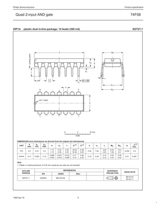
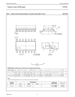
INTEGRATED CIRCUITS


   74F08
   Quad two-input AND gate

Product specification                         1995 Apr 19
IC15 Data Handbook


Philips Semiconductors
Philips Semiconductors                                                                                                      Product specification


  Quad 2-input AND gate                                                                                                                    74F08


• 74F08 Available for industrial range (–40°C to +85°C)                       PIN CONFIGURATION

                                                                                                  D0a    1         14      VCC
   TYPE                TYPICAL                            TYPICAL                                 D0b    2         13      D3b
                     PROPAGATION                      SUPPLY CURRENT
                        DELAY                             (TOTAL)                                  Q0    3         12      D3a

                                                                                                  D1a    4         11      Q3
   74F08                 4.1ns                                  7.1mA
                                                                                                  D1b    5         10      D2b

                                                                                                   Q1    6             9   D2a

                                                                                                  GND    7             8   Q2

                                                                                                                   SF00038


ORDERING INFORMATION
                                          COMMERCIAL RANGE                             INDUSTRIAL RANGE
    DESCRIPTION                                                                                                                      PKG DWG #
                                   VCC = 5.0V ±10%, Tamb = 0°C to +70°C       VCC = 5.0V ±10%, Tamb = –40°C to +85°C
   14-pin plastic DIP                                N74F08N                                 I74F08N                                     SOT27-1
   14-pin plastic SO                                 N74F08D                                 I74F08D                                     SOT108-1


INPUT AND OUTPUT LOADING AND FAN-OUT TABLE
            PINS                                      DESCRIPTION                    74F (U.L.) HIGH/LOW          LOAD VALUE HIGH/LOW
         Dna, Dnb                  Data inputs                                              1.0/1.0                         20µA/0.6mA
                Qn                 Data output                                              50/33                          1.0mA/20mA
NOTE: One (1.0) FAST unit load is defined as: 20µA in the High state and 0.6mA in the Low state.

LOGIC DIAGRAM                                                                 FUNCTION TABLE
                                    1                                                     INPUTS                            OUTPUT
                         D0a                          3
                         D0b        2                      Q0
                                                                                    Dna                 Dnb                      Qn
                                    4
                         D1a                          6                              L                   L                           L
                         D1b        5                      Q1
                                                                                     L                  H                            L
                                    9
                         D2a                          8
                         D2b       10                      Q2                        H                   L                           L
                                   12                 11
                                                                                   H                 H                               H
 VCC = Pin 14            D3a                               Q3
 GND = Pin 7             D3b       13                                         NOTES:
                                                                              H = High voltage level
                                                     SF00052
                                                                              L = Low voltage level

LOGIC SYMBOL                                                                  LOGIC SYMBOL (IEEE/IEC)
                         1     2    4   5   9   10 12 13
                                                                                             1                &
                                                                                                                                 3
                                                                                             2


                        D0a D0bD1a D1b D2a D2b D3a D3b
                                                                                             4
                                                                                                                                 6
                                                                                             5

                                   Q0 Q1 Q2 Q3
                                                                                             9
                                                                                                                                 8
                                                                                             10
  VCC = Pin 14
  GND = Pin 7                       3   6   8   11
                                                                                             12
                                                     SF00040                                                                     11
                                                                                             13


                                                                                                                           SF00053


 1995 Apr 19                                                              2                                                           853–0328 15145
Philips Semiconductors                                                                                                           Product specification


   Quad 2-input AND gate                                                                                                               74F08


ABSOLUTE MAXIMUM RATINGS
(Operation beyond the limits set forth in this table may impair the useful life of the device.
Unless otherwise noted these limits are over the operating free-air temperature range.)
 SYMBOL                                               PARAMETER                                                      RATING                 UNIT
 VCC          Supply voltage                                                                                        –0.5 to +7.0              V
 VIN          Input voltage                                                                                         –0.5 to +7.0              V
 IIN          Input current                                                                                          –30 to +5               mA
 VOUT         Voltage applied to output in High output state                                                        –0.5 to VCC               V
 IOUT         Current applied to output in Low output state                                                             40                   mA
                                                                                         Commercial range            0 to +70                °C
 Tamb         Operating free-air temperature range
                        free air
                                                                                         Industrial range           –40 to +85               °C
 Tstg         Storage temperature range                                                                             –65 to +150              °C


RECOMMENDED OPERATING CONDITIONS
                                                                                                            LIMITS
 SYMBOL                                          PARAMETER                                                                                 UNIT
                                                                                                    MIN     NOM              MAX
 VCC           Supply voltage                                                                        4.5     5.0             5.5             V
 VIh           High-level input voltage                                                              2.0                                     V
 VIL           Low-level input voltage                                                                                       0.8             V
 IIK           Input clamp current                                                                                           –18            mA
 IOH           High-level output current                                                                                      –1            mA
 IOL           Low-level output current                                                                                       20            mA
                                                                      Commercial range                0                      +70             °C
 Tamb
    b          O erating
               Operating free-air tem erature range
                                  temperature
                                                                      Industrial range              –40                      +85             °C


DC ELECTRICAL CHARACTERISTICS
(Over recommended operating free-air temperature range unless otherwise noted.)
                                                                                                            LIMITS
  SYMBOL                 PARAMETER                           TEST CONDITIONS1                                                              UNIT
                                                                                                    MIN     TYP2             MAX
                                                    VCC = MIN, VIL = MAX         ±10%VCC            2.5                                      V
  VO
   OH          High level output voltage
               High-level
                                                    VIH = MIN, IOH = MAX          ±5%VCC            2.7      3.4                             V
                                                    VCC = MIN, VIL = MAX         ±10%VCC                     0.30            0.50            V
  VO
   OL          Low-level
               Low level output voltage
                                                    VIH = MIN, IOl = MAX          ±5%VCC                     0.30            0.50            V
  VIK          Input clamp voltage                  VCC = MIN, II = IIK                                     –0.73            –1.2            V
               Input current at maximum input
  II                                                VCC = MAX, VI = 7.0V                                                     100            µA
               voltage
  IIH          High-level input current             VCC = MAX, VI = 2.7V                                                     20             µA
  IIL          Low-level input current              VCC = MAX, VI = 0.5V                                                     –0.6           mA
  IOS          Short-circuit output   current3      VCC = MAX                                       –60                      –150           mA
                                             ICCH   VCC = MAX                    VIN = 4.5V                  5.5             8.3            mA
  ICC          Supply current (total)
                                           ICCL VCC = MAX                    VIN = GND                       8.6         12.9          mA
NOTES:
1. For conditions shown as MIN or MAX, use the appropriate value specified under recommended operating conditions for the applicable type.
2. All typical values are at VCC = 5V, Tamb = 25°C.
3. Not more than one output should be shorted at a time. For testing IOS, the use of high-speed test apparatus and/or sample-and-hold
   techniques are preferable in order to minimize internal heating and more accurately reflect operational values. Otherwise, prolonged shorting
   of a High output may raise the chip temperature well above normal and thereby cause invalid readings in other parameter tests. In any
   sequence of parameter tests, IOS tests should be performed last.


1995 Apr 19                                                                3
Philips Semiconductors                                                                                                                               Product specification


  Quad 2-input AND gate                                                                                                                                         74F08


AC ELECTRICAL CHARACTERISTICS
                                                                                                         LIMITS
                                                                      Tamb = +25°C               Tamb = 0°C to +70°C               Tamb = –40°C to +85°C
 SYMBOL             PARAMETER               TEST                       VCC = +5.0V                VCC = +5.0V ± 10%                  VCC = +5.0V ± 10%                  UNIT
                                          CONDITION                     CL = 50pF,                   CL = 50pF,                          CL = 50pF,
                                                                        RL = 500Ω                     RL = 500Ω                          RL = 500Ω
                                                                MIN        TYP        MAX          MIN               MAX             MIN                  MAX
 tPLH          Propagation delay                                3.0         4.2       5.6          3.0                 6.6            2.5                 6.6
                                          Waveform 1                                                                                                                      ns
 tPHL          Dna, Dnb to Qn                                   2.5         4.0       5.3          2.5                 6.3            2.5                 6.3


AC WAVEFORMS
For all waveforms, VM = 1.5V.


   Dna, Dnb
                           VM             VM


                           tPLH                  tPHL


                                 VM                   VM
         Qn


                                                                 SF00054

   Waveform 1. Propagation Delay for Non-Inverting Outputs

TEST CIRCUIT AND WAVEFORM

                                  VCC                                                                                    tw                                       AMP (V)
                                                                                         90%                                                             90%
                                                                           NEGATIVE
                                                                                                   VM                                       VM
                                                                           PULSE
                                                                                                        10%                            10%
                     VIN                  VOUT                                                                                                                    0V
          PULSE                  D.U.T.
        GENERATOR                                                                                         tTHL (tf )           tTLH (tr )


                            RT                   CL        RL                                             tTLH (tr )           tTHL (tf )
                                                                                                                                                                   AMP (V)
                                                                                                        90%                            90%
                                                                           POSITIVE
                                                                           PULSE                    VM                                       VM

              Test Circuit for Totem-Pole Outputs                                          10%                                                           10%
                                                                                                                         tw                                       0V


   DEFINITIONS:                                                                                               Input Pulse Definition
   RL = Load resistor;
         see AC ELECTRICAL CHARACTERISTICS for value.                                               INPUT PULSE REQUIREMENTS
   CL = Load capacitance includes jig and probe capacitance;                      family
         see AC ELECTRICAL CHARACTERISTICS for value.                                       amplitude VM               rep. rate       tw         tTLH         tTHL
   RT = Termination resistance should be equal to ZOUT of
                                                                                   74F           3.0V         1.5V      1MHz        500ns         2.5ns        2.5ns
         pulse generators.

                                                                                                                                                                       SF00006


1995 Apr 19                                                                       4
Philips Semiconductors                                    Product specification


  Quad 2-input AND gate                                         74F08


DIP14: plastic dual in-line package; 14 leads (300 mil)           SOT27-1


1995 Apr 19                                          5
Philips Semiconductors                                             Product specification


  Quad 2-input AND gate                                                  74F08


SO14: plastic small outline package; 14 leads; body width 3.9 mm          SOT108-1


1995 Apr 19                                       6
Philips Semiconductors            Product specification


  Quad 2-input AND gate                 74F08


                          NOTES


1995 Apr 19                 7
Philips Semiconductors                                                                                                            Product specification


  Quad 2-input AND gate                                                                                                                  74F08


Data sheet status
Data sheet          Product             Definition [1]
status              status

Objective           Development         This data sheet contains the design target or goal specifications for product development.
specification                           Specification may change in any manner without notice.

Preliminary         Qualification       This data sheet contains preliminary data, and supplementary data will be published at a later date.
specification                           Philips Semiconductors reserves the right to make chages at any time without notice in order to
                                        improve design and supply the best possible product.
Product             Production          This data sheet contains final specifications. Philips Semiconductors reserves the right to make
specification                           changes at any time without notice in order to improve design and supply the best possible product.

[1] Please consult the most recently issued datasheet before initiating or completing a design.

Definitions
Short-form specification — The data in a short-form specification is extracted from a full data sheet with the same type number and title. For
detailed information see the relevant data sheet or data handbook.
Limiting values definition — Limiting values given are in accordance with the Absolute Maximum Rating System (IEC 134). Stress above one
or more of the limiting values may cause permanent damage to the device. These are stress ratings only and operation of the device at these or
at any other conditions above those given in the Characteristics sections of the specification is not implied. Exposure to limiting values for extended
periods may affect device reliability.
Application information — Applications that are described herein for any of these products are for illustrative purposes only. Philips
Semiconductors make no representation or warranty that such applications will be suitable for the specified use without further testing or
modification.

Disclaimers
Life support — These products are not designed for use in life support appliances, devices or systems where malfunction of these products can
reasonably be expected to result in personal injury. Philips Semiconductors customers using or selling these products for use in such applications
do so at their own risk and agree to fully indemnify Philips Semiconductors for any damages resulting from such application.
Right to make changes — Philips Semiconductors reserves the right to make changes, without notice, in the products, including circuits, standard
cells, and/or software, described or contained herein in order to improve design and/or performance. Philips Semiconductors assumes no
responsibility or liability for the use of any of these products, conveys no license or title under any patent, copyright, or mask work right to these
products, and makes no representations or warranties that these products are free from patent, copyright, or mask work right infringement, unless
otherwise specified.

 Philips Semiconductors                                                            © Copyright Philips Electronics North America Corporation 1998
 811 East Arques Avenue                                                                                        All rights reserved. Printed in U.S.A.
 P.O. Box 3409
 Sunnyvale, California 94088–3409                                                     print code                                    Date of release: 10-98
 Telephone 800-234-7381
                                                                                      Document order number:                             9397-750-05055


Philips
Semiconductors
yyyy mmm dd                                                               8

74 f08

  • 1.
    INTEGRATED CIRCUITS 74F08 Quad two-input AND gate Product specification 1995 Apr 19 IC15 Data Handbook Philips Semiconductors
  • 2.
    Philips Semiconductors Product specification Quad 2-input AND gate 74F08 • 74F08 Available for industrial range (–40°C to +85°C) PIN CONFIGURATION D0a 1 14 VCC TYPE TYPICAL TYPICAL D0b 2 13 D3b PROPAGATION SUPPLY CURRENT DELAY (TOTAL) Q0 3 12 D3a D1a 4 11 Q3 74F08 4.1ns 7.1mA D1b 5 10 D2b Q1 6 9 D2a GND 7 8 Q2 SF00038 ORDERING INFORMATION COMMERCIAL RANGE INDUSTRIAL RANGE DESCRIPTION PKG DWG # VCC = 5.0V ±10%, Tamb = 0°C to +70°C VCC = 5.0V ±10%, Tamb = –40°C to +85°C 14-pin plastic DIP N74F08N I74F08N SOT27-1 14-pin plastic SO N74F08D I74F08D SOT108-1 INPUT AND OUTPUT LOADING AND FAN-OUT TABLE PINS DESCRIPTION 74F (U.L.) HIGH/LOW LOAD VALUE HIGH/LOW Dna, Dnb Data inputs 1.0/1.0 20µA/0.6mA Qn Data output 50/33 1.0mA/20mA NOTE: One (1.0) FAST unit load is defined as: 20µA in the High state and 0.6mA in the Low state. LOGIC DIAGRAM FUNCTION TABLE 1 INPUTS OUTPUT D0a 3 D0b 2 Q0 Dna Dnb Qn 4 D1a 6 L L L D1b 5 Q1 L H L 9 D2a 8 D2b 10 Q2 H L L 12 11 H H H VCC = Pin 14 D3a Q3 GND = Pin 7 D3b 13 NOTES: H = High voltage level SF00052 L = Low voltage level LOGIC SYMBOL LOGIC SYMBOL (IEEE/IEC) 1 2 4 5 9 10 12 13 1 & 3 2 D0a D0bD1a D1b D2a D2b D3a D3b 4 6 5 Q0 Q1 Q2 Q3 9 8 10 VCC = Pin 14 GND = Pin 7 3 6 8 11 12 SF00040 11 13 SF00053 1995 Apr 19 2 853–0328 15145
  • 3.
    Philips Semiconductors Product specification Quad 2-input AND gate 74F08 ABSOLUTE MAXIMUM RATINGS (Operation beyond the limits set forth in this table may impair the useful life of the device. Unless otherwise noted these limits are over the operating free-air temperature range.) SYMBOL PARAMETER RATING UNIT VCC Supply voltage –0.5 to +7.0 V VIN Input voltage –0.5 to +7.0 V IIN Input current –30 to +5 mA VOUT Voltage applied to output in High output state –0.5 to VCC V IOUT Current applied to output in Low output state 40 mA Commercial range 0 to +70 °C Tamb Operating free-air temperature range free air Industrial range –40 to +85 °C Tstg Storage temperature range –65 to +150 °C RECOMMENDED OPERATING CONDITIONS LIMITS SYMBOL PARAMETER UNIT MIN NOM MAX VCC Supply voltage 4.5 5.0 5.5 V VIh High-level input voltage 2.0 V VIL Low-level input voltage 0.8 V IIK Input clamp current –18 mA IOH High-level output current –1 mA IOL Low-level output current 20 mA Commercial range 0 +70 °C Tamb b O erating Operating free-air tem erature range temperature Industrial range –40 +85 °C DC ELECTRICAL CHARACTERISTICS (Over recommended operating free-air temperature range unless otherwise noted.) LIMITS SYMBOL PARAMETER TEST CONDITIONS1 UNIT MIN TYP2 MAX VCC = MIN, VIL = MAX ±10%VCC 2.5 V VO OH High level output voltage High-level VIH = MIN, IOH = MAX ±5%VCC 2.7 3.4 V VCC = MIN, VIL = MAX ±10%VCC 0.30 0.50 V VO OL Low-level Low level output voltage VIH = MIN, IOl = MAX ±5%VCC 0.30 0.50 V VIK Input clamp voltage VCC = MIN, II = IIK –0.73 –1.2 V Input current at maximum input II VCC = MAX, VI = 7.0V 100 µA voltage IIH High-level input current VCC = MAX, VI = 2.7V 20 µA IIL Low-level input current VCC = MAX, VI = 0.5V –0.6 mA IOS Short-circuit output current3 VCC = MAX –60 –150 mA ICCH VCC = MAX VIN = 4.5V 5.5 8.3 mA ICC Supply current (total) ICCL VCC = MAX VIN = GND 8.6 12.9 mA NOTES: 1. For conditions shown as MIN or MAX, use the appropriate value specified under recommended operating conditions for the applicable type. 2. All typical values are at VCC = 5V, Tamb = 25°C. 3. Not more than one output should be shorted at a time. For testing IOS, the use of high-speed test apparatus and/or sample-and-hold techniques are preferable in order to minimize internal heating and more accurately reflect operational values. Otherwise, prolonged shorting of a High output may raise the chip temperature well above normal and thereby cause invalid readings in other parameter tests. In any sequence of parameter tests, IOS tests should be performed last. 1995 Apr 19 3
  • 4.
    Philips Semiconductors Product specification Quad 2-input AND gate 74F08 AC ELECTRICAL CHARACTERISTICS LIMITS Tamb = +25°C Tamb = 0°C to +70°C Tamb = –40°C to +85°C SYMBOL PARAMETER TEST VCC = +5.0V VCC = +5.0V ± 10% VCC = +5.0V ± 10% UNIT CONDITION CL = 50pF, CL = 50pF, CL = 50pF, RL = 500Ω RL = 500Ω RL = 500Ω MIN TYP MAX MIN MAX MIN MAX tPLH Propagation delay 3.0 4.2 5.6 3.0 6.6 2.5 6.6 Waveform 1 ns tPHL Dna, Dnb to Qn 2.5 4.0 5.3 2.5 6.3 2.5 6.3 AC WAVEFORMS For all waveforms, VM = 1.5V. Dna, Dnb VM VM tPLH tPHL VM VM Qn SF00054 Waveform 1. Propagation Delay for Non-Inverting Outputs TEST CIRCUIT AND WAVEFORM VCC tw AMP (V) 90% 90% NEGATIVE VM VM PULSE 10% 10% VIN VOUT 0V PULSE D.U.T. GENERATOR tTHL (tf ) tTLH (tr ) RT CL RL tTLH (tr ) tTHL (tf ) AMP (V) 90% 90% POSITIVE PULSE VM VM Test Circuit for Totem-Pole Outputs 10% 10% tw 0V DEFINITIONS: Input Pulse Definition RL = Load resistor; see AC ELECTRICAL CHARACTERISTICS for value. INPUT PULSE REQUIREMENTS CL = Load capacitance includes jig and probe capacitance; family see AC ELECTRICAL CHARACTERISTICS for value. amplitude VM rep. rate tw tTLH tTHL RT = Termination resistance should be equal to ZOUT of 74F 3.0V 1.5V 1MHz 500ns 2.5ns 2.5ns pulse generators. SF00006 1995 Apr 19 4
  • 5.
    Philips Semiconductors Product specification Quad 2-input AND gate 74F08 DIP14: plastic dual in-line package; 14 leads (300 mil) SOT27-1 1995 Apr 19 5
  • 6.
    Philips Semiconductors Product specification Quad 2-input AND gate 74F08 SO14: plastic small outline package; 14 leads; body width 3.9 mm SOT108-1 1995 Apr 19 6
  • 7.
    Philips Semiconductors Product specification Quad 2-input AND gate 74F08 NOTES 1995 Apr 19 7
  • 8.
    Philips Semiconductors Product specification Quad 2-input AND gate 74F08 Data sheet status Data sheet Product Definition [1] status status Objective Development This data sheet contains the design target or goal specifications for product development. specification Specification may change in any manner without notice. Preliminary Qualification This data sheet contains preliminary data, and supplementary data will be published at a later date. specification Philips Semiconductors reserves the right to make chages at any time without notice in order to improve design and supply the best possible product. Product Production This data sheet contains final specifications. Philips Semiconductors reserves the right to make specification changes at any time without notice in order to improve design and supply the best possible product. [1] Please consult the most recently issued datasheet before initiating or completing a design. Definitions Short-form specification — The data in a short-form specification is extracted from a full data sheet with the same type number and title. For detailed information see the relevant data sheet or data handbook. Limiting values definition — Limiting values given are in accordance with the Absolute Maximum Rating System (IEC 134). Stress above one or more of the limiting values may cause permanent damage to the device. These are stress ratings only and operation of the device at these or at any other conditions above those given in the Characteristics sections of the specification is not implied. Exposure to limiting values for extended periods may affect device reliability. Application information — Applications that are described herein for any of these products are for illustrative purposes only. Philips Semiconductors make no representation or warranty that such applications will be suitable for the specified use without further testing or modification. Disclaimers Life support — These products are not designed for use in life support appliances, devices or systems where malfunction of these products can reasonably be expected to result in personal injury. Philips Semiconductors customers using or selling these products for use in such applications do so at their own risk and agree to fully indemnify Philips Semiconductors for any damages resulting from such application. Right to make changes — Philips Semiconductors reserves the right to make changes, without notice, in the products, including circuits, standard cells, and/or software, described or contained herein in order to improve design and/or performance. Philips Semiconductors assumes no responsibility or liability for the use of any of these products, conveys no license or title under any patent, copyright, or mask work right to these products, and makes no representations or warranties that these products are free from patent, copyright, or mask work right infringement, unless otherwise specified. Philips Semiconductors © Copyright Philips Electronics North America Corporation 1998 811 East Arques Avenue All rights reserved. Printed in U.S.A. P.O. Box 3409 Sunnyvale, California 94088–3409 print code Date of release: 10-98 Telephone 800-234-7381 Document order number: 9397-750-05055 Philips Semiconductors yyyy mmm dd 8