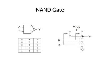
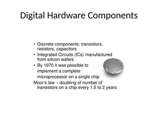
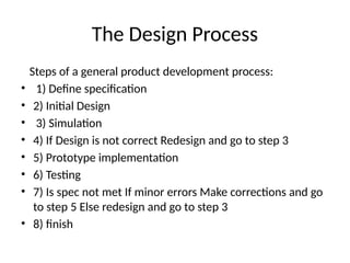
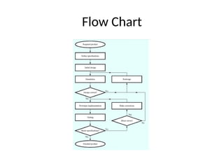
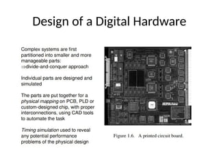
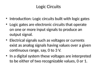
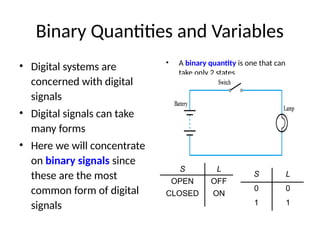
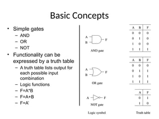
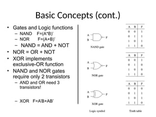
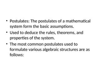
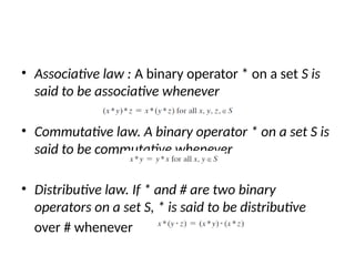
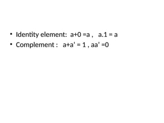
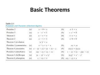
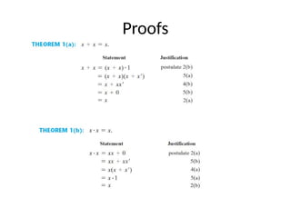
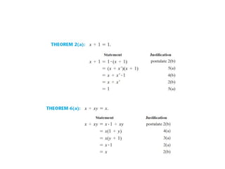
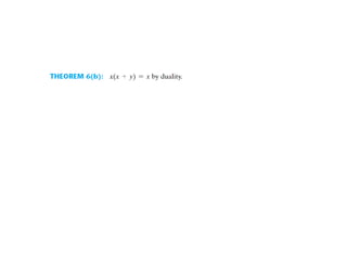
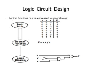
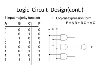
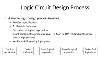
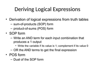
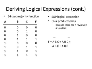
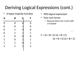
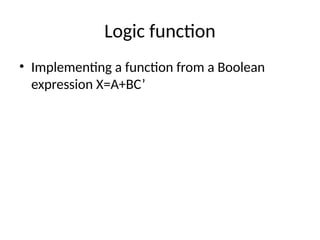
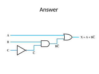
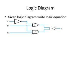
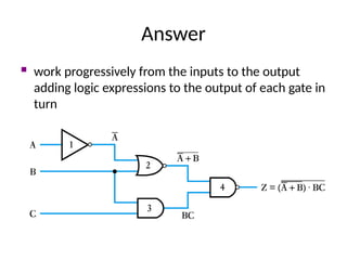
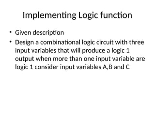
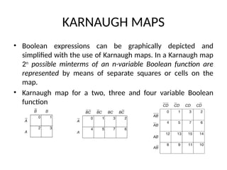
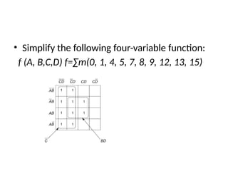
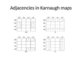
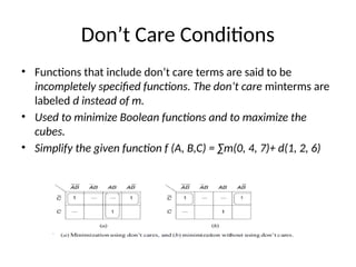
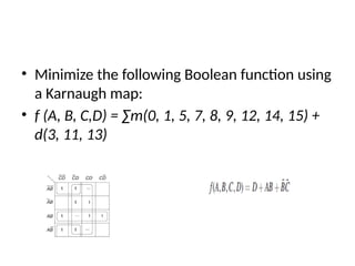
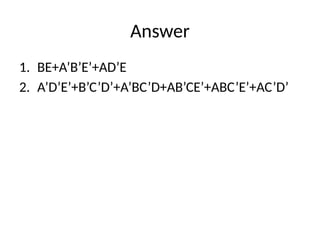
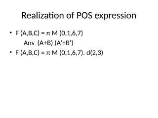
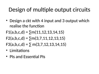
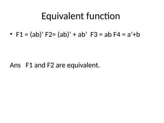
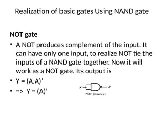
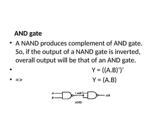
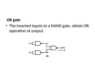
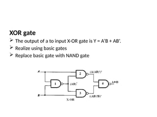
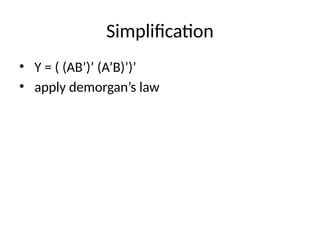
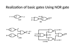
DIGITAL ELECTRONICS
BE IT III Semester
Dr. M Mohammed Sabir Hussain
Sabir.mj@gmail.com
9849217818
Syllabus
UNIT – I
• Design Concepts: Digital Hardware, Design
process, Design of digital hardware.
Introduction to logic circuits – Variables and
functions, Logic gates and networks. Boolean
algebra, Synthesis using gates, Design
examples. Optimized implementation of logic
functions using K-Map
Course Outcomes
• At the end of this course the students will be able to
• Understand the deign process of digital hardware, use Boolean algebra to
minimize the logical expressions and optimize the implementation of
logical functions.
• Understand the number representation and design combinational circuits
like adders, MUX etc.
• Design Combinational circuits using PLDS and write VHDL code for basic
gates and combinational circuits.
• Analyze sequential circuits using flip-flops and design registers, counters.
• Represent a sequential circuit using Finite State machine and apply state
minimization techniques to design a FSM
Suggested Readings
• 1. Moris Mano and Michael D CIletti, Digital Design,
Pearson, fourth edition,2008
• 2. Zvi Kohavi, Switching and Finite Automata Theory, 3rd
ed., Cambridge University Press-New Delhi, 2011.
• 3. R. P Jain, Modern Digital Electronics,4th ed., McGraw Hill
Education (India) Private Limited, 2003
• 4. Ronald J.Tocci, Neal S. Widmer &Gregory L.Moss, “Digital
Systems: Principles and Applications,” PHI, 10/e, 2009.
• 5. Samir Palnitkar, “Verilog HDL A Guide to Digital Design
and Synthesis,” 2nd Edition, Pearson
• Digital System uses
digital hardware.
• Digital computer – CPU
– Chip-IC-Gates
NAND Gate
Design Concepts
• Digital Hardware
• Design process
• Design of digital hardware
• Digital design is concerned with the design of
digital electronics circuits.
• Digital circuits are employed design and
construction of system such as digital
computer, data communication, digital
recording and many other applications that
require digital hardware.
Digital Hardware Components
The Design Process
Steps of a general product development process:
• 1) Define specification
• 2) Initial Design
• 3) Simulation
• 4) If Design is not correct Redesign and go to step 3
• 5) Prototype implementation
• 6) Testing
• 7) Is spec not met If minor errors Make corrections and go
to step 5 Else redesign and go to step 3
• 8) finish
Flow Chart
Design of a Digital Hardware
Logic Circuits
• Introduction: Logic circuits built with logic gates
• Logic gates are electronic circuits that operate
on one or more input signals to produce an
output signal.
• Electrical signals such as voltages or currents
exist as analog signals having values over a given
continuous range, say, 0 to 3 V.
• In a digital system these voltages are interpreted
to be either of two recognizable values, 0 or 1.
Binary Quantities and Variables
• Digital systems are
concerned with digital
signals
• Digital signals can take
many forms
• Here we will concentrate
on binary signals since
these are the most
common form of digital
signals
• A binary quantity is one that can
take only 2 states
S L
OPEN OFF
CLOSED ON
S L
0 0
1 1
Basic Concepts
• Simple gates
– AND
– OR
– NOT
• Functionality can be
expressed by a truth table
– A truth table lists output for
each possible input
combination
– Logic functions
– F=A*B
– F=A+B
– F=A’
Basic Concepts (cont.)
• Gates and Logic functions
– NAND F=(A*B)’
– NOR F=(A+B)’
– NAND = AND + NOT
• NOR = OR + NOT
• XOR implements
exclusive-OR function
• NAND and NOR gates
require only 2 transistors
– AND and OR need 3
transistors!
– XOR F=A’B+AB’
Logic Chips 74XX (cont.)
Boolean Algebra
• In 1854, George Boole developed an algebraic
system now called Boolean algebra.
• In 1938, Claude E. Shannon introduced a two valued
‐
Boolean algebra called switching algebra that
represented the properties of bistable electrical
switching circuits.
• Boolean algebra use to optimize simple circuits and
to understand the purpose of algorithms used by
software tools to optimize complex circuits involving
millions of logic gates. ( to reduce cost of the circuit)
Basic Definition
• Boolean algebra may be defined with a
set of elements, a set of operators, and a number of
unproved axioms or postulates.
• A set of elements is any collection of objects, usually
having a common property. If S is a set,
and x and y are certain objects, then the notation
means that x is a member of the set S
• S means that y is not an element of S.
• Binary operator: A binary operator defined on
a set S of elements is a rule that assigns, to
each pair of elements from S, a unique
element from S.
• Example: Consider the relation a *b = c.
We say that * is a binary operator if it specifies
a rule for finding c from the pair (a, b)
• Postulates: The postulates of a mathematical
system form the basic assumptions.
• Used to deduce the rules, theorems, and
properties of the system.
• The most common postulates used to
formulate various algebraic structures are as
follows:
• Associative law : A binary operator * on a set S is
said to be associative whenever
• Commutative law. A binary operator * on a set S is
said to be commutative whenever
• Distributive law. If * and # are two binary
operators on a set S, * is said to be distributive
over # whenever
• Identity element: a+0 =a , a.1 = a
• Complement : a+a’ = 1 , aa’ =0
Basic Theorems
Proofs
Logic Circuit Design
• Logical functions can be expressed in several ways:
Logic Circuit Design(cont.)
3-input majority function
A B C F
0 0 0 0
0 0 1 0
0 1 0 0
0 1 1 1
1 0 0 0
1 0 1 1
1 1 0 1
1 1 1 1
• Logical expression form
F = A B + B C + A C
Logic Circuit Design Process
• A simple logic design process involves
– Problem specification
– Truth table derivation
– Derivation of logical expression
– Simplification of logical expression – K Map or QM method or Boolean
laws and postulates
– Implementation using logic gates
Deriving Logical Expressions
• Derivation of logical expressions from truth tables
– sum-of-products (SOP) form
– product-of-sums (POS) form
• SOP form
– Write an AND term for each input combination that
produces a 1 output
• Write the variable if its value is 1; complement if its value 0
– OR the AND terms to get the final expression
• POS form
– Dual of the SOP form
Deriving Logical Expressions (cont.)
• 3-input majority function
A B C F
0 0 0 0
0 0 1 0
0 1 0 0
0 1 1 1
1 0 0 0
1 0 1 1
1 1 0 1
1 1 1 1
• SOP logical expression
• Four product terms
– Because there are 4 rows with
a 1 output
F = A B C + A B C +
A B C + A B C
Deriving Logical Expressions (cont.)
• 3-input majority function
A B C F
0 0 0 0
0 0 1 0
0 1 0 0
0 1 1 1
1 0 0 0
1 0 1 1
1 1 0 1
1 1 1 1
• POS logical expression
• Four sum terms
– Because there are 4 rows with
a 0 output
F = (A + B + C) (A + B + C)
(A + B + C) (A + B + C)
Logic function
• Implementing a function from a Boolean
expression X=A+BC’
Answer
Logic Diagram
• Given logic diagram write logic equation
Answer
 work progressively from the inputs to the output
adding logic expressions to the output of each gate in
turn
Implementing Logic function
• Given description
• Design a combinational logic circuit with three
input variables that will produce a logic 1
output when more than one input variable are
logic 1 consider input variables A,B and C
KARNAUGH MAPS
• Boolean expressions can be graphically depicted and
simplified with the use of Karnaugh maps. In a Karnaugh map
2n
possible minterms of an n-variable Boolean function are
represented by means of separate squares or cells on the
map.
• Karnaugh map for a two, three and four variable Boolean
function
• Simplify the following four-variable function:
f (A, B,C,D) f=∑m(0, 1, 4, 5, 7, 8, 9, 12, 13, 15)
Adjacencies in Karnaugh maps
Don’t Care Conditions
• Functions that include don’t care terms are said to be
incompletely specified functions. The don’t care minterms are
labeled d instead of m.
• Used to minimize Boolean functions and to maximize the
cubes.
• Simplify the given function f (A, B,C) = ∑m(0, 4, 7)+ d(1, 2, 6)
• Minimize the following Boolean function using
a Karnaugh map:
• f (A, B, C,D) = ∑m(0, 1, 5, 7, 8, 9, 12, 14, 15) +
d(3, 11, 13)
5 variable function
• Minimize the following Boolean function using
a Karnaugh map:
1. f (A, B, C,D,E) = ∑m(0, 2, 4,6, 9, 11, 13, 15,
17, 21,25,27,29,31) .
2. f (A, B, C,D,E) = ∑m(1,4,8, 10, 11, 20,22, 24,
25, 26)+d(0,12,16,17).
Answer
1. BE+A’B’E’+AD’E
2. A’D’E’+B’C’D’+A’BC’D+AB’CE’+ABC’E’+AC’D’
Realization of POS expression
• F (A,B,C) = π M (0,1,6,7)
Ans (A+B) (A’+B’)
• F (A,B,C) = π M (0,1,6,7). d(2,3)
Design of multiple output circuits
• Design a ckt with 4 input and 3 output which
realise the function
F1(a,b,c,d) = ∑m(11,12,13,14,15)
F2(a,b,c,d) = ∑m(3,7,11,12,13,15)
F3(a,b,c,d) = ∑ m(3,7,12,13,14,15)
• Limitations
• PIs and Essential PIs
Equivalent function
• F1 = (ab)’ F2= (ab)’ + ab’ F3 = ab F4 = a’+b
Ans F1 and F2 are equivalent.
Realization of basic gates Using NAND gate
NOT gate
• A NOT produces complement of the input. It
can have only one input, to realize NOT tie the
inputs of a NAND gate together. Now it will
work as a NOT gate. Its output is
• Y = (A.A)’
• => Y = (A)’
AND gate
• A NAND produces complement of AND gate.
So, if the output of a NAND gate is inverted,
overall output will be that of an AND gate.
• Y = ((A.B)’)’
• => Y = (A.B)
OR gate
• The inverted inputs to a NAND gate, obtain OR
operation at output.
XOR gate
 The output of a to input X-OR gate is Y = A’B + AB’.
 Realize using basic gates
 Replace basic gate with NAND gate
Simplification
• Y = ( (AB’)’ (A’B)’)’
• apply demorgan’s law
Realization of basic gates Using NOR gate

DIGITAL ELECTRONICS KMAP Boolean algebra

  • 1.
    DIGITAL ELECTRONICS BE ITIII Semester Dr. M Mohammed Sabir Hussain Sabir.mj@gmail.com 9849217818
  • 2.
    Syllabus UNIT – I •Design Concepts: Digital Hardware, Design process, Design of digital hardware. Introduction to logic circuits – Variables and functions, Logic gates and networks. Boolean algebra, Synthesis using gates, Design examples. Optimized implementation of logic functions using K-Map
  • 3.
    Course Outcomes • Atthe end of this course the students will be able to • Understand the deign process of digital hardware, use Boolean algebra to minimize the logical expressions and optimize the implementation of logical functions. • Understand the number representation and design combinational circuits like adders, MUX etc. • Design Combinational circuits using PLDS and write VHDL code for basic gates and combinational circuits. • Analyze sequential circuits using flip-flops and design registers, counters. • Represent a sequential circuit using Finite State machine and apply state minimization techniques to design a FSM
  • 4.
    Suggested Readings • 1.Moris Mano and Michael D CIletti, Digital Design, Pearson, fourth edition,2008 • 2. Zvi Kohavi, Switching and Finite Automata Theory, 3rd ed., Cambridge University Press-New Delhi, 2011. • 3. R. P Jain, Modern Digital Electronics,4th ed., McGraw Hill Education (India) Private Limited, 2003 • 4. Ronald J.Tocci, Neal S. Widmer &Gregory L.Moss, “Digital Systems: Principles and Applications,” PHI, 10/e, 2009. • 5. Samir Palnitkar, “Verilog HDL A Guide to Digital Design and Synthesis,” 2nd Edition, Pearson
  • 5.
    • Digital Systemuses digital hardware. • Digital computer – CPU – Chip-IC-Gates
  • 6.
  • 7.
    Design Concepts • DigitalHardware • Design process • Design of digital hardware
  • 8.
    • Digital designis concerned with the design of digital electronics circuits. • Digital circuits are employed design and construction of system such as digital computer, data communication, digital recording and many other applications that require digital hardware.
  • 9.
  • 15.
    The Design Process Stepsof a general product development process: • 1) Define specification • 2) Initial Design • 3) Simulation • 4) If Design is not correct Redesign and go to step 3 • 5) Prototype implementation • 6) Testing • 7) Is spec not met If minor errors Make corrections and go to step 5 Else redesign and go to step 3 • 8) finish
  • 16.
  • 17.
    Design of aDigital Hardware
  • 18.
    Logic Circuits • Introduction:Logic circuits built with logic gates • Logic gates are electronic circuits that operate on one or more input signals to produce an output signal. • Electrical signals such as voltages or currents exist as analog signals having values over a given continuous range, say, 0 to 3 V. • In a digital system these voltages are interpreted to be either of two recognizable values, 0 or 1.
  • 19.
    Binary Quantities andVariables • Digital systems are concerned with digital signals • Digital signals can take many forms • Here we will concentrate on binary signals since these are the most common form of digital signals • A binary quantity is one that can take only 2 states S L OPEN OFF CLOSED ON S L 0 0 1 1
  • 20.
    Basic Concepts • Simplegates – AND – OR – NOT • Functionality can be expressed by a truth table – A truth table lists output for each possible input combination – Logic functions – F=A*B – F=A+B – F=A’
  • 21.
    Basic Concepts (cont.) •Gates and Logic functions – NAND F=(A*B)’ – NOR F=(A+B)’ – NAND = AND + NOT • NOR = OR + NOT • XOR implements exclusive-OR function • NAND and NOR gates require only 2 transistors – AND and OR need 3 transistors! – XOR F=A’B+AB’
  • 22.
  • 23.
    Boolean Algebra • In1854, George Boole developed an algebraic system now called Boolean algebra. • In 1938, Claude E. Shannon introduced a two valued ‐ Boolean algebra called switching algebra that represented the properties of bistable electrical switching circuits. • Boolean algebra use to optimize simple circuits and to understand the purpose of algorithms used by software tools to optimize complex circuits involving millions of logic gates. ( to reduce cost of the circuit)
  • 24.
    Basic Definition • Booleanalgebra may be defined with a set of elements, a set of operators, and a number of unproved axioms or postulates. • A set of elements is any collection of objects, usually having a common property. If S is a set, and x and y are certain objects, then the notation means that x is a member of the set S • S means that y is not an element of S.
  • 25.
    • Binary operator:A binary operator defined on a set S of elements is a rule that assigns, to each pair of elements from S, a unique element from S. • Example: Consider the relation a *b = c. We say that * is a binary operator if it specifies a rule for finding c from the pair (a, b)
  • 26.
    • Postulates: Thepostulates of a mathematical system form the basic assumptions. • Used to deduce the rules, theorems, and properties of the system. • The most common postulates used to formulate various algebraic structures are as follows:
  • 27.
    • Associative law: A binary operator * on a set S is said to be associative whenever • Commutative law. A binary operator * on a set S is said to be commutative whenever • Distributive law. If * and # are two binary operators on a set S, * is said to be distributive over # whenever
  • 28.
    • Identity element:a+0 =a , a.1 = a • Complement : a+a’ = 1 , aa’ =0
  • 29.
  • 30.
  • 33.
    Logic Circuit Design •Logical functions can be expressed in several ways:
  • 34.
    Logic Circuit Design(cont.) 3-inputmajority function A B C F 0 0 0 0 0 0 1 0 0 1 0 0 0 1 1 1 1 0 0 0 1 0 1 1 1 1 0 1 1 1 1 1 • Logical expression form F = A B + B C + A C
  • 35.
    Logic Circuit DesignProcess • A simple logic design process involves – Problem specification – Truth table derivation – Derivation of logical expression – Simplification of logical expression – K Map or QM method or Boolean laws and postulates – Implementation using logic gates
  • 36.
    Deriving Logical Expressions •Derivation of logical expressions from truth tables – sum-of-products (SOP) form – product-of-sums (POS) form • SOP form – Write an AND term for each input combination that produces a 1 output • Write the variable if its value is 1; complement if its value 0 – OR the AND terms to get the final expression • POS form – Dual of the SOP form
  • 37.
    Deriving Logical Expressions(cont.) • 3-input majority function A B C F 0 0 0 0 0 0 1 0 0 1 0 0 0 1 1 1 1 0 0 0 1 0 1 1 1 1 0 1 1 1 1 1 • SOP logical expression • Four product terms – Because there are 4 rows with a 1 output F = A B C + A B C + A B C + A B C
  • 38.
    Deriving Logical Expressions(cont.) • 3-input majority function A B C F 0 0 0 0 0 0 1 0 0 1 0 0 0 1 1 1 1 0 0 0 1 0 1 1 1 1 0 1 1 1 1 1 • POS logical expression • Four sum terms – Because there are 4 rows with a 0 output F = (A + B + C) (A + B + C) (A + B + C) (A + B + C)
  • 39.
    Logic function • Implementinga function from a Boolean expression X=A+BC’
  • 40.
  • 41.
    Logic Diagram • Givenlogic diagram write logic equation
  • 42.
    Answer  work progressivelyfrom the inputs to the output adding logic expressions to the output of each gate in turn
  • 43.
    Implementing Logic function •Given description • Design a combinational logic circuit with three input variables that will produce a logic 1 output when more than one input variable are logic 1 consider input variables A,B and C
  • 44.
    KARNAUGH MAPS • Booleanexpressions can be graphically depicted and simplified with the use of Karnaugh maps. In a Karnaugh map 2n possible minterms of an n-variable Boolean function are represented by means of separate squares or cells on the map. • Karnaugh map for a two, three and four variable Boolean function
  • 45.
    • Simplify thefollowing four-variable function: f (A, B,C,D) f=∑m(0, 1, 4, 5, 7, 8, 9, 12, 13, 15)
  • 46.
  • 47.
    Don’t Care Conditions •Functions that include don’t care terms are said to be incompletely specified functions. The don’t care minterms are labeled d instead of m. • Used to minimize Boolean functions and to maximize the cubes. • Simplify the given function f (A, B,C) = ∑m(0, 4, 7)+ d(1, 2, 6)
  • 48.
    • Minimize thefollowing Boolean function using a Karnaugh map: • f (A, B, C,D) = ∑m(0, 1, 5, 7, 8, 9, 12, 14, 15) + d(3, 11, 13)
  • 49.
    5 variable function •Minimize the following Boolean function using a Karnaugh map: 1. f (A, B, C,D,E) = ∑m(0, 2, 4,6, 9, 11, 13, 15, 17, 21,25,27,29,31) . 2. f (A, B, C,D,E) = ∑m(1,4,8, 10, 11, 20,22, 24, 25, 26)+d(0,12,16,17).
  • 50.
  • 51.
    Realization of POSexpression • F (A,B,C) = π M (0,1,6,7) Ans (A+B) (A’+B’) • F (A,B,C) = π M (0,1,6,7). d(2,3)
  • 52.
    Design of multipleoutput circuits • Design a ckt with 4 input and 3 output which realise the function F1(a,b,c,d) = ∑m(11,12,13,14,15) F2(a,b,c,d) = ∑m(3,7,11,12,13,15) F3(a,b,c,d) = ∑ m(3,7,12,13,14,15) • Limitations • PIs and Essential PIs
  • 53.
    Equivalent function • F1= (ab)’ F2= (ab)’ + ab’ F3 = ab F4 = a’+b Ans F1 and F2 are equivalent.
  • 54.
    Realization of basicgates Using NAND gate NOT gate • A NOT produces complement of the input. It can have only one input, to realize NOT tie the inputs of a NAND gate together. Now it will work as a NOT gate. Its output is • Y = (A.A)’ • => Y = (A)’
  • 55.
    AND gate • ANAND produces complement of AND gate. So, if the output of a NAND gate is inverted, overall output will be that of an AND gate. • Y = ((A.B)’)’ • => Y = (A.B)
  • 56.
    OR gate • Theinverted inputs to a NAND gate, obtain OR operation at output.
  • 57.
    XOR gate  Theoutput of a to input X-OR gate is Y = A’B + AB’.  Realize using basic gates  Replace basic gate with NAND gate
  • 58.
    Simplification • Y =( (AB’)’ (A’B)’)’ • apply demorgan’s law
  • 59.
    Realization of basicgates Using NOR gate

Editor's Notes

  • #24 Example: A = {1, 2, 3, 4} indicates that the elements of set A are the numbers 1, 2, 3, and 4.
  • #27 Binary operators: The binary operator + defines addition. The binary operator . defines multiplication