Download as PDF, PPTX

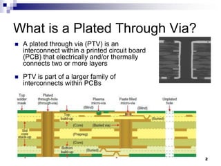
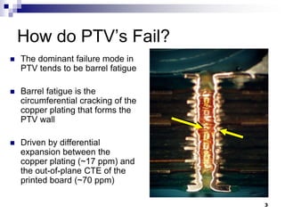


The document discusses the design and reliability of plated through-vias (PTVs) in printed circuit boards (PCBs), highlighting the primary failure mode of barrel fatigue related to thermal expansion differences. It outlines the critical parameters affecting PTV reliability including height, diameter, and material properties, as well as manufacturing challenges such as plating thickness and drilling processes. The document emphasizes the importance of thorough testing and qualification procedures to ensure PTV performance under thermal stress conditions.