Downloaded 493 times


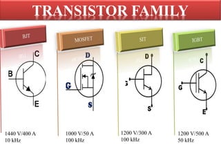
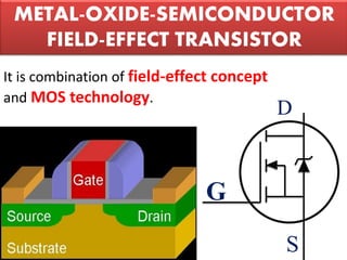
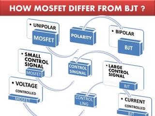
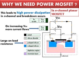
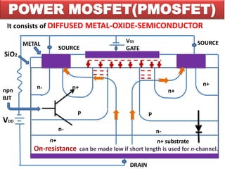
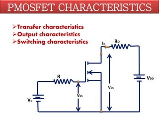
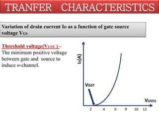
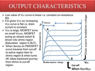
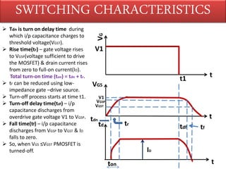


This document discusses power MOSFETs, including their characteristics and advantages over bipolar junction transistors. Some key points: 1) Power MOSFETs can operate at high voltages up to 1400V and high currents up to 500A, with switching frequencies ranging from 10-100kHz depending on the device. 2) Power MOSFETs use a metal-oxide-semiconductor field-effect transistor design that allows the gate voltage to fully control the channel conductance. 3) Their on-resistance can be made very low, allowing them to operate efficiently at high power levels before breakdown occurs. This makes them well-suited for applications requiring high power switching.


