What is Nano?
• Nano- a prefix that means very, very, small !
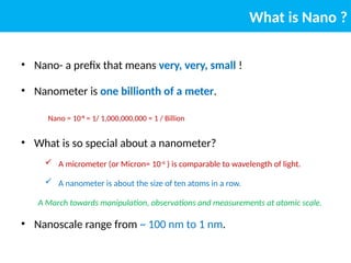
• Nanometer is one billionth of a meter.
Nano = 10-9
= 1/ 1,000,000,000 = 1 / Billion
• What is so special about a nanometer?
A micrometer (or Micron= 10-6
) is comparable to wavelength of light.
A nanometer is about the size of ten atoms in a row.
A March towards manipulation, observations and measurements at atomic scale.
• Nanoscale range from ~ 100 nm to 1 nm.
4.
What is Nano-Science?
• A part of science that studies small stuff.
• Nanoscience is not physics or chemistry or engineering
or biology. Rather it is multidisciplinary in nature.
• It can be envisioned as realm of Materials Science
when constituent units lie in nano-scale and exhibit
abrupt changes in properties which may be tunable
too.
5.
• A biologicalsystem can be exceedingly small. Most cells are
tiny but very active. They
manufacture various substances.
walk around, wriggle and do all kinds of marvelous things—all on a very small scale.
store information.
• Consider the possibility that, we too, can make a thing, that
is very small and does what we want.
Introduction to Nano-Systems
6.
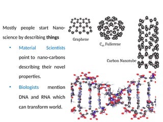
Mostly people startNano-
science by describing things
• Material Scientists
point to nano-carbons
describing their novel
properties.
• Biologists mention
DNA and RNA which
can transform world.
Graphene
C60 Fullerene
Carbon Nanotube
7.
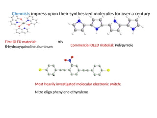
Chemists impress upontheir synthesized molecules for over a century
First OLED material: tris
8-hydroxyquinoline aluminum
Most heavily investigated molecular electronic switch:
Nitro oligo phenylene ethynylene
Commercial OLED material: Polypyrrole
8.
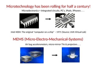
Microtechnology has beenrolling for half a century!
Microelectronics = Integrated circuits, PC's, iPods, iPhones . . .
Intel 4004: The original "computer on a chip" - 1971 (Source: UVA Virtual Lab)
MEMS (Micro-Electro-Mechanical-Systems)
Air bag accelerometers, micro-mirror TVs & projectors . . .
9.
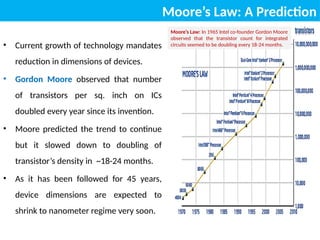
• Current growthof technology mandates
reduction in dimensions of devices.
• Gordon Moore observed that number
of transistors per sq. inch on ICs
doubled every year since its invention.
• Moore predicted the trend to continue
but it slowed down to doubling of
transistor’s density in ~18-24 months.
• As it has been followed for 45 years,
device dimensions are expected to
shrink to nanometer regime very soon.
Moore’s Law: In 1965 Intel co-founder Gordon Moore
observed that the transistor count for integrated
circuits seemed to be doubling every 18-24 months.
Moore’s Law: A Prediction
10.
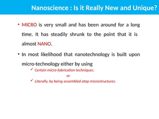
Nanoscience : Isit Really New and Unique?
• MICRO is very small and has been around for a long
time. It has steadily shrunk to the point that it is
almost NANO.
• In most likelihood that nanotechnology is built upon
micro-technology either by using
Certain micro-fabrication techniques.
or
Literally, by being assembled atop microstructures.
11.
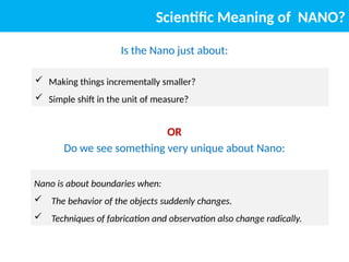
Scientific Meaning ofNANO?
Is the Nano just about:
OR
Do we see something very unique about Nano:
Nano is about boundaries when:
The behavior of the objects suddenly changes.
Techniques of fabrication and observation also change radically.
Making things incrementally smaller?
Simple shift in the unit of measure?
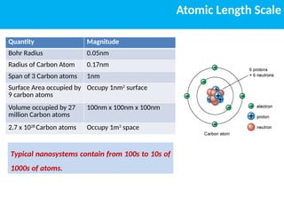
Typical nanosystems containfrom 100s to 10s of
1000s of atoms.
Atomic Length Scale
Quantity Magnitude
Bohr Radius 0.05nm
Radius of Carbon Atom 0.17nm
Span of 3 Carbon atoms 1nm
Surface Area occupied by
9 carbon atoms
Occupy 1nm2
surface
Volume occupied by 27
million Carbon atoms
100nm x 100nm x 100nm
2.7 x 1028
Carbon atoms Occupy 1m3
space
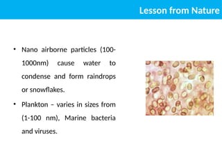
• Nano airborneparticles (100-
1000nm) cause water to
condense and form raindrops
or snowflakes.
• Plankton – varies in sizes from
(1-100 nm), Marine bacteria
and viruses.
Lesson from Nature
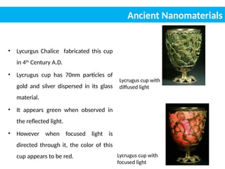
16.
• Lycurgus Chalicefabricated this cup
in 4th
Century A.D.
• Lycrugus cup has 70nm particles of
gold and silver dispersed in its glass
material.
• It appears green when observed in
the reflected light.
• However when focused light is
directed through it, the color of this
cup appears to be red.
Lycrugus cup with
diffused light
Lycrugus cup with
focused light
Ancient Nanomaterials
17.
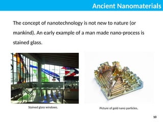
Ancient Nanomaterials
Stained glasswindows. Picture of gold nano particles.
10
The concept of nanotechnology is not new to nature (or
mankind). An early example of a man made nano-process is
stained glass.
18.
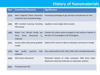
History of Nanomaterials
YearInvention/Discovery Significance
1974 Nario Taniguchi (Tokyo University)
coined the term Nanotechnology.
Processing technology to get precision and tolerance of 1nm.
1981 IBM invented Scanning Tunneling
Microscope.
Capable to move single atoms around.
1985 Robert Curl, Richard Smally and
Harry Kroto discovered C60
molecule.
Contains 60 carbon atoms arranged on the surface of sphere in
the form of 12 pentagons and 20 hexagons.
1991 Sumino Lijima discovered graphitic
needle
Made of CNT and are 4-30nm in diameter and micron in length.
1993 High quality quantum dots
prepared
Very small particles (CdS, CdSe, CdTe) with controlled diameters.
2000 DNA motors discovered Motorized twizzers to make computers 1000 times faster.
Attached to electrical molecules to make basic switches.
2001 Prototype fuel cells
19.
Feynman’s Insight
• There'sPlenty of Room at the Bottom was a lecture given
by physicist Richard Feynman at an American Physical
Society meeting at Caltech on December 29, 1959.
• Feynman considered the possibility of direct manipulation
of individual atoms as a more powerful form of synthetic
chemistry than contemporary processes in use.
• The talk went unnoticed and did not inspire the conceptual
beginnings of the field.
• In 1990s it was rediscovered and publicised as a seminal
event in the field, probably to boost the history of
nanotechnology with Feynman's reputation.
20.
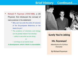
Brief History Continued……
SurelyYou’re Joking
Mr. Feynman!
Adventures of a Curious
Character
By Richard Feynman
Richard P. Feynman (1918-1988), a US
Physicist, first introduced the concept of
nano-science in his statement:
Why can’t we write the entire 24 volumes
of the Encyclopedia Britannica on the
head of a pin?
The problems of chemistry and biology
can be greatly helped if we develop
o ability to see what we are doing
&
o do things on an atomic level
A development, which I think is unavoidable.
21.
Brief History Continued….
Birthof Nanotechnology
Professor Nario Taniguchi of Tokyo
Science University used the word
nanotechnology to describe the
science and technology of processing
or building parts with nano-metric
tolerance.
11
22.
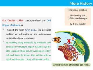
More History
Engines ofCreation
The Coming Era
of Nanotechnology
By K. Eric Drexler
Eric Drexler (1986) conceptualized the Cell
Repair Machines as:
Coined the term Grey Goo… the potential
problem of self-replicating and autonomous
artificial intelligence machines.
By working along molecule by molecule and
structure by structure, repair machines will be
able to repair whole cell. By working on cell by
cell and tissue by tissue, they will be able to
repair whole organ……they will restore health.
X
Stylized example of targeted cell repair.
23.
Brief History, Continued
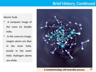
AtomicScale
• A computer image of
the nano ice double
helix.
• In the nano-ice image,
oxygen atoms are blue
in the inner helix,
purple in the outer
helix. Hydrogen atoms
are white.
A nanotechnology self-assembly process. 14
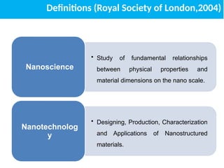
Definitions (Royal Societyof London,2004)
• Study of fundamental relationships
between physical properties and
material dimensions on the nano scale.
Nanoscience
• Designing, Production, Characterization
and Applications of Nanostructured
materials.
Nanotechnolog
y
26.
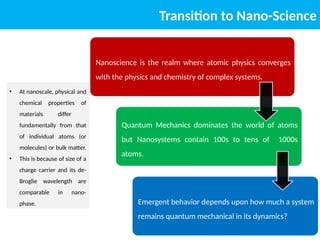
Transition to Nano-Science
Nanoscienceis the realm where atomic physics converges
with the physics and chemistry of complex systems.
Quantum Mechanics dominates the world of atoms
but Nanosystems contain 100s to tens of 1000s
atoms.
Emergent behavior depends upon how much a system
remains quantum mechanical in its dynamics?
• At nanoscale, physical and
chemical properties of
materials differ
fundamentally from that
of individual atoms (or
molecules) or bulk matter.
• This is because of size of a
charge carrier and its de-
Broglie wavelength are
comparable in nano-
phase.
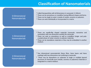
• Called Nanoparticleswith all dimensions in nanoscale (1-100nm).
• These can be amorphous or crystalline having different shapes and forms.
• These can be single (or poly-) crystals of metals, ceramics or polymers.
• These can exist individually or incorporated in a matrix.
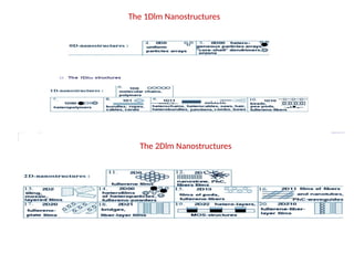
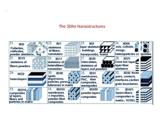
0-Dimensional
Nanomaterials
• These are needle-like shaped materials (nanorods, nanowires and
nanotubes) with one dimension outside the nanoscale.
• These can exist as amorphous as well as crystalline (single- and poly-
crystals) phase of metal, ceramic or polymer materials.
• These can be standalone materials or they may be embedded in another
medium.
1-Dimensional
Nanomaterials
• Two dimensional nanomaterials (Nano films, Nano layers and Nano
coatings) with two dimensions not confining to nanoscale.
• These may be depositions on substrate of single or multiple layered
structures of chemically pure (metals, ceramics or polymers) materials or
integrated in a matrix medium.
2-Dimensional
Nanomaterials
Classification of Nanomaterials
29.
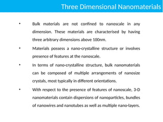
Three Dimensional Nanomaterials
•Bulk materials are not confined to nanoscale in any
dimension. These materials are characterised by having
three arbitrary dimensions above 100nm.
• Materials possess a nano-crystalline structure or involves
presence of features at the nanoscale.
• In terms of nano-crystalline structure, bulk nanomaterials
can be composed of multiple arrangements of nanosize
crystals, most typically in different orientations.
• With respect to the presence of features of nanoscale, 3-D
nanomaterials contain dispersions of nanoparticles, bundles
of nanowires and nanotubes as well as multiple nano-layers.
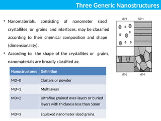
Three Generic Nanostructures
•Nanomaterials, consisting of nanometer sized
crystallites or grains and interfaces, may be classified
according to their chemical composition and shape
(dimensionality).
• According to the shape of the crystallites or grains,
nanomaterials are broadly classified as:
Nanostructures Definition
MD=0 Clusters or powder
MD=1 Multilayers
MD=2 Ultrafine grained over-layers or buried
layers with thickness less than 50nm
MD=3 Equiaxed nanometer sized grains.
32.
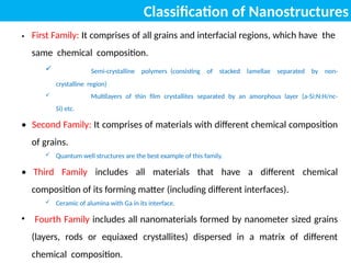
Classification of Nanostructures
•First Family: It comprises of all grains and interfacial regions, which have the
same chemical composition.
Semi-crystalline polymers (consisting of stacked lamellae separated by non-
crystalline region)
Multilayers of thin film crystallites separated by an amorphous layer (a-Si:N:H/nc-
Si) etc.
• Second Family: It comprises of materials with different chemical composition
of grains.
Quantum well structures are the best example of this family.
• Third Family includes all materials that have a different chemical
composition of its forming matter (including different interfaces).
Ceramic of alumina with Ga in its interface.
• Fourth Family includes all nanomaterials formed by nanometer sized grains
(layers, rods or equiaxed crystallites) dispersed in a matrix of different
chemical composition.
33.
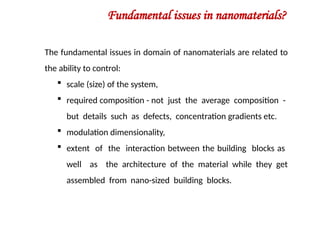
Fundamental issues innanomaterials?
The fundamental issues in domain of nanomaterials are related to
the ability to control:
scale (size) of the system,
required composition - not just the average composition -
but details such as defects, concentration gradients etc.
modulation dimensionality,
extent of the interaction between the building blocks as
well as the architecture of the material while they get
assembled from nano-sized building blocks.
34.
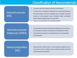
Classification of Nanomaterials
•A structure with d<dc(=100nm) at least for one dimension.
• The value of dc is dictated by characteristic of one physical phenomena
(free path length of electron, de-Broglie wave and length of external
acoustic or electromagnetic wave, correlation length, penetration
length, diffusion length) giving rise to size effects.
• These are characterized by form and dimensionality.
Nanostructures
(NS)
• Low dimensional materials composing of building units of a submicron
or nanoscale size at least in one direction and exhibiting size effects.
• Nanostructured materials are characterized by form, dimensionality
and composition.
Nanostructured
Materials (NSM)
• Nanocomposite materials (two or more component materials) cover a
vast range of ceramic, metallic and cero-metallic materials in the form
of bulk materials and thin films.
Nanocomposites
(NC)
35.
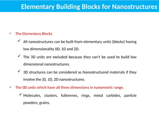
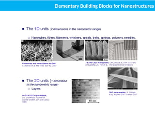
Elementary Building Blocksfor Nanostructures
• The Elementary Blocks
All nanostructures can be built from elementary units (blocks) having
low dimensionality 0D, 1D and 2D.
The 3D units are excluded because they can’t be used to build low
dimensional nanostructures.
3D structures can be considered as Nanostructured materials if they
involve the )D, 1D, 2D nanostructures.
• The 0D units which have all three dimensions in nanometric range.
Molecules, clusters, fullerenes, rings, metal carbides, particle
powders, grains.
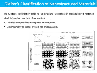
Gleiter’s Classification ofNanostructured Materials
The Gleiter’s classification leads to 12 structural categories of nanostructured materials
which is based on two type of parameters:
Chemical composition: monophase or multiphase.
Dimensionality or shape: layered, rod and equiaxed.
38.
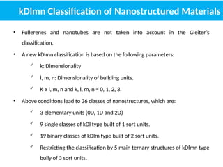
kDlmn Classification ofNanostructured Materials
• Fullerenes and nanotubes are not taken into account in the Gleiter’s
classification.
• A new kDlmn classification is based on the following parameters:
k: Dimensionality
l, m, n: Dimensionality of building units.
K ≥ l, m, n and k, l, m, n = 0, 1, 2, 3.
• Above conditions lead to 36 classes of nanostructures, which are:
3 elementary units (0D, 1D and 2D)
9 single classes of kDl type built of 1 sort units.
19 binary classes of kDlm type built of 2 sort units.
Restricting the classification by 5 main ternary structures of kDlmn type
buily of 3 sort units.
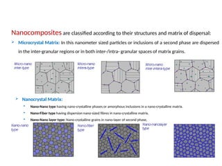
Nanocomposites are classifiedaccording to their structures and matrix of dispersal:
Microcrystal Matrix: In this nanometer sized particles or inclusions of a second phase are dispersed
in the inter-granular regions or in both inter-/intra- granular spaces of matrix grains.
Nanocrystal Matrix:
Nano-Nano type having nano-crystalline phases or amorphous inclusions in a nano-crystalline matrix.
Nano-Fiber type having dispersion nano-sized fibres in nano-crystalline matrix.
Nano-Nano layer type: Nano-crystalline grains in nano-layer of second phase,
42.
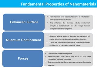
Fundamental Properties ofNanomaterials
• Nanomaterials have larger surface area to volume ratio
relative to matter in bulk form.
• This enhances the chemical activity, mechanical
strength of nanomaterials and also brings marked
changes in electrical properties.
Enhanced Surface
Forces
• Quantum effects begin to dominate the behaviour of
matter at the Nanoscale due to spatial confinement.
• This is the root cause of altogether different properties
exhibited by as compared to its bulk phase.
Quantum Confinement
• Gravitational forces are negligible.
• Electromagnetic force which may short or long range
correlations guide the behaviour.
• Quantum mechanical forces such as exchange forces also
play role.
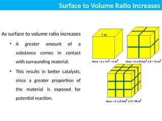
Surface to VolumeRatio Increases
As surface to volume ratio increases
• A greater amount of a
substance comes in contact
with surrounding material.
• This results in better catalysts,
since a greater proportion of
the material is exposed for
potential reaction.
45.
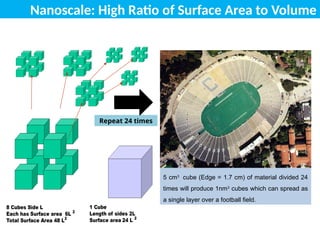
5 cm3
cube (Edge= 1.7 cm) of material divided 24
times will produce 1nm3
cubes which can spread as
a single layer over a football field.
Repeat 24 times
Nanoscale: High Ratio of Surface Area to Volume
46.
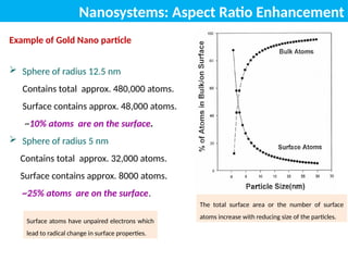
Nanosystems: Aspect RatioEnhancement
Example of Gold Nano particle
Sphere of radius 12.5 nm
Contains total approx. 480,000 atoms.
Surface contains approx. 48,000 atoms.
~10% atoms are on the surface.
Sphere of radius 5 nm
Contains total approx. 32,000 atoms.
Surface contains approx. 8000 atoms.
~25% atoms are on the surface.
Surface atoms have unpaired electrons which
lead to radical change in surface properties.
The total surface area or the number of surface
atoms increase with reducing size of the particles.
47.
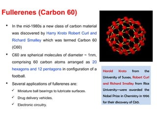
In themid-1980s a new class of carbon material
was discovered by Harry Kroto Robert Curl and
Richard Smalley which was termed Carbon 60
(C60)
C60 are spherical molecules of diameter ~ 1nm,
comprising 60 carbon atoms arranged as 20
hexagons and 12 pentagons in configuration of a
football.
Several applications of fullerenes are:
Miniature ball bearings to lubricate surfaces.
Drug delivery vehicles.
Electronic circuitry.
Fullerenes (Carbon 60)
Harold Kroto from the
University of Sussex, Robert Curl
and Richard Smalley from Rice
University—were awarded the
Nobel Prize in Chemistry in 1996
for their discovery of C60.
48.
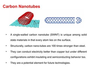
Carbon Nanotubes
• Asingle-walled carbon nanotube (SWNT) is unique among solid
state materials in that every atom lies on the surface.
• Structurally, carbon nano-tubes are 100 times stronger than steel.
• They can conduct electricity better than copper but under different
configurations exhibit insulating and semiconducting behavior too.
• They are a potential element for future technologies.
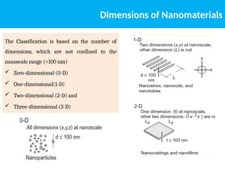
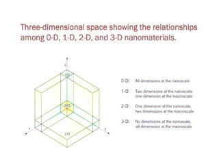
Dimensions of Nanomaterials
TheClassification is based on the number of
dimensions, which are not confined to the
nanoscale range (<100 nm)
Zero-dimensional (0-D)
One-dimensional(1-D)
Two-dimensional (2-D) and
Three-dimensional (3-D)
51.
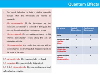
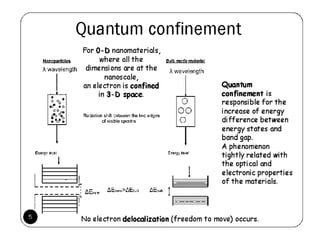
Quantum Effects
• Theoverall behaviour of bulk crystalline materials
changes when the dimensions are reduced to
nanoscale.
• 0-D nanomaterials: All the dimensions are the
nanoscale and electron is confined in 3-D space. No
electron delocalization (freedom to move) occurs.
• 1-D nanomaterials: Electron confinement occurs in 2-D
whereas delocalization occurs along the axis of
nanowire/rod/tube.
• 2-D nanomaterials: the conduction electrons will be
confined across the thickness but delocalized exists in
the plane of the sheet.
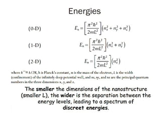
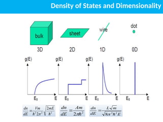
0-D nanomaterials: Electrons are fully confined.
3-D materials: Electrons are fully delocalized.
1-D & 2-D nanomaterials: Electron confinement and
delocalization coexists.
Structure Spatial
Dimensions
Confinement
Dimensions
Bulk 3 0
Quantum Well
Surface
Films
2 1
Quantum wire
Nanotubes
Nanowires
1 2
Quantum dots
Cluster
Nanoparticles
0 3
53.
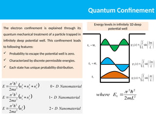
Quantum Confinement
The electronconfinement is explained through its
quantum mechanical treatment of a particle trapped in
infinitely deep potential well. This confinement leads
to following features:
Probability to escape the potential well is zero.
Characterized by discrete permissible energies.
Each state has unique probability distribution.
L
x
L
x
2
sin
2
)
(
2
L
x
L
x
3
sin
2
)
(
3
E1
E3 = 9E1
L
x
L
x
sin
2
)
(
1
E2 = 4E1
Energy levels in infinitely 1D deep
potential well
2
2
2
1
2mL
E
where
al
Nanomateri
D
n
ma
E
al
Nanomateri
D
n
n
ma
E
al
Nanomateri
D
n
n
n
ma
E
x
y
x
z
y
x
2
2
1
2
0
2
2
2
2
2
2
2
2
2
2
2
2
2
2
2
2
55.
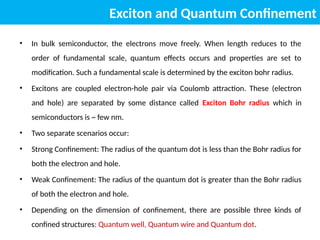
Exciton and QuantumConfinement
• In bulk semiconductor, the electrons move freely. When length reduces to the
order of fundamental scale, quantum effects occurs and properties are set to
modification. Such a fundamental scale is determined by the exciton bohr radius.
• Excitons are coupled electron-hole pair via Coulomb attraction. These (electron
and hole) are separated by some distance called Exciton Bohr radius which in
semiconductors is ~ few nm.
• Two separate scenarios occur:
• Strong Confinement: The radius of the quantum dot is less than the Bohr radius for
both the electron and hole.
• Weak Confinement: The radius of the quantum dot is greater than the Bohr radius
of both the electron and hole.
• Depending on the dimension of confinement, there are possible three kinds of
confined structures: Quantum well, Quantum wire and Quantum dot.
56.
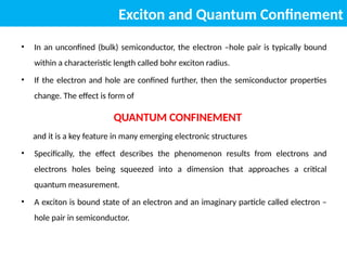
Exciton and QuantumConfinement
• In an unconfined (bulk) semiconductor, the electron –hole pair is typically bound
within a characteristic length called bohr exciton radius.
• If the electron and hole are confined further, then the semiconductor properties
change. The effect is form of
QUANTUM CONFINEMENT
and it is a key feature in many emerging electronic structures
• Specifically, the effect describes the phenomenon results from electrons and
electrons holes being squeezed into a dimension that approaches a critical
quantum measurement.
• A exciton is bound state of an electron and an imaginary particle called electron –
hole pair in semiconductor.
58.
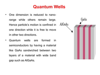
Quantum Wells
• Onedimension is reduced to nano-
range while others remain large.
Hence particle’s motion is confined in
one direction while it is free to move
in other two directions.
• Quantum wells are formed in
semiconductors by having a material
like GaAs sandwiched between two
layers of a material with wide band
gap such as AlGaAs.
59.
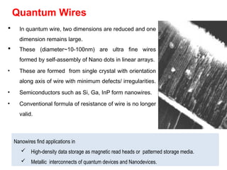
Quantum Wires
Inquantum wire, two dimensions are reduced and one
dimension remains large.
These (diameter~10-100nm) are ultra fine wires
formed by self-assembly of Nano dots in linear arrays.
• These are formed from single crystal with orientation
along axis of wire with minimum defects/ irregularities.
• Semiconductors such as Si, Ga, InP form nanowires.
• Conventional formula of resistance of wire is no longer
valid.
Nanowires find applications in
High-density data storage as magnetic read heads or patterned storage media.
Metallic interconnects of quantum devices and Nanodevices.
60.
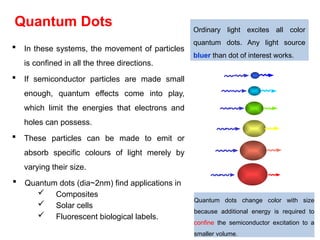
In thesesystems, the movement of particles
is confined in all the three directions.
If semiconductor particles are made small
enough, quantum effects come into play,
which limit the energies that electrons and
holes can possess.
These particles can be made to emit or
absorb specific colours of light merely by
varying their size.
Quantum dots (dia~2nm) find applications in
Composites
Solar cells
Fluorescent biological labels.
Quantum Dots Ordinary light excites all color
quantum dots. Any light source
bluer than dot of interest works.
Quantum dots change color with size
because additional energy is required to
confine the semiconductor excitation to a
smaller volume.
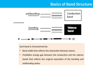
Basics of BandStructure
Each band is characterised by:
• Band width that reflects the interaction between atoms,
• Forbidden energy gap between the conduction and the valence
bands that reflects the original separation of the bonding and
antibonding states.
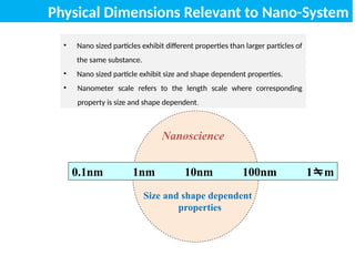
0.1nm 1nm 10nm100nm 1m
Nanoscience
Size and shape dependent
properties
Physical Dimensions Relevant to Nano-System
• Nano sized particles exhibit different properties than larger particles of
the same substance.
• Nano sized particle exhibit size and shape dependent properties.
• Nanometer scale refers to the length scale where corresponding
property is size and shape dependent.
66.
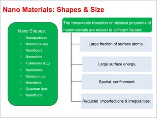
Nano Materials: Shapes& Size
Nano Shapes:
o Nanoparticles
o Nanocapsules
o Nanofibers
o Nanowires
o Fullerenes (C60)
o Nanotubes
o Nanosprings
o Nanobelts
o Quantum dots
o Nanofluids
The remarkable transition of physical properties of
nanomaterials are related to different factors:
Large fraction of surface atoms.
Large surface energy.
Spatial confinement.
Reduced imperfections & irregularities.
67.
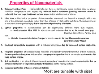
Properties of Nanomaterials
1.Reduced Melting Point -- Nanomaterials may have a significantly lower melting point or phase
transition temperature and appreciably reduced lattice constants (spacing between atoms is
reduced), due to a huge fraction of surface atoms in the total amount of atoms.
2. Ultra Hard -- Mechanical properties of nanomaterials may reach the theoretical strength, which are
one or two orders of magnitude higher than that of single crystals in the bulk form. The enhancement
in mechanical strength is simply due to the reduced probability of defects.
3. Optical properties of nanomaterials can be significantly different from bulk crystals.
--- Semiconductor Blue Shift in adsorption and emission due to an increased band gap.
Quantum Size Effects, Particle in a
box.
--- Metallic Nanoparticles Color Changes in spectra due to Surface Plasmons Resonances
Lorentz Oscillator Model.
4. Electrical conductivity decreases with a reduced dimension due to increased surface scattering.
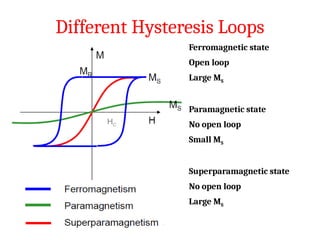
5. Magnetic properties of nanostructured materials are distinctly different from that of bulk materials.
Ferromagnetism disappears and transfers to superparamagnetism in the nanometer scale due to the
huge surface energy.
6. Self-purification is an intrinsic thermodynamic property of nanostructures and nanomaterials due to
enhanced diffusion of impurities/defects/dislocations to the nearby surface.
7. Increased perfection enhances chemical stability.
Most are tunable with size!
68.
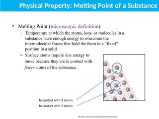
Physical Property: MeltingPoint of a Substance
• Melting Point (microscopic definition)
– Temperature at which the atoms, ions, or molecules in a
substance have enough energy to overcome the
intermolecular forces that hold the them in a “fixed”
position in a solid
– Surface atoms require less energy to
move because they are in contact with
fewer atoms of the substance.
In contact with 3 atoms
In contact with 7 atoms
http://serc.carleton.edu/usingdata/nasaimages/index4.html
69.
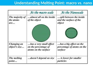
At the macroscale At the Nanoscale
The majority of
the atoms
are…
…almost all on the inside
of the object
…split between the inside
and the surface of the
object
Changing an
object’s size…
…has a very small effect
on the percentage of
atoms on the surface
…has a big effect on the
percentage of atoms on the
surface
The melting
point…
…doesn’t depend on size … is lower for smaller
particles
Understanding Melting Point: macro vs. nano
70.
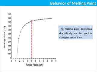
The melting pointdecreases
dramatically as the particle
size gets below 5 nm.
Behavior of Melting Point
71.
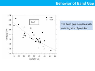
Behavior of BandGap
The band gap increases with
reducing size of particles.
72.
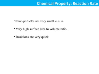
Chemical Property: ReactionRate
• Nano particles are very small in size.
• Very high surface area to volume ratio.
• Reactions are very quick.
73.
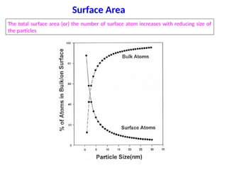
Surface Area
The totalsurface area (or) the number of surface atom increases with reducing size of
the particles
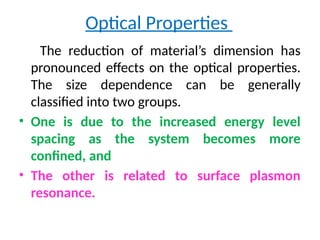
Optical Properties
The reductionof material’s dimension has
pronounced effects on the optical properties.
The size dependence can be generally
classified into two groups.
• One is due to the increased energy level
spacing as the system becomes more
confined, and
• The other is related to surface plasmon
resonance.
76.
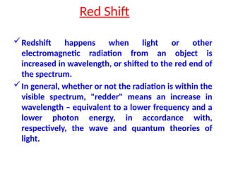
Red Shift
Redshift happenswhen light or other
electromagnetic radiation from an object is
increased in wavelength, or shifted to the red end of
the spectrum.
In general, whether or not the radiation is within the
visible spectrum, "redder" means an increase in
wavelength – equivalent to a lower frequency and a
lower photon energy, in accordance with,
respectively, the wave and quantum theories of
light.
77.
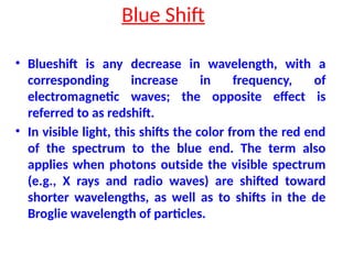
Blue Shift
• Blueshiftis any decrease in wavelength, with a
corresponding increase in frequency, of
electromagnetic waves; the opposite effect is
referred to as redshift.
• In visible light, this shifts the color from the red end
of the spectrum to the blue end. The term also
applies when photons outside the visible spectrum
(e.g., X rays and radio waves) are shifted toward
shorter wavelengths, as well as to shifts in the de
Broglie wavelength of particles.
78.
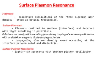
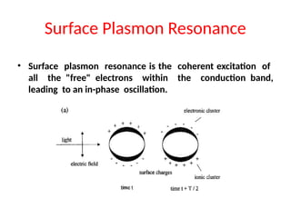
Surface Plasmon Resonance
Plasmons:
-collective oscillations of the “free electron gas”
density, often at optical frequencies.
Surface Plasmons:
- Plasmons confined to surface (interface) and interact
with light resulting in polaritons.
Polaritons are quasiparticles resulting from strong coupling of electromagnetic waves
with an electric or magnetic dipole-carrying excitation.
- propagating electron density waves occurring at the
interface between metal and dielectric.
Surface Plasmon Resonance:
- light () in resonance with surface plasmon oscillation
79.
Surface Plasmon Resonance
•Surface plasmon resonance is the coherent excitation of
all the "free" electrons within the conduction band,
leading to an in-phase oscillation.
80.
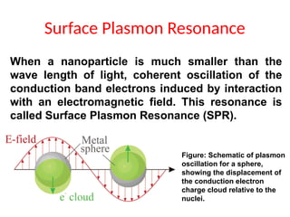
Surface Plasmon Resonance
Figure:Schematic of plasmon
oscillation for a sphere,
showing the displacement of
the conduction electron
charge cloud relative to the
nuclei.
When a nanoparticle is much smaller than the
wave length of light, coherent oscillation of the
conduction band electrons induced by interaction
with an electromagnetic field. This resonance is
called Surface Plasmon Resonance (SPR).
81.
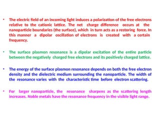
• The electricfield of an incoming light induces a polarization of the free electrons
relative to the cationic lattice. The net charge difference occurs at the
nanoparticle boundaries (the surface), which in turn acts as a restoring force. In
this manner a dipolar oscillation of electrons is created with a certain
frequency.
• The surface plasmon resonance is a dipolar excitation of the entire particle
between the negatively charged free electrons and its positively charged lattice.
• The energy of the surface plasmon resonance depends on both the free electron
density and the dielectric medium surrounding the nanoparticle. The width of
the resonance varies with the characteristic time before electron scattering.
• For larger nanoparticle, the resonance sharpens as the scattering length
increases. Noble metals have the resonance frequency in the visible light range.
82.
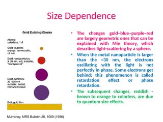
Size Dependence
• Thechanges gold–blue–purple–red
are largely geometric ones that can be
explained with Mie theory, which
describes light-scattering by a sphere.
• When the metal nanoparticle is larger
than the ~30 nm, the electrons
oscillating with the light is not
perfectly in phase. Some electrons get
behind; this phenomenon is called
retardation effect or phase
retardation.
• The subsequent changes, reddish -
brown to orange to colorless, are due
to quantum size effects.
Mulvaney, MRS Bulletin 26, 1009 (1996)
Electrical Conductivity
These mechanismscan be generally grouped into THREE categories:
A. Change of electronic structure
B. Change of microstructure
C. Quantum Effects
In addition, increased perfection, such as reduced impurity, structural defects and
dislocations, would affect the electrical conductivity of nanostructures.
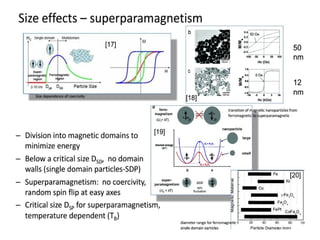
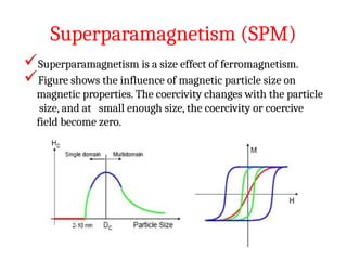
Superparamagnetism (SPM)
Superparamagnetism isa size effect of ferromagnetism.
Figure shows the influence of magnetic particle size on
magnetic properties. The coercivity changes with the particle
size, and at small enough size, the coercivity or coercive
field become zero.
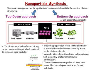
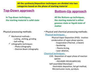
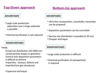
CHEMICAL METHODS OFSYNTHESIS
• Hydrothermal Method
• Sol-Gel Method
• Micro-Emulsion Technique
• Spray Pyrolysis
• Flame Spray Pyrolysis
• Chemical Vapour Deposition
• Chemical Bath Technique
• Colloidal Methods
• Chemical Reduction of Salts
• Electrochemical Synthesis
98.
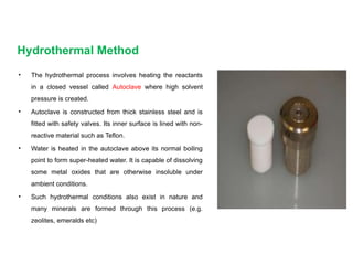
Hydrothermal Method
• Thehydrothermal process involves heating the reactants
in a closed vessel called Autoclave where high solvent
pressure is created.
• Autoclave is constructed from thick stainless steel and is
fitted with safety valves. Its inner surface is lined with non-
reactive material such as Teflon.
• Water is heated in the autoclave above its normal boiling
point to form super-heated water. It is capable of dissolving
some metal oxides that are otherwise insoluble under
ambient conditions.
• Such hydrothermal conditions also exist in nature and
many minerals are formed through this process (e.g.
zeolites, emeralds etc)
99.
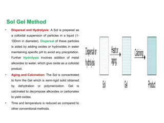
Sol Gel Method
•Dispersal and Hydrolysis: A Sol is prepared as
a colloidal suspension of particles in a liquid (1-
100nm in diameter). Dispersal of these particles
is aided by adding oxides or hydroxides in water
maintaining specific pH to avoid any precipitation.
Further Hydrolysis involves addition of metal
alkoxides to water, which give oxide as a colloidal
product.
• Aging and Calcination: The Sol is concentrated
to form the Gel which is semi-rigid solid obtained
by dehydration or polymerization. Gel is
calcinated to decompose alkoxides or carbonates
to yield oxides.
• Time and temperature is reduced as compared to
other conventional methods.
100.
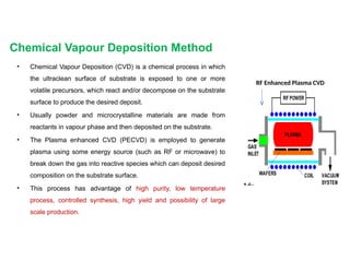
Chemical Vapour DepositionMethod
• Chemical Vapour Deposition (CVD) is a chemical process in which
the ultraclean surface of substrate is exposed to one or more
volatile precursors, which react and/or decompose on the substrate
surface to produce the desired deposit.
• Usually powder and microcrystalline materials are made from
reactants in vapour phase and then deposited on the substrate.
• The Plasma enhanced CVD (PECVD) is employed to generate
plasma using some energy source (such as RF or microwave) to
break down the gas into reactive species which can deposit desired
composition on the substrate surface.
• This process has advantage of high purity, low temperature
process, controlled synthesis, high yield and possibility of large
scale production.
RF Enhanced Plasma CVD
101.
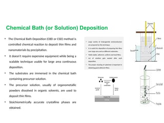
Chemical Bath (orSolution) Deposition
• The Chemical Bath Deposition (CBD or CSD) method is
controlled chemical reaction to deposit thin films and
nanomaterials by precipitation.
• It doesn’t require expensive equipment while being a
scalable technique usable for large area continuous
deposition.
• The substrates are immersed in the chemical bath
containing precursor solution.
• The precursor solution, usually of organometallic
powders dissolved in organic solvents, are used to
deposit thin films.
• Stoichiometrically accurate crystalline phases are
obtained.
• Large variety of chalcogenide semiconductors
are prepared by this technique.
• It is useful for deposition of preparing thin films
over large area and on different substrates.
• Yields stable, adherent, uniform and hard films.
• Lot of solution gets wasted after each
deposition.
• The proper cleaning of substrate is important in
obtaining good adherent films.
102.
Colloidal Methods
• Itis the most useful, easiest, and cheapest way to create nanoparticles.
• It may utilize both organic and inorganic reactants.
• A metal salt is reduced leaving nanoparticles evenly dispersed in a liquid.
• Aggregation is prevented by the introduction of a stabilizing reagent that
coats the particle surfaces.
• Particle sizes range from 1-200nm and are controlled by the initial
concentrations of the reactants and the action of the stabilizing reagent.
103.
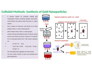
Colloidal Methods: Synthesisof Gold Nanoparticles
– A common method for preparing colloidal gold
nanoparticles involves combining hydrogen tetra-chloro-
aurate (HAuCl4) and sodium citrate (Na3C6H5O7) in a dilute
solution.
– Heat a solution of chloroauric acid (HAuCl4) up to reflux
(boiling). HAuCl4 is a water soluble gold salt.
• Add tri-sodium citrate, which is a reducing agent.
• Continue stirring and heating for about 10 minutes. During
this time, the citrate ions (C6H5O7
3-
) reduce Au3+
to yield 30-
40 nm metal gold particles (Au0
). Half reaction equations
are:
Au3+(
aq) + 3e-
Au(s)
C6H5O7
3-
(aq) +H2O(l) C5H4O4
2-
(aq) + CO2(g) +
H3O(aq) + 2e-
– The neutral gold atoms aggregate into seed crystals.
– The seed crystals continue to grow and eventually form
gold nanoparticles.
HAuCl4
Gold
NP
HAuCl4
Sodium
Citrate
Heat
Reduction of gold ions: Au(III) + 3e-
→ Au(0)
Nucleation of Au(0) seed crystals:
Seed Crystal
10’s to 100’s of Atoms
Nanorod
s
Spherical
Nanoparticles
Isotropic
Growth
Anisotropic Growth
Surface capped
with citrate anions
Adding surfactant to growth
solution caps certain crystal
faces and promotes growth only
in selected directions.
Growth of nanoparticles:
Seed
104.
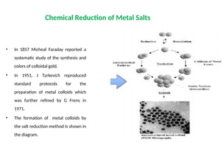
Chemical Reduction ofMetal Salts
• In 1857 Micheal Faraday reported a
systematic study of the synthesis and
colors of colloidal gold.
• In 1951, J Turkevich reproduced
standard protocols for the
preparation of metal colloids which
was further refined by G Frens in
1971.
• The formation of metal colloids by
the salt reduction method is shown in
the diagram.
105.
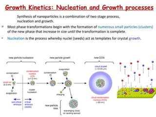
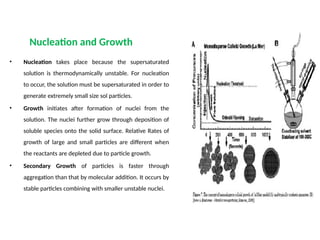
Nucleation and Growth
•Nucleation takes place because the supersaturated
solution is thermodynamically unstable. For nucleation
to occur, the solution must be supersaturated in order to
generate extremely small size sol particles.
• Growth initiates after formation of nuclei from the
solution. The nuclei further grow through deposition of
soluble species onto the solid surface. Relative Rates of
growth of large and small particles are different when
the reactants are depleted due to particle growth.
• Secondary Growth of particles is faster through
aggregation than that by molecular addition. It occurs by
stable particles combining with smaller unstable nuclei.
106.
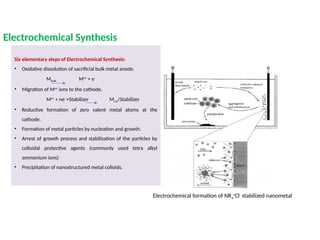
Electrochemical Synthesis
Six elementarysteps of Electrochemical Synthesis:
• Oxidative dissolution of sacrificial bulk metal anode.
Mbulk Mn+
+ e-
• Migration of Mn+
ions to the cathode.
Mn+
+ ne-
+Stabilizer Mcol/Stabilizer
• Reductive formation of zero valent metal atoms at the
cathode.
• Formation of metal particles by nucleation and growth.
• Arrest of growth process and stabilization of the particles by
colloidal protective agents (commonly used tetra alkyl
ammonium ions)
• Precipitation of nanostructured metal colloids.
Electrochemical formation of NR4
+
Cl-
stabilized nanometal
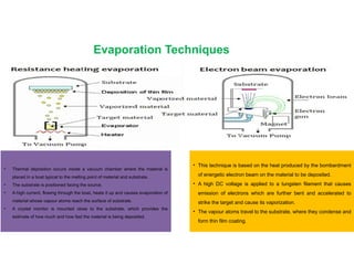
Evaporation Techniques
• Thermaldeposition occurs inside a vacuum chamber where the material is
placed in a boat typical to the melting point of material and substrate.
• The substrate is positioned facing the source.
• A high current, flowing through the boat, heats it up and causes evaporation of
material whose vapour atoms reach the surface of substrate.
• A crystal monitor is mounted close to the substrate, which provides the
estimate of how much and how fast the material is being deposited.
• This technique is based on the heat produced by the bombardment
of energetic electron beam on the material to be deposited.
• A high DC voltage is applied to a tungsten filament that causes
emission of electrons which are further bent and accelerated to
strike the target and cause its vaporization.
• The vapour atoms travel to the substrate, where they condense and
form thin film coating.
109.
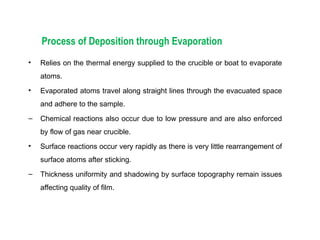
Process of Depositionthrough Evaporation
• Relies on the thermal energy supplied to the crucible or boat to evaporate
atoms.
• Evaporated atoms travel along straight lines through the evacuated space
and adhere to the sample.
– Chemical reactions also occur due to low pressure and are also enforced
by flow of gas near crucible.
• Surface reactions occur very rapidly as there is very little rearrangement of
surface atoms after sticking.
– Thickness uniformity and shadowing by surface topography remain issues
affecting quality of film.
110.
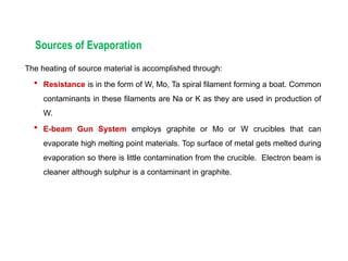
Sources of Evaporation
Theheating of source material is accomplished through:
Resistance is in the form of W, Mo, Ta spiral filament forming a boat. Common
contaminants in these filaments are Na or K as they are used in production of
W.
E-beam Gun System employs graphite or Mo or W crucibles that can
evaporate high melting point materials. Top surface of metal gets melted during
evaporation so there is little contamination from the crucible. Electron beam is
cleaner although sulphur is a contaminant in graphite.
111.
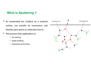
What is Sputtering?
An accelerated ion, incident on a material
surface, can transfer its momentum and
thereby eject atoms or molecules from it.
This process finds applications in
• Dry etching.
• Depth profiling.
• Deposition of thin films.
112.
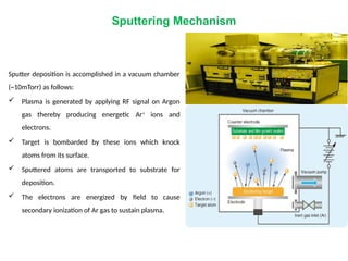
Sputtering Mechanism
Sputter depositionis accomplished in a vacuum chamber
(~10mTorr) as follows:
Plasma is generated by applying RF signal on Argon
gas thereby producing energetic Ar+
ions and
electrons.
Target is bombarded by these ions which knock
atoms from its surface.
Sputtered atoms are transported to substrate for
deposition.
The electrons are energized by field to cause
secondary ionization of Ar gas to sustain plasma.
113.
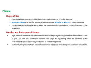
Plasma
Choice of Gas
•Chemically inert gases are chosen for sputtering plasma so as to avoid reactions.
• Argon and Neon are used for light target elements while Krypton or Xenon for heavy elements.
• Efficient momentum transfer occurs when the mass of the sputtering ion is close to the mass of the
target atom.
Creation and Sustenance of Plasma
• High potential difference in excess of breakdown voltage of gas is applied to cause ionization of the
Ar gas. Ar+
ions are accelerated towards the target for sputtering while the electrons suffer
acceleration to cause secondary ionizations to sustain the plasma.
• Sufficiently low pressure helps electrons accelerate repeatedly for subsequent secondary ionizations.
114.
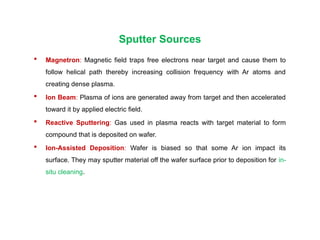
Sputter Sources
Magnetron:Magnetic field traps free electrons near target and cause them to
follow helical path thereby increasing collision frequency with Ar atoms and
creating dense plasma.
Ion Beam: Plasma of ions are generated away from target and then accelerated
toward it by applied electric field.
Reactive Sputtering: Gas used in plasma reacts with target material to form
compound that is deposited on wafer.
Ion-Assisted Deposition: Wafer is biased so that some Ar ion impact its
surface. They may sputter material off the wafer surface prior to deposition for in-
situ cleaning.
115.
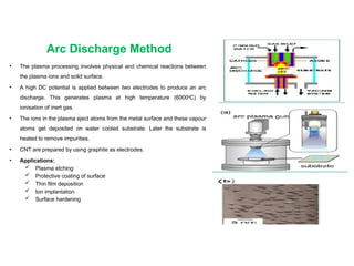
Arc Discharge Method
•The plasma processing involves physical and chemical reactions between
the plasma ions and solid surface.
• A high DC potential is applied between two electrodes to produce an arc
discharge. This generates plasma at high temperature (6000o
C) by
ionisation of inert gas.
• The ions in the plasma eject atoms from the metal surface and these vapour
atoms get deposited on water cooled substrate. Later the substrate is
heated to remove impurities.
• CNT are prepared by using graphite as electrodes.
• Applications:
Plasma etching
Protective coating of surface
Thin film deposition
Ion implantation
Surface hardening
116.
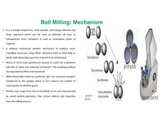
Ball Milling: Mechanism
•It is a simple inexpensive, most popular and energy intensive top
down approach which can be used to fabricate all class of
nanoparticles from crystalline as well as amorphous phase of
material.
• It employs mechanical attrition mechanism to produce nano-
crystalline structures using either refractory balls or steel balls or
plastic balls depending upon the material to be synthesized.
• Macro or micro scale particles are ground in a ball mill, a planetary
ball mill, or other size reducing mechanism. The resulting particles
are separated by filters and recovered.
• When these balls rotate at a particular rpm, the necessary energy is
transferred to the powder which in turn reduces the powder of
coarse grains to ultrafine grains.
• Particle sizes range from tens to hundreds of nm and characterized
by varied particle geometry. May contain defects and impurities
from the milling process.
117.
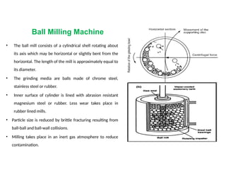
Ball Milling Machine
•The ball mill consists of a cylindrical shell rotating about
its axis which may be horizontal or slightly bent from the
horizontal. The length of the mill is approximately equal to
its diameter.
• The grinding media are balls made of chrome steel,
stainless steel or rubber.
• Inner surface of cylinder is lined with abrasion resistant
magnesium steel or rubber. Less wear takes place in
rubber lined mills.
• Particle size is reduced by brittle fracturing resulting from
ball-ball and ball-wall collisions.
• Milling takes place in an inert gas atmosphere to reduce
contamination.
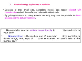
• Because oftheir small size, nanoscale devices can readily interact with
biomolecules on both the surface of cells and inside of cells.
• By gaining access to so many areas of the body, they have the potential to detect
disease and the deliver treatment.
1. Nanotechnology Applications in Medicine
• Nanoparticles can can deliver drugs directly to diseased cells in
your body.
• Nanomedicine is the medical use of molecular- sized particles to
deliver drugs, heat, light or other substances to specific cells in the
human body.
126.
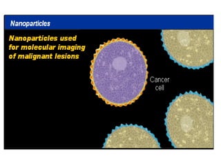
• Quantum dot-that identify the location of cancer cells in the body.
• Nano Particles - that deliver chemotherapy drugs directly to cancer
cells to minimize damage to healthy cells.
• Nanoshells - that concentrate the heat from infrared light to destroy
cancer cells with minimal damage to surrounding healthy cells.
• Nanotubes- used in broken bones to provide a structure for new bone
material to grow.
127.
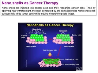
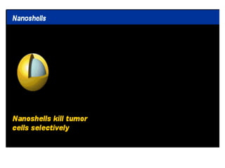
Nano shells asCancer Therapy
Nano shells are injected into cancer area and they recognize cancer cells. Then by
applying near-infrared light, the heat generated by the light-absorbing Nano shells has
successfully killed tumor cells while leaving neighboring cells intact.
130.
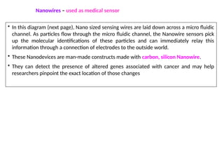
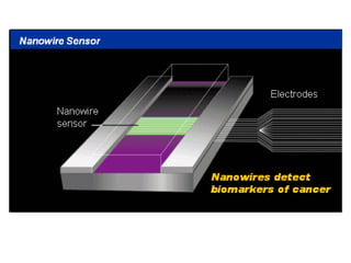
• In thisdiagram (next page), Nano sized sensing wires are laid down across a micro fluidic
channel. As particles flow through the micro fluidic channel, the Nanowire sensors pick
up the molecular identifications of these particles and can immediately relay this
information through a connection of electrodes to the outside world.
• These Nanodevices are man-made constructs made with carbon, silicon Nanowire.
• They can detect the presence of altered genes associated with cancer and may help
researchers pinpoint the exact location of those changes
Nanowires – used as medical sensor
132.
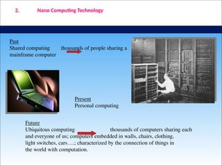
Past
Shared computing thousandsof people sharing a
mainframe computer
Present
Personal computing
Future
Ubiquitous computing thousands of computers sharing each
and everyone of us; computers embedded in walls, chairs, clothing,
light switches, cars….; characterized by the connection of things in
the world with computation.
2. Nano Computing Technology
133.
3. Sunscreens andCosmetics
• Nanosized titanium dioxide and zinc oxide are currently used in some sunscreens, as
they absorb and reflect ultraviolet (UV) rays.
• Nanosized iron oxide is present in some lipsticks as a pigment.
4. Fuel Cells
The potential use of nano-engineered membranes to intensify catalytic processes could
enable higher-efficiency, small-scale fuel cells.
5. Displays
• Nanocrystalline zinc selenide, zinc sulphide, cadmium sulphide and lead telluride are
candidates for the next generation of light-emitting phosphors.
• CNTs are being investigated for low voltage field-emission displays; their strength, sharpness,
conductivity and inertness make them potentially very efficient and long-lasting emitters.
134.
6. Batteries
• Withthe growth in portable electronic equipment (mobile phones, navigation devices,
laptop computers, remote sensors), there is great demand for lightweight, high-energy
density batteries.
• Nanocrystalline materials are candidates for separator plates in batteries because of their
foam-like (aerogel) structure, which can hold considerably more energy than conventional
ones.
• Nickel–metal hydride batteries made of nanocrystalline nickel and metal hydrides are
envisioned to require less frequent recharging and to last longer because of their large
grain boundary (surface) area.
7. Catalysts
In general, nanoparticles have a high surface area, and hence provide higher catalytic activity.
135.
8. Magnetic NanoMaterials applications
• It has been shown that magnets made of nanocrystalline yttrium–samarium–cobalt
grains possess unusual magnetic properties due to their extremely large grain interface
area (high coercivity can be obtained because magnetization flips cannot easily
propagate past the grain boundaries).
• This could lead to applications in motors, analytical instruments like magnetic
resonance imaging (MRI), used widely in hospitals, and microsensors.
• Nanoscale-fabricated magnetic materials also have applications in data storage.
• Devices such as computer hard disks storage capacity is increased with Magnetic Nano
materials
136.
.
• Unfortunately, insome cases, the biomedical metal alloys may wear out within the lifetime
of the patient. But Nano materials increases the life time of the implant materials.
• Nanocrystalline zirconium oxide (zirconia) is hard, wear resistant, bio-corrosion resistant
and bio-compatible.
• It therefore presents an attractive alternative material for implants.
• Nanocrystalline silicon carbide is a candidate material for artificial heart valves primarily
because of its low weight, high strength and inertness.
9. Medical Implantation
10. Water purification
•Nano-engineered membranes could potentially lead to more energy-efficient water
purification processes, notably in desalination process.
137.
11. Military BattleSuits
• Enhanced nanomaterials form the basis of a state-of- the-art ‘battle suit’ that is
being developed.
• A short-term development is likely to be energy-absorbing materials that will
withstand blast waves;
• longer-term are those that incorporate sensors to detect or respond to chemical
and biological weapons (for example, responsive nanopores that ‘close’ upon
detection of a biological agent).
Editor's Notes
#17 Brief History:
The concepts of nanotechnology are not inherently new to nature or to the history of mankind. Science and nature have taught us that biological systems are built using small cells and proteins that follow an intrinsic plan dictated by infinitesimally small genetic coding (Roukes, et al., 2002). A well documented and early example of a manmade nanoprocess is the work of Medieval stained glass makers who used small nanosize gold particles of varying sizes to create the different color hues found in stained glass windows of Medieval churches and structures. Hence, gold particles display a different form of color depending on their size at the nanoscale (Ratner & Ratner, 2003). Gold at the larger scale, the macroscale, such as a gold brick reflects the well known yellowish color.
Fig. 1.7 - http://en.wikipedia.org/wiki/Image:Marcelle-ferron.jpg.
Fig. 1.8 - http://en.wikipedia.org/wiki/Image:Bismuth_crystal_macro.jpg.
#20 Brief History, Continued:
Dr. Richard P. Feynman:
The first well documented talk on the possibilities of nanotechnology was made by one of America’s most notable physicists, Richard Feynman (Zyvex, 2007). Dr. Feynman’s talk was called There Is Plenty of Room at the Bottom, and he delivered it on December 12, 1959, before the American Physical Society meeting held at Caltech. In his talk, Feynman challenged the scientific community to think small in terms of solving future problems. Feynman stated:
“Why cannot we write the entire 24 volumes of the Encyclopedia Britannica on the head of a pin?” (Zyvex, 2007).
Fig. 1.11 - http://en.wikipedia.org/wiki/Image:Feynman_and_Oppenheimer_at_Los_Alamos.jpg.
#21 Brief History, Continued:
Birth of Nanotechology:
In contemporary times, manufacturing tolerances of parts have approached nanometric dimensions, especially in the manufacturing of semiconductor devices. However, the term “nanotechnology” was not coined until 1974 by Professor Norio Taniguchi, whose work and research was in the area of high precision machining (Wikipedia, 2007).
Professor Taniguchi of Tokyo Science University used the word “nanotechnology” to describe the science and technology of processing or building parts with nanometric tolerances. Essentially, Professor Taniguchi’s theoretical concepts involved the use of electron, ion beam, and laser beam processes for machining tolerances at the nanoscale. (Booker & Boysen, 2005).
Fig. 1.9 - http://en.wikipedia.org/wiki/Image:Ridailogo.gif.
Fig. 1.10 – ACC Instructional Development Services.
#22 More History:
Eric Drexler:
Eric Drexler’s book, Engines of Creation, first published in 1986, popularized the futuristic possibilities of nanotechnology. Engines of Creation covered everything from artificial intelligence to self-replicating machines to the use of nanotechnology to cure infectious diseases and repair damaged cells. Drexler also talked about how nanotechnology could be used to extend human lifespan, by placing people in suspended animation when they die so that they can later be brought back to life once a cure was found. Drexler also discussed how humans would be able to populate civilizations away from earth, on near planets or in space stations.
Drexler talked about the dangers of nanotechnology and specifically mentioned the “Grey Goo” phenomena (Drexler, 1986). Grey Goo is the term given to the potential problem of self-replicating and autonomous artificial intelligence machines that can take over the world and wipe out life as we know it today. This is a doomsday theory also called “Ecophagy,” where artificial intelligence machines multiply uncontrollably and spread much like bacteria until they consume all resources of Earth and turn the Earth itself into Grey Goo. Drexler wrote, “Dangerous replicators could easily be too tough, small, and rapidly spreading to stop – at least if we made no preparation” (Drexler, 1986).
Fig. 1.14 – ACC Instructional Development Services.
Fig. 1.15 – http://en.wikipedia.org/wiki/DNA_repair.
#23 Brief History, Continued:
Atomic Scale:
Feynman also discussed how matter at the atomic scale behaves differently than matter at the macroscopic scale since, he mentioned, at the atomic scale atomic size particles respond to forces governed by quantum mechanics as opposed to larger systems which are governed by classical Newtonian mechanics.
Also, the theoretical ability to build new compounds or materials one atom at a time opens up new possibilities beyond those developed using traditional chemical processes. A visual example of this concept is illustrated by a model of a Self Assembling Double Helix of Nano Ice which shows the atoms binding under high pressure with weak hydrogen links (UNL News Releases, 2006).
Fig. 1.13 - http://ucommxsrv1.unl.edu/unlnews2004/downloadables/photo/20061211helix.jpg.