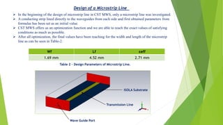
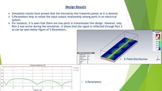
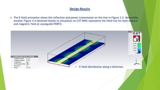
Microstrip Line Design
THEORY OF A MICROSTRIPLINE
➢ The fabrication of microstrip line is handled by photolithographic process and it is easily united
within microwave devices. For this reason, the most well-known kind of planar transmission
line is microstrip line[1].
➢ Field line distributions and basic geometry a microstrip line is depicted in Figure .
A conductor with a width, W, is located on substrate with thickness of ,d, and dielectric
constant, εr [1].
• Microstrip transmission line. (a) Geometry. (b) Electric and magnetic field lines [1].
[1]D. M. Pozar, "MICROSTRIP," in Microwave Engineering, NJ, Wiley, 2005, pp. 143-146.
➢ A hybrid TE-TM wave is being used for the representation of exact field of a microstrip line,
so it requires more advanced examination methods. If the substrate is electrically very thin
(d << λ), the fields become quasi-TEM. It means that the fields are identical as static case.
THEORY OF A MICROSTRIPLINE
➢ Then, expression of phase velocity and propagation constant:
𝝑 𝑷 =
𝒄
𝜺 𝒆
𝜷 = 𝒌 𝟎 𝜺 𝒆
➢ Where εe is the effective relative permittivity of the microstrip line. The effective relative
permittivity constant has to meet the relation: 1 < 𝜺 𝒆 < 𝜺 𝒓 which is related to the substrate
thickness (d) and the conductor width (W) [1].
➢ The effective relative permittivity constant is described as a homogeneous medium which a
replacement of dielectric region of the microstrip and air.
[1]D. M. Pozar, "MICROSTRIP," in Microwave Engineering, NJ, Wiley, 2005, pp. 143-146.
DESING FORMULAS
➢ An effective dielectric constant that describes the air and dielectric region of the microstrip by a
homogenous medium should be defined: 𝜀 𝑒 =
𝜀 𝑟+1
2
+
𝜀 𝑟−1
2
×
1
1+
12𝑑
𝑊
➢ The derivation for characteristic impedance of the microstrip line related to given dimensions:
𝑍0 =
60
𝜀 𝑒
ln
8𝑑
𝑊
+
𝑊
4𝑑
for
𝑊
𝑑
≤ 1 𝑍0 =
120𝜋
𝜀
𝑒
𝑊
𝑑
+1.393+0.667 ln
𝑊
𝑑
+1.444
for
𝑊
𝑑
≥ 1
For relative permittivity constant 𝜀𝑟 and a given characteristic impedance 𝑍0 , 𝑊𝑑 ratio can be calculated as
follow :
8𝑒 𝐴
𝑒2𝐴 − 2
𝑓𝑜𝑟
𝑊
𝑑
< 2
2
𝜋
𝐵 − 1 − ln 2𝐵 − 1 +
𝜀 𝑟 − 1
2𝜀 𝑟
ln 𝐵 − 1 + 0.39 −
0.61
𝜀 𝑟
𝑓𝑜𝑟
𝑊
𝑑
> 2
𝑊
𝑑
=
[1]D. M. Pozar, "MICROSTRIP," in Microwave Engineering, NJ, Wiley, 2005, pp. 143-146.
DESING FORMULAS
Where :
𝐴 =
𝑍0
60
𝜀 𝑟 + 1
2
+
𝜀 𝑟 − 1
𝜀 𝑟 + 1
0.23 +
0.11
2
𝐵 =
377𝜋
2𝑍0 𝜀 𝑟
➢ The attenuation because of the dielectric loss can be
determined as:
𝛼 𝑑 =
𝑘0 𝜀 𝑟(𝜀 𝑒 − 1) tan 𝛿
2 𝜀 𝑒 𝜀 𝑟 − 1
where tan 𝛿 represents the loss tangent of the dielectric.
𝑁𝑝/𝑚
➢ Conductor loss causes attenuation , and it is stated by 𝛼 𝐶 =
𝑅 𝑆
𝑍0 𝑊
𝑁𝑝/𝑚
where 𝑅 𝑆 =
𝜔𝜇0
2𝜎
is the surface resistivity of the conductor [14].
[1]D. M. Pozar, "MICROSTRIP," in Microwave Engineering, NJ, Wiley, 2005, pp. 143-146.
Design of a Microstrip Line
➢ The antenna feeding can be described as a wire or cable which is a connection among the receiver and
transmitter, so it can be imagined like a bridge between the receiver and the transmitter.
➢ There are basically two types of strip line which can be categorized non-conduct or conduct. During
this design project, conducted type is preferred.
➢ In conducted strip line, the radiating patch is fed by RF power directly. Here, between power and
feeding point microstrip line technique has been implemented.
➢ It is a well-known fact that feeding method has a crucial impact on the antenna in terms of
bandwidth, return loss and the performance of antenna efficiency.
➢ Another impact occurs due to substrate thickness. There is a direct relation between the substrate
thickness, d, and surface waves, spurious feeding radiation. These parameters may restrain the
bandwidth of the antenna.
The design process in the beginning, has started based on the given parameters.
● The working frequency is 10 GHz
● The input impedance, Z0, is 50 Ω
● Substrate ISOLA – IS680-345
Design of a Microstrip Line
ISOLA-IS680-345
d =0.76 mm εr = 3.45 dcu =38μm
Table 1 – Parameters of the substrate.
➢ After the implementation of the given parameters into the indicated formulas previously,optimized
parameters for the design process were obtained.
The construction of the model has been done by following steps:
● Set the Units – geometrical units in mm, frequency in GHz.
● Define material for the substrate ISOLA-IS680-345.
● Load Copper from material library
● Define brick for the substrate
● Define brick for the transmission line
● Define brick for the ground plane
● Define Waveguide Port1 and Port2 separately for each end side.
● Define boundary conditions: open
● Define frequency range: 5-12 GHz
● Define monitors: E-field ad H-field
● Transient Solver Settings
➢ In the beginning of the design of microstrip line in CST MWS, only a microstrip line was investigated.
➢ A conducting strip lined directly to the waveguides from each side and first obtained parameters from
formulas has been set as an initial value.
➢ CST MWS offers us an optimization function and we are able to reach the exact values of satisfying
conditions as much as possible.
➢ After all optimization, the final values have been reaching for the width and length of the microstrip
line as can be seen in Table-2.
Design of a Microstrip Line
Wf Lf εeff
1.69 mm 4.52 mm 2.71 mm
Table 2 – Design Parameters of Microstrip Line.
ISOLA Substrate
Transmission Line
Wave Guide Port
Design Results
• E-Field Distribution
• S-Parameters
➢ Simulation results have proved that the microstrip line transmits power as it is desired.
➢ S-Parameters help to relate the input-output relationship among ports in an electrical
system.
➢ For instance, it is seen that there are two ports in transmission line design. However, only
Port 2 was active during the simulation. It shows that the signal is reflected through Port 2
as can be seen below figure of S-Parameters.
• E-field lines at waveguide PORT 2.
• H-field lines at waveguide PORT 2.
Design Results
➢ The E-field animation shows the reflection and power transmission on the line in Figure 3.3. Meanwhile,
another Figure 3.4 obtained thanks to simulation on CST MWS represents the field line for both electric
and magnetic field at waveguide PORT2.
Design Results
• E-field distribution along z-direction.

Microstripline

  • 1.
  • 2.
    THEORY OF AMICROSTRIPLINE ➢ The fabrication of microstrip line is handled by photolithographic process and it is easily united within microwave devices. For this reason, the most well-known kind of planar transmission line is microstrip line[1]. ➢ Field line distributions and basic geometry a microstrip line is depicted in Figure . A conductor with a width, W, is located on substrate with thickness of ,d, and dielectric constant, εr [1]. • Microstrip transmission line. (a) Geometry. (b) Electric and magnetic field lines [1]. [1]D. M. Pozar, "MICROSTRIP," in Microwave Engineering, NJ, Wiley, 2005, pp. 143-146.
  • 3.
    ➢ A hybridTE-TM wave is being used for the representation of exact field of a microstrip line, so it requires more advanced examination methods. If the substrate is electrically very thin (d << λ), the fields become quasi-TEM. It means that the fields are identical as static case. THEORY OF A MICROSTRIPLINE ➢ Then, expression of phase velocity and propagation constant: 𝝑 𝑷 = 𝒄 𝜺 𝒆 𝜷 = 𝒌 𝟎 𝜺 𝒆 ➢ Where εe is the effective relative permittivity of the microstrip line. The effective relative permittivity constant has to meet the relation: 1 < 𝜺 𝒆 < 𝜺 𝒓 which is related to the substrate thickness (d) and the conductor width (W) [1]. ➢ The effective relative permittivity constant is described as a homogeneous medium which a replacement of dielectric region of the microstrip and air. [1]D. M. Pozar, "MICROSTRIP," in Microwave Engineering, NJ, Wiley, 2005, pp. 143-146.
  • 4.
    DESING FORMULAS ➢ Aneffective dielectric constant that describes the air and dielectric region of the microstrip by a homogenous medium should be defined: 𝜀 𝑒 = 𝜀 𝑟+1 2 + 𝜀 𝑟−1 2 × 1 1+ 12𝑑 𝑊 ➢ The derivation for characteristic impedance of the microstrip line related to given dimensions: 𝑍0 = 60 𝜀 𝑒 ln 8𝑑 𝑊 + 𝑊 4𝑑 for 𝑊 𝑑 ≤ 1 𝑍0 = 120𝜋 𝜀 𝑒 𝑊 𝑑 +1.393+0.667 ln 𝑊 𝑑 +1.444 for 𝑊 𝑑 ≥ 1 For relative permittivity constant 𝜀𝑟 and a given characteristic impedance 𝑍0 , 𝑊𝑑 ratio can be calculated as follow : 8𝑒 𝐴 𝑒2𝐴 − 2 𝑓𝑜𝑟 𝑊 𝑑 < 2 2 𝜋 𝐵 − 1 − ln 2𝐵 − 1 + 𝜀 𝑟 − 1 2𝜀 𝑟 ln 𝐵 − 1 + 0.39 − 0.61 𝜀 𝑟 𝑓𝑜𝑟 𝑊 𝑑 > 2 𝑊 𝑑 = [1]D. M. Pozar, "MICROSTRIP," in Microwave Engineering, NJ, Wiley, 2005, pp. 143-146.
  • 5.
    DESING FORMULAS Where : 𝐴= 𝑍0 60 𝜀 𝑟 + 1 2 + 𝜀 𝑟 − 1 𝜀 𝑟 + 1 0.23 + 0.11 2 𝐵 = 377𝜋 2𝑍0 𝜀 𝑟 ➢ The attenuation because of the dielectric loss can be determined as: 𝛼 𝑑 = 𝑘0 𝜀 𝑟(𝜀 𝑒 − 1) tan 𝛿 2 𝜀 𝑒 𝜀 𝑟 − 1 where tan 𝛿 represents the loss tangent of the dielectric. 𝑁𝑝/𝑚 ➢ Conductor loss causes attenuation , and it is stated by 𝛼 𝐶 = 𝑅 𝑆 𝑍0 𝑊 𝑁𝑝/𝑚 where 𝑅 𝑆 = 𝜔𝜇0 2𝜎 is the surface resistivity of the conductor [14]. [1]D. M. Pozar, "MICROSTRIP," in Microwave Engineering, NJ, Wiley, 2005, pp. 143-146.
  • 6.
    Design of aMicrostrip Line ➢ The antenna feeding can be described as a wire or cable which is a connection among the receiver and transmitter, so it can be imagined like a bridge between the receiver and the transmitter. ➢ There are basically two types of strip line which can be categorized non-conduct or conduct. During this design project, conducted type is preferred. ➢ In conducted strip line, the radiating patch is fed by RF power directly. Here, between power and feeding point microstrip line technique has been implemented. ➢ It is a well-known fact that feeding method has a crucial impact on the antenna in terms of bandwidth, return loss and the performance of antenna efficiency. ➢ Another impact occurs due to substrate thickness. There is a direct relation between the substrate thickness, d, and surface waves, spurious feeding radiation. These parameters may restrain the bandwidth of the antenna.
  • 7.
    The design processin the beginning, has started based on the given parameters. ● The working frequency is 10 GHz ● The input impedance, Z0, is 50 Ω ● Substrate ISOLA – IS680-345 Design of a Microstrip Line ISOLA-IS680-345 d =0.76 mm εr = 3.45 dcu =38μm Table 1 – Parameters of the substrate. ➢ After the implementation of the given parameters into the indicated formulas previously,optimized parameters for the design process were obtained. The construction of the model has been done by following steps: ● Set the Units – geometrical units in mm, frequency in GHz. ● Define material for the substrate ISOLA-IS680-345. ● Load Copper from material library ● Define brick for the substrate ● Define brick for the transmission line ● Define brick for the ground plane ● Define Waveguide Port1 and Port2 separately for each end side. ● Define boundary conditions: open ● Define frequency range: 5-12 GHz ● Define monitors: E-field ad H-field ● Transient Solver Settings
  • 8.
    ➢ In thebeginning of the design of microstrip line in CST MWS, only a microstrip line was investigated. ➢ A conducting strip lined directly to the waveguides from each side and first obtained parameters from formulas has been set as an initial value. ➢ CST MWS offers us an optimization function and we are able to reach the exact values of satisfying conditions as much as possible. ➢ After all optimization, the final values have been reaching for the width and length of the microstrip line as can be seen in Table-2. Design of a Microstrip Line Wf Lf εeff 1.69 mm 4.52 mm 2.71 mm Table 2 – Design Parameters of Microstrip Line. ISOLA Substrate Transmission Line Wave Guide Port
  • 9.
    Design Results • E-FieldDistribution • S-Parameters ➢ Simulation results have proved that the microstrip line transmits power as it is desired. ➢ S-Parameters help to relate the input-output relationship among ports in an electrical system. ➢ For instance, it is seen that there are two ports in transmission line design. However, only Port 2 was active during the simulation. It shows that the signal is reflected through Port 2 as can be seen below figure of S-Parameters.
  • 10.
    • E-field linesat waveguide PORT 2. • H-field lines at waveguide PORT 2. Design Results
  • 11.
    ➢ The E-fieldanimation shows the reflection and power transmission on the line in Figure 3.3. Meanwhile, another Figure 3.4 obtained thanks to simulation on CST MWS represents the field line for both electric and magnetic field at waveguide PORT2. Design Results • E-field distribution along z-direction.