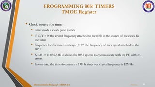
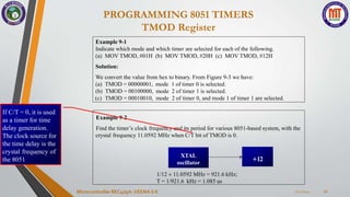
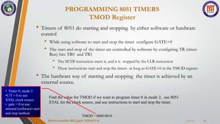
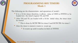
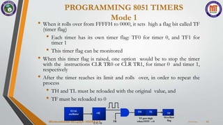
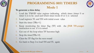
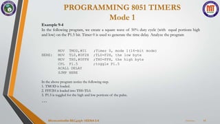
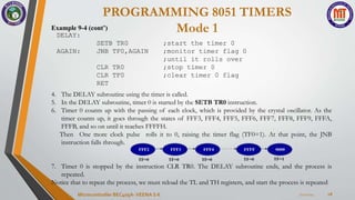
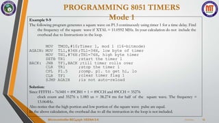
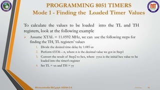
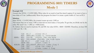
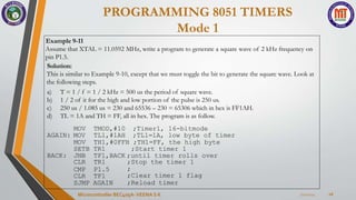
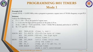
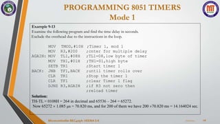
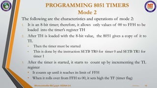
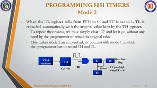
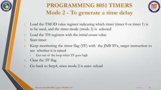
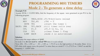
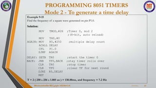
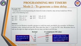
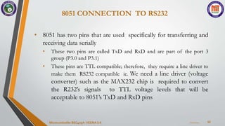
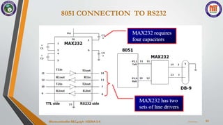
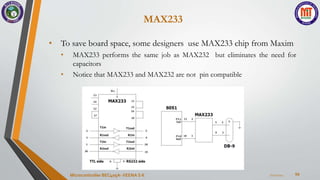
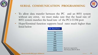
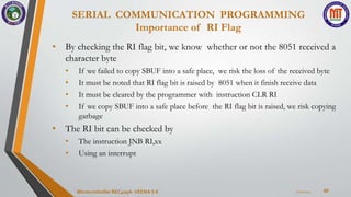
Module 3:
8051 TIMERS & SERIAL PORT
MICROCONTROLLER
VEENA S K
VISION OF THE DEPARTMENT
To be recognized by the society at large as
offering Value based Quality Education to groom
the next generation entrepreneurs, leaders and
researchers in the field of Electronics and
Communication to meet the challenges at global
level.
7/22/2024
Microcontroller BEC405A-VEENA S K 2
MISSION OF THE DEPARTMENT
• To groom the students with strong foundations of Electronics and
Communication Engineering and to facilitate them to pursue higher education
and research.
• To educate and prepare the students to be competent to face the challenges of
the industry/society and /or to become successful entrepreneurs.
• To provide ethical and value-based education by promoting activities addressing
the societal needs.
• Enable students to develop skills to solve complex technological problems of
current times and also provide a framework for promoting collaborative and
multidisciplinary activities.
7/22/2024
Microcontroller BEC405A-VEENA S K 3
Program Educational Objectives (PEOs)
•Be able to have a successful career in dynamic industry that
is global, multidisciplinary, and evolving.
•Solve problems, design and innovate while they work
individually or in teams with sense of professional ethics
and social responsibility.
•Communicate effectively and manage resources skillfully as
members and leaders of the profession
7/22/2024
Microcontroller BEC405A-VEENA S K 4
Program Specific Outcomes (PSOs)
•An ability to apply the basic concepts of engineering
science into various areas of Electronics Communication
Engineering.
•An ability to solve complex Electronics and
Communication Engineering problems, using state of the
art hardware and software tools, along with analytical skills
to arrive at cost effective and efficient solutions.
7/22/2024
Microcontroller BEC405A-VEENA S K 5
Module – 3
Timers/Counters & Serial port programming:
RBT Level
COs
addressed
Basics of Timers & Counters, Data types & Time delay in the 8051 using
C, Programming 8051 Timers, Mode 1 & Mode 2 Programming, Counter
Programming (Assembly Language only). (Text book 2- 3.4, Text book
1- 7.1, 9.1,9.2)
Basics of Serial Communication, 8051 Connection to RS232,
Programming the 8051 to transfer data serially & to receive data serially
using C.( Text book 2- 3.5, Text book 1- 10.1,10.2,10.3 except assembly
language programs, 10.5)
L1,
L2,
L3
CO2,
CO3
7/22/2024
Microcontroller BEC405A-VEENA S K 6
Text Books:
1. “The 8051 Microcontroller and Embedded Systems – using assembly and C”, Muhammad
Ali Mazidi and Janice Gillespie Mazidi and Rollin D. McKinlay; PHI, 2006 / Pearson, 2006.
PROGRAMMING 8051 TIMERS
7
• The 8051 has two timers/counters, they can be used either as
• Timers to generate a time delay or as
• Event counters to count events happening outside the microcontroller
• Both Timer 0 and Timer 1 are of 16 bits
• Since 8051 has an 8-bit architecture, each 16-bits timer is accessed as two
separate registers of low byte and high byte
7/22/2024
Microcontroller BEC405A-VEENA S K
PROGRAMMING 8051 TIMERS
8
• Timer 0 and Timer 1 registers
• low byte register is called TL0/TL1 (Timer 0/1 low byte) and the high byte
register is referred to as TH0 /TH1 (Timer 0/1 high byte)
• can be accessed like any other register, such as A, B, R0, R1, R2, etc.
• Eg:
MOV TL0, #4 FH; moves the value 4FH into TL0
MOV R5, TH0; saves TH0 (high byte of Timer 0) in R5
Figure 1
Timer 0 Registers
Figure 2
Timer 1 Registers
7/22/2024
Microcontroller BEC405A-VEENA S K
PROGRAMMING 8051 TIMERS
TMOD Register
9
TMOD (timer mode) register
• Timers 0 and 1 use TMOD register to set operation modes (only learn Mode 1
and 2)
• TMOD is a 8-bit register
• The lower 4 bits are for Timer 0
• The upper 4 bits are for Timer 1
• In each case,
• The lower 2 bits are used to set the timer mode
• The upper 2 bits to specify the operation
GATE C/T M1 M0
Timer1
GATE C/T M1 M0
Timer0
7/22/2024
Microcontroller BEC405A-VEENA S K
10
Figure 9–3 TMOD Register
PROGRAMMING 8051 TIMERS
TMOD Register
7/22/2024
Microcontroller BEC405A-VEENA S K
11
• Clock source for timer
• timer needs a clock pulse to tick
• if C/T = 0, the crystal frequency attached to the 8051 is the source of the clock for
the timer
• frequency for the timer is always 1/12th the frequency of the crystal attached to the
8051
• XTAL = 11.0592 MHz allows the 8051 system to communicate with the PC with no
errors
• In our case, the timer frequency is 1MHz since our crystal frequency is 12MHz
PROGRAMMING 8051 TIMERS
TMOD Register
7/22/2024
Microcontroller BEC405A-VEENA S K
7/22/2024
Microcontroller BEC405A-VEENA S K 12
Example 9-1
Indicate which mode and which timer are selected for each of the following.
(a) MOV TMOD, #01H (b) MOV TMOD, #20H (c) MOV TMOD, #12H
Solution:
We convert the value from hex to binary. From Figure 9-3 we have:
(a) TMOD = 00000001, mode 1 of timer 0 is selected.
(b) TMOD = 00100000, mode 2 of timer 1 is selected.
(c) TMOD = 00010010, mode 2 of timer 0, and mode 1 of timer 1 are selected.
PROGRAMMING 8051 TIMERS
TMOD Register
Example 9-2
Find the timer’s clock frequency and its period for various 8051-based system, with the
crystal frequency 11.0592 MHz when C/T bit of TMOD is 0.
1/12  11.0592 MHz = 921.6 kHz;
T = 1/921.6 kHz = 1.085 us
XTAL
oscillator
÷12
If C/T = 0, it is used
as a timer for time
delay generation.
The clock source for
the time delay is the
crystal frequency of
the 8051
7/22/2024
Microcontroller BEC405A-VEENA S K 13
PROGRAMMING 8051 TIMERS
TMOD Register
• Timers of 8051 do starting and stopping by either software or hardware
control
• While using software to start and stop the timer configure GATE=0
• The start and stop of the timer are controlled by software by configiring TR (timer
Run) bits TR0 and TR1
• The SETB instruction starts it, and it is stopped by the CLR instruction
• These instructions start and stop the timers as long as GATE=0 in the TMOD register
• The hardware way of starting and stopping the timer is achieved by an
external source.
Find the value for TMOD if we want to program timer 0 in mode 2, use 8051
XTAL for the clock source, and use instructions to start and stop the timer.
TMOD = 0000 0010
• Timer 0, mode 2
•C/T = 0 to use
XTAL clock source
• gate = 0 to use
internal (software) start
and stop method.
7/22/2024
Microcontroller BEC405A-VEENA S K 14
The following are the characteristics and operations of mode1:
• It is a 16-bit timer; therefore, it allows value of 0000 to FFFFH to be
loaded into the timer’s register TL and TH
• After TH and TL are loaded with a 16-bit initial value, the timer must
be started
• This is done by SETB TR0 for timer 0 and SETB TR1 for timer 1
• After the timer is started, it starts to count up
• It counts up until it reaches its limit of FFFFH
PROGRAMMING 8051 TIMERS
Mode 1
PROGRAMMING 8051 TIMERS
Mode 1
7/22/2024
Microcontroller BEC405A-VEENA S K 15
• When it rolls over from FFFFH to 0000, it sets high a flag bit called TF
(timer flag)
• Each timer has its own timer flag: TF0 for timer 0, and TF1 for
timer 1
• This timer flag can be monitored
• When this timer flag is raised, one option would be to stop the timer
with the instructions CLR TR0 or CLR TR1, for timer 0 and timer 1,
respectively
• After the timer reaches its limit and rolls over, in order to repeat the
process
• TH and TL must be reloaded with the original value, and
• TF must be reloaded to 0
XTAL
oscillator TF
Overflow
flag
TH TL
÷12
TF goes high
when FFFF  0
TR
C/T = 0
PROGRAMMING 8051 TIMERS
Mode 1
7/22/2024
Microcontroller BEC405A-VEENA S K 16
To generate a time delay
1. Load the TMOD value register indicating which timer (timer 0 or
timer 1) is to be used and which timer mode (0 or 1) is selected
2. Load registers TL and TH with initial count value
3. Start the timer (TRx=1)
4. Keep monitoring the timer flag (TF) with the JNB TFx,target
instruction to see if it is raised
5. Get out of the loop when TF becomes high
6. Stop the timer(TRx=0)
7. Clear the TF flag for the next round
8. Go back to Step 2 to load TH and TL again
PROGRAMMING 8051 TIMERS
Mode 1
7/22/2024
Microcontroller BEC405A-VEENA S K 17
Example 9-4
In the following program, we create a square wave of 50% duty cycle (with equal portions high
and low) on the P1.5 bit. Timer 0 is used to generate the time delay. Analyze the program
MOV TMOD,#01 ;Timer 0, mode 1(16-bit mode)
HERE: MOV TL0,#0F2H ;TL0=F2H, the low byte
MOV TH0,#0FFH ;TH0=FFH, the high byte
CPL P1.5 ;toggle P1.5
ACALL DELAY
SJMP HERE
In the above program notice the following step.
1. TMOD is loaded.
2. FFF2H is loaded into TH0-TL0.
3. P1.5 is toggled for the high and low portions of the pulse.
…
PROGRAMMING 8051 TIMERS
Mode 1
7/22/2024
Microcontroller BEC405A-VEENA S K 18
Example 9-4 (cont’)
DELAY:
SETB TR0 ;start the timer 0
AGAIN: JNB TF0,AGAIN ;monitor timer flag 0
;until it rolls over
CLR TR0 ;stop timer 0
CLR TF0 ;clear timer 0 flag
RET
4. The DELAY subroutine using the timer is called.
5. In the DELAY subroutine, timer 0 is started by the SETB TR0 instruction.
6. Timer 0 counts up with the passing of each clock, which is provided by the crystal oscillator. As the
timer counts up, it goes through the states of FFF3, FFF4, FFF5, FFF6, FFF7, FFF8, FFF9, FFFA,
FFFB, and so on until it reaches FFFFH.
Then One more clock pulse rolls it to 0, raising the timer flag (TF0=1). At that point, the JNB
instruction falls through.
7. Timer 0 is stopped by the instruction CLR TR0. The DELAY subroutine ends, and the process is
repeated.
Notice that to repeat the process, we must reload the TL and TH registers, and start the process is repeated
PROGRAMMING 8051 TIMERS
Mode 1
7/22/2024
Microcontroller BEC405A-VEENA S K 19
Example 9-5
In Example 9-4, calculate the amount of time delay in the DELAY subroutine generated by
the timer. Assume XTAL = 11.0592 MHz.
Solution:
The timer works with a clock frequency of 1/12 of the XTAL frequency; therefore, we have
11.0592 MHz / 12 = 921.6 kHz as the timer frequency.
As a result, each clock has a period of T = 1/921.6kHz = 1.085us. In other words, Timer 0
counts up each 1.085 us resulting in delay = number of counts x 1.085us.
The number of counts for the roll over is FFFFH – FFF2H = 0DH (13 decimal).
However, we add one to 13 because of the extra clock needed when it rolls over from FFFF to 0
and raise the TF flag. This gives 14 x 1.085us = 15.19us for half the pulse. For the entire period it
is T = 2 x 15.19us = 30.38us as the time delay generated by the timer.
(b) in decimal
Convert YYXX values
of the TH, TL register
to decimal to get a
NNNNN decimal, then
(65536 - NNNN) x
1.085 us
(a) in hex
(FFFF – YYXX + 1) x
1.085 us, where YYXX
are TH, TL initial
values respectively.
Notice that value
YYXX are in hex.
PROGRAMMING 8051 TIMERS
Mode 1
7/22/2024
Microcontroller BEC405A-VEENA S K 20
Example 9-6
In Example 9-5, calculate the frequency of the square wave generated on pin P1.5.
Solution:
In the timer delay calculation of Example 9-5, we did not include the overhead due to instruction in
the loop. To get a more accurate timing, we need to add clock cycles due to this instructions in the
loop. To do that, we use the machine cycle from Table A-1 in Appendix A, as shown below.
Cycles
HERE: MOV
MOV
TL0,#0F2H
TH0,#0FFH
CPL P1.5
ACALL DELAY
SJMP HERE
DELAY:
SETB TR0
AGAIN: JNB TF0,AGAIN
CLR TR0
CLR TF0
RET
2
2
1
2
2
1
14
1
1
2
Total 28
T = 2  28  1.085 us = 60.76 us and F = 16458.2 Hz
PROGRAMMING 8051 TIMERS
Mode 1
7/22/2024
Microcontroller BEC405A-VEENA S K 21
Example 9-7
Find the delay generated by timer 0 in the following code, using both of the Methods of Figure 9-4.
Do not include the overhead due to instruction.
HERE:
AGAIN:
CLR P2.3 ;Clear P2.3
MOV TMOD,#01 ;Timer 0, 16-bitmode
MOV TL0,#3EH ;TL0=3Eh, the low byte
MOV
SETB
TH0,#0B8H ;TH0=B8H, the high byte
P2.3 ;SET high timer 0
SETB
JNB
CLR
TR0 ;Start the timer 0
TF0,AGAIN ;Monitor timer flag 0
TR0 ;Stop the timer 0
CLR TF0 ;Clear TF0 for next round
CLR P2.3
Solution:
a. (FFFFH – B83E + 1) = 47C2H = 18370 in decimal and 18370 x 1.085 us = 19.93145 ms
b. Since TH – TL = B83EH = 47166 (in decimal) we have 65536 – 47166 = 18370. This means that
the timer counts from B83EH to FFFF. This plus Rolling over to 0 goes through a total of 18370
clock cycles, where each clock is 1.085 us in duration.
c. Therefore, we have 18370 x 1.085 us = 19.93145 ms as the width of the pulse.
PROGRAMMING 8051 TIMERS
Mode 1
7/22/2024
Microcontroller BEC405A-VEENA S K 22
Example 9-8
Modify TL and TH in Example 9-7 to get the largest time delay possible. Find the delay in ms. In
your calculation, exclude the overhead due to the instructions in the loop.
Solution:
To get the largest delay we make TL and TH both 0. This will count up from 0000 to FFFFH and then
roll over to zero.
TMOD,#01 ;Timer 0, 16-bitmode
HERE:
CLR P2.3 ;Clear P2.3
MOV
MOV TL0,#0
MOV TH0,#0
SETB P2.3
;TL0=0, the low byte
;TH0=0, the high byte
;SET high P2.3
SETB TR0 ;Start timer 0
AGAIN: JNB TF0,AGAIN ;Monitor timer flag 0
CLR TR0 ;Stop the timer 0
CLR TF0 ;Clear timer 0 flag
CLR P2.3
Making TH and TL both zero means that the timer will count from 0000 to FFFF, and then roll over to
raise the TF flag. As a result, it goes through a total Of 65536 states. Therefore, we have delay =
(65536 - 0) x 1.085 us = 71.1065ms.
PROGRAMMING 8051 TIMERS
Mode 1
7/22/2024
Microcontroller BEC405A-VEENA S K 23
Example 9-9
The following program generates a square wave on P1.5 continuously using timer 1 for a time delay. Find
the frequency of the square wave if XTAL = 11.0592 MHz. In your calculation do not include the
overhead due to Instructions in the loop.
MOV
AGAIN: MOV
TMOD,#10;Timer 1, mod 1 (16-bitmode)
TL1,#34H ;TL1=34H, low byte of timer
MOV TH1,#76H ;TH1=76H, high byte timer
SETB TR1 ;start the timer 1
BACK: JNB TF1,BACK ;till timer rolls over
CLR TR1
CPL P1.5
CLR TF1
SJMP AGAIN
;stop the timer 1
;comp. p1. to get hi, lo
;clear timer flag 1
;is not auto-reload
Solution:
Since FFFFH – 7634H = 89CBH + 1 = 89CCH and 89CCH = 35276
clock count and 35276 x 1.085 us = 38.274 ms for half of the square wave. The frequency =
13.064Hz.
Also notice that the high portion and low portion of the square wave pulse are equal.
In the above calculation, the overhead due to all the instruction in the loop is not included.
PROGRAMMING 8051 TIMERS
Mode 1 - Finding the Loaded Timer Values
7/22/2024
Microcontroller BEC405A-VEENA S K 24
To calculate the values to be loaded into the TL and TH
registers, look at the following example
 Assume XTAL = 11.0592 MHz, we can use the following steps for
finding the TH, TL registers’ values
1. Divide the desired time delay by 1.085 us
2. Perform 65536 – n, where n is the decimal value we got in Step1
3. Convert the result of Step2 to hex, where yyxx is the initial hex value to be
loaded into the timer’s register
4. Set TL = xx and TH = yy
PROGRAMMING 8051 TIMERS
Mode 1
7/22/2024
Microcontroller BEC405A-VEENA S K 25
Example 9-10
Assume that XTAL = 11.0592 MHz. What value do we need to load the timer’s register if we want to have a
time delay of 5 ms (milliseconds)? Show the program for timer 0 to create a pulse width of 5 ms on P2.3.
Solution:
Since XTAL = 11.0592 MHz, the counter counts up every 1.085 us.
This means that out of many 1.085 us intervals we must make a 5 ms pulse. To get that, we divide one by the
other. We need 5 ms / 1.085 us = 4608 clocks.
To Achieve that we need to load into TL and TH the value 65536 – 4608 = EE00H. Therefore, we have TH
= EE and TL = 00.
TMOD,#01 ;Timer 0, 16-bitmode
HERE:
CLR P2.3 ;Clear P2.3
MOV
MOV TL0,#0 ;TL0=0, the low byte
MOV TH0,#0EEH ;TH0=EE, the high byte
CMP P2.3 ;SET high P2.3
SETB TR0 ;Start timer 0
AGAIN: JNB TF0,AGAIN ;Monitor timer flag 0
CLR TR0
CLR TF0
;Stop the timer 0
;Clear timer 0 flag
PROGRAMMING 8051 TIMERS
Mode 1
7/22/2024
Microcontroller BEC405A-VEENA S K 26
Example 9-11
Assume that XTAL = 11.0592 MHz, write a program to generate a square wave of 2 kHz frequency on
pin P1.5.
Solution:
This is similar to Example 9-10, except that we must toggle the bit to generate the square wave. Look at
the following steps.
a) T = 1 / f = 1 / 2 kHz = 500 us the period of square wave.
b) 1 / 2 of it for the high and low portion of the pulse is 250 us.
c) 250 us / 1.085 us = 230 and 65536 – 230 = 65306 which in hex is FF1AH.
d) TL = 1A and TH = FF, all in hex. The program is as follow.
MOV
AGAIN: MOV
TMOD,#10 ;Timer1, 16-bitmode
TL1,#1AH ;TL1=1A, low byte of timer
MOV TH1,#0FFH ;TH1=FF, the high byte
SETB TR1 ;Start timer 1
BACK: JNB TF1,BACK ;until timer rolls over
CLR TR1
CMP P1.5
CLR TF1
SJMP AGAIN
;Stop the timer 1
;
;Clear timer 1 flag
;Reload timer
PROGRAMMING 8051 TIMERS
Mode 1
7/22/2024
Microcontroller BEC405A-VEENA S K 27
Example 9-12
Assume XTAL = 11.0592 MHz, write a program to generate a square wave of 50 kHz frequency on pin P2.3.
Solution:
Look at the following steps.
a) T = 1 / 50 = 20 us, the period of square wave.
b) 1 / 2 of it for the high and low portion of the pulse is 10 us.
c) 10 ms / 1.085 us = 9.216 and 65536 – 9.216 = 65526.784 in decimal, and in hex it is FFF7h.
d) TL = F7 and TH = FF (hex).
TMOD,#10H
TL1,#0F7h
;Timer 1, mod 1
;TL1=00,low byte of timer
MOV
AGAIN: MOV
MOV TH1,#0FFh ;TH1=DC, the high byte
SETB TR1
BACK: JNB
CLR
CMP
TF1,BACK
TR1
P2.3
SJMP AGAIN
;Start timer 1
;until timer rolls over
;Stop the timer 1
;Comp. p2.3 to get hi, lo
;Reload timer
;mode 1 isn’t auto-reload
PROGRAMMING 8051 TIMERS
Mode 1
7/22/2024
Microcontroller BEC405A-VEENA S K 28
Example 9-13
Examine the following program and find the time delay in seconds.
Exclude the overhead due to the instructions in the loop.
MOV TMOD,#10H ;Timer 1, mod 1
MOV R3,#200 ;cnter for multiple delay
AGAIN: MOV TL1,#08H ;TL1=08,low byte of timer
MOV TH1,#01H ;TH1=01,high byte
SETB TR1 ;Start timer 1
BACK: JNB TF1,BACK ;until timer rolls over
CLR TR1 ;Stop the timer 1
CLR TF1 ;clear Timer 1 flag
DJNZ R3,AGAIN ;if R3 not zero then
;reload timer
Solution:
TH-TL = 0108H = 264 in decimal and 65536 – 264 = 65272.
Now 65272  1.085 s = 70.820 ms, and for 200 of them we have 200 70.820 ms = 14.164024 sec.
PROGRAMMING 8051 TIMERS
Mode 2
7/22/2024
Microcontroller BEC405A-VEENA S K 29
The following are the characteristics and operations of mode 2:
1. It is an 8-bit timer; therefore, it allows only values of 00 to FFH to be
loaded into the timer’s register TH
2. After TH is loaded with the 8-bit value, the 8051 gives a copy of it to
TL
• Then the timer must be started
• This is done by the instruction SETB TR0 for timer 0 and SETB TR1 for
timer 1
3. After the timer is started, it starts to count up by incrementing the TL
register
• It counts up until it reaches its limit of FFH
• When it rolls over from FFH to 00, it sets high the TF (timer flag)
PROGRAMMING 8051 TIMERS
Mode 2
7/22/2024
Microcontroller BEC405A-VEENA S K 30
4. When the TL register rolls from FFH to 0 and TF is set to 1, TL is
reloaded automatically with the original value kept by the TH register.
• To repeat the process, we must simply clear TF and let it go without any
need by the programmer to reload the original value
• This makes mode 2 an auto-reload, in contrast with mode 1 in which
the programmer has to reload TH and TL
XTAL
oscillator
÷12
TR
TH
TL
C/T = 0
TF
TF goes high
when FF  0
Overflow
flag
Reload
PROGRAMMING 8051 TIMERS
Mode 2 - To generate a time delay
7/22/2024
Microcontroller BEC405A-VEENA S K 31
1. Load the TMOD value register indicating which timer (timer 0 or timer 1) is
to be used, and the timer mode (mode 2) is selected
2. Load the TH registers with the initial count value
3. Start timer
4. Keep monitoring the timer flag (TF) with the JNB TFx, target instruction to
see whether it is raised
• Get out of the loop when TF goes high
5. Clear the TF flag
6. Go back to Step4, since mode 2 is auto- reload
PROGRAMMING 8051 TIMERS
Mode 2 - To generate a time delay
7/22/2024
Microcontroller BEC405A-VEENA S K 32
Example 9-14
Assume XTAL = 11.0592 MHz, find the frequency of the square wave generated on pin P1.0 in the
following program
MOV
MOV
TMOD,#20H
TH1,#5
;T1/8-bit/auto reload
;TH1 = 5
SETB TR1 ;start the timer 1
BACK: JNB TF1,BACK ;till timer rolls over
CPL P1.0 ;P1.0 to hi, lo
CLR TF1 ;clear Timer 1 flag
SJMP BACK ;mode 2 is auto-reload
Solution:
First notice the target address of SJMP.
In mode 2 we do not need to reload TH since it is auto-reload.
Now (256 - 05) x 1.085 us = 251 x 1.085 us = 272.33 us is the high portion of the pulse. Since it is a
50% duty cycle square wave, the period T is twice that; as a result T = 2 x 272.33 us = 544.67 us and the
frequency = 1.83597 kHz
PROGRAMMING 8051 TIMERS
Mode 2 - To generate a time delay
7/22/2024
Microcontroller BEC405A-VEENA S K 33
Example 9-15
Find the frequency of a square wave generated on pin P1.0.
Solution:
MOV TMOD,#2H ;Timer 0, mod 2
;(8-bit, auto reload)
MOV
AGAIN: MOV
TH0,#0
R5,#250 ;multiple delay count
ACALL DELAY
CPL P1.0
SJMP AGAIN
DELAY: SETB TR0 ;start the timer 0
BACK: JNB TF0,BACK ;stay timer rolls over
CLR TR0 ;stop timer
CLR TF0 ;clear TF for next round
DJNZ R5,DELAY
RET
T = 2 ( 250 x 256 x 1.085 us ) = 138.88ms, and frequency = 7.2 Hz
PROGRAMMING 8051 TIMERS
Mode 2 - To generate a time delay
7/22/2024
Microcontroller BEC405A-VEENA S K 34
Example 9-16
Assuming that we are programming the timers for mode 2, find the value (in hex) loaded into TH for
each of the following cases.
(a)
(c)
(e)
MOV TH1,#-200 (b) MOV TH0,#-60
MOV TH1,#-3 (d) MOV TH1,#-12
MOV TH0,#-48
Solution:
You can use the Windows scientific calculator to verify the result provided by the assembler. In Windows
calculator, select decimal and enter 200. Then select hex, then +/- to get the TH value. Remember that we
only use the right two digits and ignore the rest since our data is an 8-bit data.
Decimal 2’s complement (TH value)
-3 FDH
-12 F4H
-48
-60
-200
D0H
C4H
38H
The advantage of using
negative values is that you
don’t need to calculate the
value loaded to THx
The number 200 is the
timer count till the TF
is set to 1
7/22/2024
Microcontroller BEC405A- VEENA S K 35
SERIALCOMMUNICATION
BASICS OF SERIAL COMMUNICATION
36
 Computers transfer data in two ways:
 Parallel
 Often 8 or more lines (wire conductors) are used to transfer data to a device that is
only a few feet away
 Serial
 To transfer to a device located many meters away, the serial method is used
 The data is sent one bit at a time
Serial Transfer Parallel Transfer
7/22/2024
Microcontroller BEC405A-VEENA S K
Sender Receiver Sender Receiver
D0
D7
BASICS OF SERIAL COMMUNICATION
37
• At the transmitting end, the byte of data must be converted to serial
bits using parallel-in-serial-out shift register
• At the receiving end, there is a serial-in-parallel-out shift register to
receive the serial data and pack them into byte
• When the distance is short, the digital signal can be transferred as it
is on a simple wire and requires no modulation
• If data is to be transferred on the telephone line, it must be converted
from 0s and 1s to audio tones
• This conversion is performed by a device called a modem,
“Modulator/demodulator”
7/22/2024
Microcontroller BEC405A-VEENA S K
BASICS OF SERIAL COMMUNICATION
38
• Serial data communication uses two methods
• Synchronous method transfers a block of data at a time
• Asynchronous method transfers a single byte at a time
• It is possible to write software to use either of these methods,
but the programs can be tedious and long
• There are special IC chips made by many manufacturers for serial
communications
• UART (universal asynchronous Receiver- transmitter)
• USART (universal synchronous-asynchronous Receiver-transmitter)
7/22/2024
Microcontroller BEC405A-VEENA S K
Simplex, Half- and Full- Duplex Transmission
39
• If data can be transmitted and received(one way), it is a Simplex transmission
(computer and a keyboard, radio station)
• If data transmitted one way a time, it is referred to as half duplex(walkie-talkie)
• If data can go both ways at a time, it is full duplex(telephone)
• This is contrast to simplex transmission
7/22/2024
Microcontroller BEC405A-VEENA S K
Receiver
Transmitter
Transmitter
Receiver
Transmitter
Receiver
Receiver
Simplex
Transmitter
Receiver
Half Duplex
Full Duplex
Transmitter
Receiver
Transmitter
40
• A protocol is a set of rules agreed by both the sender and receiver on
• How the data is packed
• How many bits constitute a character
• When the data begins and ends
• Asynchronous serial data communication is widely used for
character-oriented transmissions
• Each character is placed in between start and stop bits, this is called framing
• The start bit is always one bit, but the stop bit can be one or two bits
• The start bit is always a 0 (low) and the stop bit(s) is 1 (high)
7/22/2024
Microcontroller BEC405A-VEENA S K
Asynchronous Method
Start and Stop Bits
41
7/22/2024
Microcontroller BEC405A-VEENA S K
ASCII character “A” (8-bit binary 0100 0001)
When there is no
transfer, the signal is 1
(high), which is referred
to as mark
The 0 (low) is referred
to as space The transmission begins with a start
bit followed by D0, the LSB, then the
rest of the bits
until MSB (D7), and finally, the one
stop bit indicating the
end of the character
Space
Stop
Bit
0 0 0 0 0 0
1 1
D7 D0
Mark
Start
Bit
Goes out first
Goes out last
42
• Due to the extended ASCII characters, 8-bit ASCII data is common
• In older systems, ASCII characters were 7- bit
• In modern PCs the use of one stop bit is standard
• In older systems, due to the slowness of the receiving mechanical device, two
stop bits were used to give the device sufficient time to organize itself before
transmission of the next byte
• Assuming that we are transferring a text file of ASCII characters
using 1 stop bit, we have a total of 10 bits for each character
• This gives 25% overhead, i.e. each 8-bit character with an extra 2 bits
• In some systems in order to maintain data integrity, the parity bit of
the character byte is included in the data frame
• UART chips allow programming of the parity bit for odd-, even-, and no-
parity options
7/22/2024
Microcontroller BEC405A-VEENA S K
synchronous Method
• Block-oriented data transfers use the synchronous method.
• Recevier and transmitter are synchronized by common clock signal.
• There are no start and stop bits but syncrhronous bits are inserted .
7/22/2024
Microcontroller BEC405A-VEENA S K 43
Data Transfer Rate
44
• The rate of data transfer in serial data communication is stated
in bps (bits per second)
• Another widely used terminology for bps is baud rate
• It is modem terminology and is defined as the number of signal
changes per second
• In modems, there are occasions when a single change of signal
transfers several bits of data
• As far as the conductor wire is concerned, the baud rate and bps
are the same, and we use the terms interchangeably
7/22/2024
Microcontroller BEC405A-VEENA S K
Data Transfer Rate
45
• The data transfer rate of given computer system depends on
communication ports incorporated into that system
• IBM PC/XT could transfer data at the rate of 100 to 9600 bps
• Pentium-based PCs transfer data at rates as high as 56K bps
• In asynchronous serial data communication, the baud rate is limited to
100K bps
7/22/2024
Microcontroller BEC405A-VEENA S K
RS232 Standards
46
• An interfacing standard RS232 was set by the Electronics
Industries Association (EIA) in 1960
• The standard was set long before the advent of the TTL logic
family, its input and output voltage levels are not TTL
compatible
• In RS232, a bit 1 and is represented by -3 ~ -25 V, while a 0 bit
is +3 ~ +25 V, making -3 to +3 undefined
7/22/2024
Microcontroller BEC405A-VEENA S K
RS232 Standards
47
7/22/2024
Microcontroller BEC405A-VEENA S K
RS232 DB-25 Pins
Pin Description Pin Description
1 Protective ground 14 Secondary transmitted data
2 Transmitted data (TxD) 15 Transmitted signal element timing
3 Received data (RxD) 16 Secondary receive data
4 Request to send (-RTS) 17 Receive signal element timing
5 Clear to send (-CTS) 18 Unassigned
6 Data set ready (-DSR) 19 Secondary receive data
7 Signal ground (GND) 20 Data terminal ready (-DTR)
8 Data carrier detect (-DCD) 21 Signal quality detector
9/10 Reserved for data testing 22 Ring indicator (RI)
11 Unassigned 23 Data signal rate select
12 Secondary data carrier detect 24 Transmit signal element timing
13 Secondary clear to send 25 Unassigned
RS232 Connector DB-25
DB-9 RS232 Standards
48
• Since not all pins are used in PC cables, IBM introduced the
DB-9 version of the serial I/O standard
7/22/2024
Microcontroller BEC405A-VEENA S K
RS232 Connector DB-9
Pin Description
1 Data carrier detect (-DCD)
2 Received data (RxD)
3 Transmitted data (TxD)
4 Data terminal ready (DTR)
5 Signal ground (GND)
6 Data set ready (-DSR)
7 Request to send (-RTS)
8 Clear to send (-CTS)
9 Ring indicator (RI)
RS232 DB-9 Pins
DB-9 RS232 Pins
49
• DCD (data carrier detect)
• The modem asserts signal DCD to inform the DTE that a valid carrier
has been detected and that contact between it and the other modem is
established
• RI (ring indicator)
• An output from the modem and an input to a PC indicates that the
telephone is ringing
• It goes on and off in synchronous with the ringing sound
7/22/2024
Microcontroller BEC405A-VEENA S K
DB-9 RS232 Pins
50
• DTR (data terminal ready)
• When terminal is turned on, it sends out signal DTR to indicate that it is
ready for communication
• DSR (data set ready)
• When DCE is turned on and has gone through the self-test, it assert DSR to
indicate that it is ready to communicate
• RTS (request to send)
• When the DTE device has byte to transmit, it assert RTS to signal the
modem that it has a byte of data to transmit
• CTS (clear to send)
• When the modem has room for storing the data it is to receive, it sends out
signal CTS to DTE to indicate that it can receive the data now
7/22/2024
Microcontroller BEC405A-VEENA S K
Data Communication Classification
51
• Current terminology classifies data communication equipment as
• DTE (Data Terminal Equipment) refers to terminal and computers that send
and receive data
• DCE (Data Communication Eequipment) refers to communication
equipment, such as modems
• The simplest connection between a PC and microcontroller requires
a minimum of three pins, TxD, RxD, and ground
7/22/2024
Microcontroller BEC405A-VEENA S K
DTE
TxD
RxD
DTE
TxD
RxD
ground
Null modem connection
8051 CONNECTION TO RS232
52
• 8051 has two pins that are used specifically for transferring and
receiving data serially
• These two pins are called TxD and RxD and are part of the port 3
group (P3.0 and P3.1)
• These pins are TTL compatible; therefore, they require a line driver to
make them RS232 compatible ie. We need a line driver (voltage
converter) such as the MAX232 chip is required to convert
the R232’s signals to TTL voltage levels that will be
acceptable to 8051’s TxD and RxD pins
7/22/2024
Microcontroller BEC405A-VEENA S K
8051 CONNECTION TO RS232
53
7/22/2024
Microcontroller BEC405A-VEENA S K
MAX233
54
• To save board space, some designers use MAX233 chip from Maxim
• MAX233 performs the same job as MAX232 but eliminates the need for
capacitors
• Notice that MAX233 and MAX232 are not pin compatible
7/22/2024
Microcontroller BEC405A-VEENA S K
SERIAL COMMUNICATION PROGRAMMING
55
• To allow data transfer between the PC and an 8051 system
without any error, we must make sure that the baud rate of
8051 system matches the baud rate of the PC’s COM port
• HyperTerminal function supports baud rates much higher than
listed below
7/22/2024
Microcontroller BEC405A-VEENA S K
75
150
300
600
1200
2400
4800
9600
19200
PC Baud Rates
Baud rates supported by
486/Pentium IBM PC BIOS
SERIAL COMMUNICATION PROGRAMMING
SBUF Register
56
• SBUF is an 8-bit register used solely for serial communication
• For a byte data to be transferred via the TxD line, it must be placed in
the SBUF register
• The moment a byte is written into SBUF, it is framed with the start and
stop bits and transferred serially via the TxD line
• SBUF holds the byte of data when it is received by 8051 RxD line
• When the bits are received serially via RxD, the 8051 de-frames it by
eliminating the stop and start bits, making a byte out of the data received,
and then placing it in SBUF
7/22/2024
Microcontroller BEC405A-VEENA S K
MOV SBUF,#’D’ ;load SBUF=44h, ASCII for ‘D’
MOV SBUF,A ;copy accumulator into SBUF
MOV A,SBUF ;copy SBUF into accumulator
SERIAL COMMUNICATION PROGRAMMING
SCON Register
57
• SCON is an 8-bit register used to program the start bit, stop bit,
and data bits of data framing, among other things
7/22/2024
Microcontroller BEC405A-VEENA S K
SM0 SCON.7
SM1 SCON.6
SM2 SCON.5
REN SCON.4
TB8 SCON.3
RB8 SCON.2
TI SCON.1
RI SCON.0
Serial port mode specifier
Used for multiprocessor communication
Set/cleared by software to enable/disable reception
Not widely used
Not widely used
Transmit interrupt flag. Set by HW at the
begin of the stop bit mode 1. And cleared by SW
Receive interrupt flag. Set by HW at the
begin of the stop bit mode 1. And cleared by SW
Note: Make SM2, TB8, and RB8 =0
SM0 SM1 SM2 REN TB8 RB8 TI RI
SERIAL COMMUNICATION PROGRAMMING
SCON Register
58
SM0, SM1
• They determine the framing of data by specifying the number of
bits per character, and the start and stop bits
SM2
• This enables the multiprocessing capability of the 8051
7/22/2024
Microcontroller BEC405A-VEENA S K
SERIAL COMMUNICATION PROGRAMMING
SCON Register
59
REN (receive enable)
• It is a bit-addressable register
• When it is high, it allows 8051 to receive data on RxD pin
• If low, the receiver is disable
TI (transmit interrupt)
• When 8051 finishes the transfer of 8-bit character
• It raises TI flag to indicate that it is ready to transfer another byte
• TI bit is raised at the beginning of the stop bit
RI (receive interrupt)
• When 8051 receives data serially via RxD, it gets rid of the start and stop bits and
places the byte in SBUF register
• It raises the RI flag bit to indicate that a byte has been received and should be
picked up before it is lost
• RI is raised halfway through the stop bit
7/22/2024
Microcontroller BEC405A-VEENA S K
SERIAL COMMUNICATION PROGRAMMING
Programming Serial Data Transmitting
60
In programming the 8051 to transfer character bytes serially
1. TMOD register is loaded with the value 20H, indicating the use of timer 1 in
mode 2 (8-bit auto-reload) to set baud rate
2. The TH1 is loaded with one of the values to set baud rate for serial data
transfer
3. The SCON register is loaded with the value 50H, indicating serial mode 1,
where an 8-bit data is framed with start and stop bits
4. TR1 is set to 1 to start timer 1
5. TI is cleared by CLR TI instruction
6. The character byte to be transferred serially is written into SBUF register
7. The TI flag bit is monitored with the use of instruction JNB TI,xx to see if
the character has been transferred completely
8. To transfer the next byte, go to step 5
7/22/2024
Microcontroller BEC405A-VEENA S K
SERIAL COMMUNICATION PROGRAMMING
Programming Serial Data Transmitting
61
7/22/2024
Microcontroller BEC405A-VEENA S K
Write a program for the 8051 to transfer letter “A” serially at 4800 baud,
continuously.
Solution:
MOV TMOD,#20H ;timer 1,mode 2(auto reload)
MOV TH1,#-6 ;4800 baud rate
MOV SCON,#50H ;8-bit, 1 stop, REN enabled
SETB TR1 ;start timer 1
AGAIN: MOV SBUF,#”A” ;letter “A” to transfer
HERE: JNB TI,HERE ;wait for the last bit
CLR TI ;clear TI for next char
SJMP AGAIN ;keep sending A
SERIAL COMMUNICATION PROGRAMMING
Programming Serial Data Transmitting
62
7/22/2024
Microcontroller BEC405A-VEENA S K
Write a program for the 8051 to transfer “YES” serially at 9600 baud, 8-bit
data, 1 stop bit, do this continuously
Solution:
MOV TMOD,#20H ;timer 1,mode 2(auto reload)
MOV TH1,#-3 ;9600 baud rate
MOV SCON,#50H ;8-bit, 1 stop, REN enabled
SETB TR1 ;start timer 1
;transfer “Y”
AGAIN: MOV A,#”Y”
ACALL TRANS
MOV A,#”E” ;transfer “E”
;transfer “S”
ACALL TRANS
MOV A,#”S”
ACALL TRANS
SJMP AGAIN ;keep doing it
;serial data transfer subroutine
TRANS: MOV
HERE:
;load SBUF
;wait for the last bit
;get ready for next byte
SBUF,A
JNB TI,HERE
CLR TI
RET
SERIAL COMMUNICATION PROGRAMMING
Importance of TI Flag
63
The steps that 8051 goes through in transmitting a character via TxD
1. The byte character to be transmitted is written into the SBUF register
2. The start bit is transferred
3. The 8-bit character is transferred on bit at a time
4. The stop bit is transferred
• It is during the transfer of the stop bit that 8051 raises the TI flag, indicating that
the last character was transmitted
5. By monitoring the TI flag, we make sure that we are not overloading
the SBUF
• If we write another byte into the SBUF before TI is raised, the untransmitted
portion of the previous byte will be lost
6. After SBUF is loaded with a new byte, the TI flag bit must be forced to
0 by CLR TI in order for this new byte to be transferred
7/22/2024
Microcontroller BEC405A-VEENA S K
SERIAL COMMUNICATION PROGRAMMING
Importance of TI Flag
64
• By checking the TI flag bit, we know whether or not the 8051 is
ready to transfer another byte
• It must be noted that TI flag bit is raised by 8051 itself when it finishes
data transfer
• It must be cleared by the programmer with instruction CLR TI
• If we write a byte into SBUF before the TI flag bit is raised, we risk the
loss of a portion of the byte being transferred
• The TI bit can be checked by
• The instruction JNB TI,xx
• Using an interrupt
7/22/2024
Microcontroller BEC405A-VEENA S K
SERIAL COMMUNICATION PROGRAMMING
Programming Serial Data Receiving
65
In programming the 8051 to receive character bytes serially
1. TMOD register is loaded with the value 20H, indicating the use of timer
1 in mode 2 (8-bit auto-reload) to set baud rate
2. TH1 is loaded to set baud rate
3. The SCON register is loaded with the value 50H, indicating serial mode
1, where an 8- bit data is framed with start and stop bits
4. TR1 is set to 1 to start timer 1
5. RI is cleared by CLR RI instruction
6. The RI flag bit is monitored with the use of instruction JNB RI,xx to
see if an entire character has been received yet
7. When RI is raised, SBUF has the byte, its contents are moved into a safe
place
8. To receive the next character, go to step 5
7/22/2024
Microcontroller BEC405A-VEENA S K
SERIAL COMMUNICATION PROGRAMMING
Importance of RI Flag
66
In receiving bit via its RxD pin, 8051 goes through the following steps
• It receives the start bit
• Indicating that the next bit is the first bit of the character byte it is about
to receive
• The 8-bit character is received one bit at time
• The stop bit is received
• When receiving the stop bit 8051 makes RI = 1, indicating that an entire
character byte has been received and must be picked up before it gets
overwritten by an incoming character
7/22/2024
Microcontroller BEC405A-VEENA S K
SERIAL COMMUNICATION PROGRAMMING
Importance of RI Flag
67
(cont’)
• By checking the RI flag bit when it is raised, we know that a
character has been received and is sitting in the SBUF register
• We copy the SBUF contents to a safe place in some other register or
memory before it is lost
• After the SBUF contents are copied into a safe place, the RI flag
bit must be forced to 0 by CLR RI in order to allow the next
received character byte to be placed in SBUF
• Failure to do this causes loss of the received character
7/22/2024
Microcontroller BEC405A-VEENA S K
SERIAL COMMUNICATION PROGRAMMING
Importance of RI Flag
68
• By checking the RI flag bit, we know whether or not the 8051 received a
character byte
• If we failed to copy SBUF into a safe place, we risk the loss of the received byte
• It must be noted that RI flag bit is raised by 8051 when it finish receive data
• It must be cleared by the programmer with instruction CLR RI
• If we copy SBUF into a safe place before the RI flag bit is raised, we risk copying
garbage
• The RI bit can be checked by
• The instruction JNB RI,xx
• Using an interrupt
7/22/2024
Microcontroller BEC405A-VEENA S K
SERIAL COMMUNICATION
PROGRAMMING in C
7/22/2024
Microcontroller BEC405A-VEENA S K 69
The0dore Roosevelt
7/22/2024
Microcontroller BEC405A- VEENA S K 70

Microcontroller BEC405A-Timers and serial communication Module3.pptx

  • 1.
    Module 3: 8051 TIMERS& SERIAL PORT MICROCONTROLLER VEENA S K
  • 2.
    VISION OF THEDEPARTMENT To be recognized by the society at large as offering Value based Quality Education to groom the next generation entrepreneurs, leaders and researchers in the field of Electronics and Communication to meet the challenges at global level. 7/22/2024 Microcontroller BEC405A-VEENA S K 2
  • 3.
    MISSION OF THEDEPARTMENT • To groom the students with strong foundations of Electronics and Communication Engineering and to facilitate them to pursue higher education and research. • To educate and prepare the students to be competent to face the challenges of the industry/society and /or to become successful entrepreneurs. • To provide ethical and value-based education by promoting activities addressing the societal needs. • Enable students to develop skills to solve complex technological problems of current times and also provide a framework for promoting collaborative and multidisciplinary activities. 7/22/2024 Microcontroller BEC405A-VEENA S K 3
  • 4.
    Program Educational Objectives(PEOs) •Be able to have a successful career in dynamic industry that is global, multidisciplinary, and evolving. •Solve problems, design and innovate while they work individually or in teams with sense of professional ethics and social responsibility. •Communicate effectively and manage resources skillfully as members and leaders of the profession 7/22/2024 Microcontroller BEC405A-VEENA S K 4
  • 5.
    Program Specific Outcomes(PSOs) •An ability to apply the basic concepts of engineering science into various areas of Electronics Communication Engineering. •An ability to solve complex Electronics and Communication Engineering problems, using state of the art hardware and software tools, along with analytical skills to arrive at cost effective and efficient solutions. 7/22/2024 Microcontroller BEC405A-VEENA S K 5
  • 6.
    Module – 3 Timers/Counters& Serial port programming: RBT Level COs addressed Basics of Timers & Counters, Data types & Time delay in the 8051 using C, Programming 8051 Timers, Mode 1 & Mode 2 Programming, Counter Programming (Assembly Language only). (Text book 2- 3.4, Text book 1- 7.1, 9.1,9.2) Basics of Serial Communication, 8051 Connection to RS232, Programming the 8051 to transfer data serially & to receive data serially using C.( Text book 2- 3.5, Text book 1- 10.1,10.2,10.3 except assembly language programs, 10.5) L1, L2, L3 CO2, CO3 7/22/2024 Microcontroller BEC405A-VEENA S K 6 Text Books: 1. “The 8051 Microcontroller and Embedded Systems – using assembly and C”, Muhammad Ali Mazidi and Janice Gillespie Mazidi and Rollin D. McKinlay; PHI, 2006 / Pearson, 2006.
  • 7.
    PROGRAMMING 8051 TIMERS 7 •The 8051 has two timers/counters, they can be used either as • Timers to generate a time delay or as • Event counters to count events happening outside the microcontroller • Both Timer 0 and Timer 1 are of 16 bits • Since 8051 has an 8-bit architecture, each 16-bits timer is accessed as two separate registers of low byte and high byte 7/22/2024 Microcontroller BEC405A-VEENA S K
  • 8.
    PROGRAMMING 8051 TIMERS 8 •Timer 0 and Timer 1 registers • low byte register is called TL0/TL1 (Timer 0/1 low byte) and the high byte register is referred to as TH0 /TH1 (Timer 0/1 high byte) • can be accessed like any other register, such as A, B, R0, R1, R2, etc. • Eg: MOV TL0, #4 FH; moves the value 4FH into TL0 MOV R5, TH0; saves TH0 (high byte of Timer 0) in R5 Figure 1 Timer 0 Registers Figure 2 Timer 1 Registers 7/22/2024 Microcontroller BEC405A-VEENA S K
  • 9.
    PROGRAMMING 8051 TIMERS TMODRegister 9 TMOD (timer mode) register • Timers 0 and 1 use TMOD register to set operation modes (only learn Mode 1 and 2) • TMOD is a 8-bit register • The lower 4 bits are for Timer 0 • The upper 4 bits are for Timer 1 • In each case, • The lower 2 bits are used to set the timer mode • The upper 2 bits to specify the operation GATE C/T M1 M0 Timer1 GATE C/T M1 M0 Timer0 7/22/2024 Microcontroller BEC405A-VEENA S K
  • 10.
    10 Figure 9–3 TMODRegister PROGRAMMING 8051 TIMERS TMOD Register 7/22/2024 Microcontroller BEC405A-VEENA S K
  • 11.
    11 • Clock sourcefor timer • timer needs a clock pulse to tick • if C/T = 0, the crystal frequency attached to the 8051 is the source of the clock for the timer • frequency for the timer is always 1/12th the frequency of the crystal attached to the 8051 • XTAL = 11.0592 MHz allows the 8051 system to communicate with the PC with no errors • In our case, the timer frequency is 1MHz since our crystal frequency is 12MHz PROGRAMMING 8051 TIMERS TMOD Register 7/22/2024 Microcontroller BEC405A-VEENA S K
  • 12.
    7/22/2024 Microcontroller BEC405A-VEENA SK 12 Example 9-1 Indicate which mode and which timer are selected for each of the following. (a) MOV TMOD, #01H (b) MOV TMOD, #20H (c) MOV TMOD, #12H Solution: We convert the value from hex to binary. From Figure 9-3 we have: (a) TMOD = 00000001, mode 1 of timer 0 is selected. (b) TMOD = 00100000, mode 2 of timer 1 is selected. (c) TMOD = 00010010, mode 2 of timer 0, and mode 1 of timer 1 are selected. PROGRAMMING 8051 TIMERS TMOD Register Example 9-2 Find the timer’s clock frequency and its period for various 8051-based system, with the crystal frequency 11.0592 MHz when C/T bit of TMOD is 0. 1/12  11.0592 MHz = 921.6 kHz; T = 1/921.6 kHz = 1.085 us XTAL oscillator ÷12 If C/T = 0, it is used as a timer for time delay generation. The clock source for the time delay is the crystal frequency of the 8051
  • 13.
    7/22/2024 Microcontroller BEC405A-VEENA SK 13 PROGRAMMING 8051 TIMERS TMOD Register • Timers of 8051 do starting and stopping by either software or hardware control • While using software to start and stop the timer configure GATE=0 • The start and stop of the timer are controlled by software by configiring TR (timer Run) bits TR0 and TR1 • The SETB instruction starts it, and it is stopped by the CLR instruction • These instructions start and stop the timers as long as GATE=0 in the TMOD register • The hardware way of starting and stopping the timer is achieved by an external source. Find the value for TMOD if we want to program timer 0 in mode 2, use 8051 XTAL for the clock source, and use instructions to start and stop the timer. TMOD = 0000 0010 • Timer 0, mode 2 •C/T = 0 to use XTAL clock source • gate = 0 to use internal (software) start and stop method.
  • 14.
    7/22/2024 Microcontroller BEC405A-VEENA SK 14 The following are the characteristics and operations of mode1: • It is a 16-bit timer; therefore, it allows value of 0000 to FFFFH to be loaded into the timer’s register TL and TH • After TH and TL are loaded with a 16-bit initial value, the timer must be started • This is done by SETB TR0 for timer 0 and SETB TR1 for timer 1 • After the timer is started, it starts to count up • It counts up until it reaches its limit of FFFFH PROGRAMMING 8051 TIMERS Mode 1
  • 15.
    PROGRAMMING 8051 TIMERS Mode1 7/22/2024 Microcontroller BEC405A-VEENA S K 15 • When it rolls over from FFFFH to 0000, it sets high a flag bit called TF (timer flag) • Each timer has its own timer flag: TF0 for timer 0, and TF1 for timer 1 • This timer flag can be monitored • When this timer flag is raised, one option would be to stop the timer with the instructions CLR TR0 or CLR TR1, for timer 0 and timer 1, respectively • After the timer reaches its limit and rolls over, in order to repeat the process • TH and TL must be reloaded with the original value, and • TF must be reloaded to 0 XTAL oscillator TF Overflow flag TH TL ÷12 TF goes high when FFFF  0 TR C/T = 0
  • 16.
    PROGRAMMING 8051 TIMERS Mode1 7/22/2024 Microcontroller BEC405A-VEENA S K 16 To generate a time delay 1. Load the TMOD value register indicating which timer (timer 0 or timer 1) is to be used and which timer mode (0 or 1) is selected 2. Load registers TL and TH with initial count value 3. Start the timer (TRx=1) 4. Keep monitoring the timer flag (TF) with the JNB TFx,target instruction to see if it is raised 5. Get out of the loop when TF becomes high 6. Stop the timer(TRx=0) 7. Clear the TF flag for the next round 8. Go back to Step 2 to load TH and TL again
  • 17.
    PROGRAMMING 8051 TIMERS Mode1 7/22/2024 Microcontroller BEC405A-VEENA S K 17 Example 9-4 In the following program, we create a square wave of 50% duty cycle (with equal portions high and low) on the P1.5 bit. Timer 0 is used to generate the time delay. Analyze the program MOV TMOD,#01 ;Timer 0, mode 1(16-bit mode) HERE: MOV TL0,#0F2H ;TL0=F2H, the low byte MOV TH0,#0FFH ;TH0=FFH, the high byte CPL P1.5 ;toggle P1.5 ACALL DELAY SJMP HERE In the above program notice the following step. 1. TMOD is loaded. 2. FFF2H is loaded into TH0-TL0. 3. P1.5 is toggled for the high and low portions of the pulse. …
  • 18.
    PROGRAMMING 8051 TIMERS Mode1 7/22/2024 Microcontroller BEC405A-VEENA S K 18 Example 9-4 (cont’) DELAY: SETB TR0 ;start the timer 0 AGAIN: JNB TF0,AGAIN ;monitor timer flag 0 ;until it rolls over CLR TR0 ;stop timer 0 CLR TF0 ;clear timer 0 flag RET 4. The DELAY subroutine using the timer is called. 5. In the DELAY subroutine, timer 0 is started by the SETB TR0 instruction. 6. Timer 0 counts up with the passing of each clock, which is provided by the crystal oscillator. As the timer counts up, it goes through the states of FFF3, FFF4, FFF5, FFF6, FFF7, FFF8, FFF9, FFFA, FFFB, and so on until it reaches FFFFH. Then One more clock pulse rolls it to 0, raising the timer flag (TF0=1). At that point, the JNB instruction falls through. 7. Timer 0 is stopped by the instruction CLR TR0. The DELAY subroutine ends, and the process is repeated. Notice that to repeat the process, we must reload the TL and TH registers, and start the process is repeated
  • 19.
    PROGRAMMING 8051 TIMERS Mode1 7/22/2024 Microcontroller BEC405A-VEENA S K 19 Example 9-5 In Example 9-4, calculate the amount of time delay in the DELAY subroutine generated by the timer. Assume XTAL = 11.0592 MHz. Solution: The timer works with a clock frequency of 1/12 of the XTAL frequency; therefore, we have 11.0592 MHz / 12 = 921.6 kHz as the timer frequency. As a result, each clock has a period of T = 1/921.6kHz = 1.085us. In other words, Timer 0 counts up each 1.085 us resulting in delay = number of counts x 1.085us. The number of counts for the roll over is FFFFH – FFF2H = 0DH (13 decimal). However, we add one to 13 because of the extra clock needed when it rolls over from FFFF to 0 and raise the TF flag. This gives 14 x 1.085us = 15.19us for half the pulse. For the entire period it is T = 2 x 15.19us = 30.38us as the time delay generated by the timer. (b) in decimal Convert YYXX values of the TH, TL register to decimal to get a NNNNN decimal, then (65536 - NNNN) x 1.085 us (a) in hex (FFFF – YYXX + 1) x 1.085 us, where YYXX are TH, TL initial values respectively. Notice that value YYXX are in hex.
  • 20.
    PROGRAMMING 8051 TIMERS Mode1 7/22/2024 Microcontroller BEC405A-VEENA S K 20 Example 9-6 In Example 9-5, calculate the frequency of the square wave generated on pin P1.5. Solution: In the timer delay calculation of Example 9-5, we did not include the overhead due to instruction in the loop. To get a more accurate timing, we need to add clock cycles due to this instructions in the loop. To do that, we use the machine cycle from Table A-1 in Appendix A, as shown below. Cycles HERE: MOV MOV TL0,#0F2H TH0,#0FFH CPL P1.5 ACALL DELAY SJMP HERE DELAY: SETB TR0 AGAIN: JNB TF0,AGAIN CLR TR0 CLR TF0 RET 2 2 1 2 2 1 14 1 1 2 Total 28 T = 2  28  1.085 us = 60.76 us and F = 16458.2 Hz
  • 21.
    PROGRAMMING 8051 TIMERS Mode1 7/22/2024 Microcontroller BEC405A-VEENA S K 21 Example 9-7 Find the delay generated by timer 0 in the following code, using both of the Methods of Figure 9-4. Do not include the overhead due to instruction. HERE: AGAIN: CLR P2.3 ;Clear P2.3 MOV TMOD,#01 ;Timer 0, 16-bitmode MOV TL0,#3EH ;TL0=3Eh, the low byte MOV SETB TH0,#0B8H ;TH0=B8H, the high byte P2.3 ;SET high timer 0 SETB JNB CLR TR0 ;Start the timer 0 TF0,AGAIN ;Monitor timer flag 0 TR0 ;Stop the timer 0 CLR TF0 ;Clear TF0 for next round CLR P2.3 Solution: a. (FFFFH – B83E + 1) = 47C2H = 18370 in decimal and 18370 x 1.085 us = 19.93145 ms b. Since TH – TL = B83EH = 47166 (in decimal) we have 65536 – 47166 = 18370. This means that the timer counts from B83EH to FFFF. This plus Rolling over to 0 goes through a total of 18370 clock cycles, where each clock is 1.085 us in duration. c. Therefore, we have 18370 x 1.085 us = 19.93145 ms as the width of the pulse.
  • 22.
    PROGRAMMING 8051 TIMERS Mode1 7/22/2024 Microcontroller BEC405A-VEENA S K 22 Example 9-8 Modify TL and TH in Example 9-7 to get the largest time delay possible. Find the delay in ms. In your calculation, exclude the overhead due to the instructions in the loop. Solution: To get the largest delay we make TL and TH both 0. This will count up from 0000 to FFFFH and then roll over to zero. TMOD,#01 ;Timer 0, 16-bitmode HERE: CLR P2.3 ;Clear P2.3 MOV MOV TL0,#0 MOV TH0,#0 SETB P2.3 ;TL0=0, the low byte ;TH0=0, the high byte ;SET high P2.3 SETB TR0 ;Start timer 0 AGAIN: JNB TF0,AGAIN ;Monitor timer flag 0 CLR TR0 ;Stop the timer 0 CLR TF0 ;Clear timer 0 flag CLR P2.3 Making TH and TL both zero means that the timer will count from 0000 to FFFF, and then roll over to raise the TF flag. As a result, it goes through a total Of 65536 states. Therefore, we have delay = (65536 - 0) x 1.085 us = 71.1065ms.
  • 23.
    PROGRAMMING 8051 TIMERS Mode1 7/22/2024 Microcontroller BEC405A-VEENA S K 23 Example 9-9 The following program generates a square wave on P1.5 continuously using timer 1 for a time delay. Find the frequency of the square wave if XTAL = 11.0592 MHz. In your calculation do not include the overhead due to Instructions in the loop. MOV AGAIN: MOV TMOD,#10;Timer 1, mod 1 (16-bitmode) TL1,#34H ;TL1=34H, low byte of timer MOV TH1,#76H ;TH1=76H, high byte timer SETB TR1 ;start the timer 1 BACK: JNB TF1,BACK ;till timer rolls over CLR TR1 CPL P1.5 CLR TF1 SJMP AGAIN ;stop the timer 1 ;comp. p1. to get hi, lo ;clear timer flag 1 ;is not auto-reload Solution: Since FFFFH – 7634H = 89CBH + 1 = 89CCH and 89CCH = 35276 clock count and 35276 x 1.085 us = 38.274 ms for half of the square wave. The frequency = 13.064Hz. Also notice that the high portion and low portion of the square wave pulse are equal. In the above calculation, the overhead due to all the instruction in the loop is not included.
  • 24.
    PROGRAMMING 8051 TIMERS Mode1 - Finding the Loaded Timer Values 7/22/2024 Microcontroller BEC405A-VEENA S K 24 To calculate the values to be loaded into the TL and TH registers, look at the following example  Assume XTAL = 11.0592 MHz, we can use the following steps for finding the TH, TL registers’ values 1. Divide the desired time delay by 1.085 us 2. Perform 65536 – n, where n is the decimal value we got in Step1 3. Convert the result of Step2 to hex, where yyxx is the initial hex value to be loaded into the timer’s register 4. Set TL = xx and TH = yy
  • 25.
    PROGRAMMING 8051 TIMERS Mode1 7/22/2024 Microcontroller BEC405A-VEENA S K 25 Example 9-10 Assume that XTAL = 11.0592 MHz. What value do we need to load the timer’s register if we want to have a time delay of 5 ms (milliseconds)? Show the program for timer 0 to create a pulse width of 5 ms on P2.3. Solution: Since XTAL = 11.0592 MHz, the counter counts up every 1.085 us. This means that out of many 1.085 us intervals we must make a 5 ms pulse. To get that, we divide one by the other. We need 5 ms / 1.085 us = 4608 clocks. To Achieve that we need to load into TL and TH the value 65536 – 4608 = EE00H. Therefore, we have TH = EE and TL = 00. TMOD,#01 ;Timer 0, 16-bitmode HERE: CLR P2.3 ;Clear P2.3 MOV MOV TL0,#0 ;TL0=0, the low byte MOV TH0,#0EEH ;TH0=EE, the high byte CMP P2.3 ;SET high P2.3 SETB TR0 ;Start timer 0 AGAIN: JNB TF0,AGAIN ;Monitor timer flag 0 CLR TR0 CLR TF0 ;Stop the timer 0 ;Clear timer 0 flag
  • 26.
    PROGRAMMING 8051 TIMERS Mode1 7/22/2024 Microcontroller BEC405A-VEENA S K 26 Example 9-11 Assume that XTAL = 11.0592 MHz, write a program to generate a square wave of 2 kHz frequency on pin P1.5. Solution: This is similar to Example 9-10, except that we must toggle the bit to generate the square wave. Look at the following steps. a) T = 1 / f = 1 / 2 kHz = 500 us the period of square wave. b) 1 / 2 of it for the high and low portion of the pulse is 250 us. c) 250 us / 1.085 us = 230 and 65536 – 230 = 65306 which in hex is FF1AH. d) TL = 1A and TH = FF, all in hex. The program is as follow. MOV AGAIN: MOV TMOD,#10 ;Timer1, 16-bitmode TL1,#1AH ;TL1=1A, low byte of timer MOV TH1,#0FFH ;TH1=FF, the high byte SETB TR1 ;Start timer 1 BACK: JNB TF1,BACK ;until timer rolls over CLR TR1 CMP P1.5 CLR TF1 SJMP AGAIN ;Stop the timer 1 ; ;Clear timer 1 flag ;Reload timer
  • 27.
    PROGRAMMING 8051 TIMERS Mode1 7/22/2024 Microcontroller BEC405A-VEENA S K 27 Example 9-12 Assume XTAL = 11.0592 MHz, write a program to generate a square wave of 50 kHz frequency on pin P2.3. Solution: Look at the following steps. a) T = 1 / 50 = 20 us, the period of square wave. b) 1 / 2 of it for the high and low portion of the pulse is 10 us. c) 10 ms / 1.085 us = 9.216 and 65536 – 9.216 = 65526.784 in decimal, and in hex it is FFF7h. d) TL = F7 and TH = FF (hex). TMOD,#10H TL1,#0F7h ;Timer 1, mod 1 ;TL1=00,low byte of timer MOV AGAIN: MOV MOV TH1,#0FFh ;TH1=DC, the high byte SETB TR1 BACK: JNB CLR CMP TF1,BACK TR1 P2.3 SJMP AGAIN ;Start timer 1 ;until timer rolls over ;Stop the timer 1 ;Comp. p2.3 to get hi, lo ;Reload timer ;mode 1 isn’t auto-reload
  • 28.
    PROGRAMMING 8051 TIMERS Mode1 7/22/2024 Microcontroller BEC405A-VEENA S K 28 Example 9-13 Examine the following program and find the time delay in seconds. Exclude the overhead due to the instructions in the loop. MOV TMOD,#10H ;Timer 1, mod 1 MOV R3,#200 ;cnter for multiple delay AGAIN: MOV TL1,#08H ;TL1=08,low byte of timer MOV TH1,#01H ;TH1=01,high byte SETB TR1 ;Start timer 1 BACK: JNB TF1,BACK ;until timer rolls over CLR TR1 ;Stop the timer 1 CLR TF1 ;clear Timer 1 flag DJNZ R3,AGAIN ;if R3 not zero then ;reload timer Solution: TH-TL = 0108H = 264 in decimal and 65536 – 264 = 65272. Now 65272  1.085 s = 70.820 ms, and for 200 of them we have 200 70.820 ms = 14.164024 sec.
  • 29.
    PROGRAMMING 8051 TIMERS Mode2 7/22/2024 Microcontroller BEC405A-VEENA S K 29 The following are the characteristics and operations of mode 2: 1. It is an 8-bit timer; therefore, it allows only values of 00 to FFH to be loaded into the timer’s register TH 2. After TH is loaded with the 8-bit value, the 8051 gives a copy of it to TL • Then the timer must be started • This is done by the instruction SETB TR0 for timer 0 and SETB TR1 for timer 1 3. After the timer is started, it starts to count up by incrementing the TL register • It counts up until it reaches its limit of FFH • When it rolls over from FFH to 00, it sets high the TF (timer flag)
  • 30.
    PROGRAMMING 8051 TIMERS Mode2 7/22/2024 Microcontroller BEC405A-VEENA S K 30 4. When the TL register rolls from FFH to 0 and TF is set to 1, TL is reloaded automatically with the original value kept by the TH register. • To repeat the process, we must simply clear TF and let it go without any need by the programmer to reload the original value • This makes mode 2 an auto-reload, in contrast with mode 1 in which the programmer has to reload TH and TL XTAL oscillator ÷12 TR TH TL C/T = 0 TF TF goes high when FF  0 Overflow flag Reload
  • 31.
    PROGRAMMING 8051 TIMERS Mode2 - To generate a time delay 7/22/2024 Microcontroller BEC405A-VEENA S K 31 1. Load the TMOD value register indicating which timer (timer 0 or timer 1) is to be used, and the timer mode (mode 2) is selected 2. Load the TH registers with the initial count value 3. Start timer 4. Keep monitoring the timer flag (TF) with the JNB TFx, target instruction to see whether it is raised • Get out of the loop when TF goes high 5. Clear the TF flag 6. Go back to Step4, since mode 2 is auto- reload
  • 32.
    PROGRAMMING 8051 TIMERS Mode2 - To generate a time delay 7/22/2024 Microcontroller BEC405A-VEENA S K 32 Example 9-14 Assume XTAL = 11.0592 MHz, find the frequency of the square wave generated on pin P1.0 in the following program MOV MOV TMOD,#20H TH1,#5 ;T1/8-bit/auto reload ;TH1 = 5 SETB TR1 ;start the timer 1 BACK: JNB TF1,BACK ;till timer rolls over CPL P1.0 ;P1.0 to hi, lo CLR TF1 ;clear Timer 1 flag SJMP BACK ;mode 2 is auto-reload Solution: First notice the target address of SJMP. In mode 2 we do not need to reload TH since it is auto-reload. Now (256 - 05) x 1.085 us = 251 x 1.085 us = 272.33 us is the high portion of the pulse. Since it is a 50% duty cycle square wave, the period T is twice that; as a result T = 2 x 272.33 us = 544.67 us and the frequency = 1.83597 kHz
  • 33.
    PROGRAMMING 8051 TIMERS Mode2 - To generate a time delay 7/22/2024 Microcontroller BEC405A-VEENA S K 33 Example 9-15 Find the frequency of a square wave generated on pin P1.0. Solution: MOV TMOD,#2H ;Timer 0, mod 2 ;(8-bit, auto reload) MOV AGAIN: MOV TH0,#0 R5,#250 ;multiple delay count ACALL DELAY CPL P1.0 SJMP AGAIN DELAY: SETB TR0 ;start the timer 0 BACK: JNB TF0,BACK ;stay timer rolls over CLR TR0 ;stop timer CLR TF0 ;clear TF for next round DJNZ R5,DELAY RET T = 2 ( 250 x 256 x 1.085 us ) = 138.88ms, and frequency = 7.2 Hz
  • 34.
    PROGRAMMING 8051 TIMERS Mode2 - To generate a time delay 7/22/2024 Microcontroller BEC405A-VEENA S K 34 Example 9-16 Assuming that we are programming the timers for mode 2, find the value (in hex) loaded into TH for each of the following cases. (a) (c) (e) MOV TH1,#-200 (b) MOV TH0,#-60 MOV TH1,#-3 (d) MOV TH1,#-12 MOV TH0,#-48 Solution: You can use the Windows scientific calculator to verify the result provided by the assembler. In Windows calculator, select decimal and enter 200. Then select hex, then +/- to get the TH value. Remember that we only use the right two digits and ignore the rest since our data is an 8-bit data. Decimal 2’s complement (TH value) -3 FDH -12 F4H -48 -60 -200 D0H C4H 38H The advantage of using negative values is that you don’t need to calculate the value loaded to THx The number 200 is the timer count till the TF is set to 1
  • 35.
    7/22/2024 Microcontroller BEC405A- VEENAS K 35 SERIALCOMMUNICATION
  • 36.
    BASICS OF SERIALCOMMUNICATION 36  Computers transfer data in two ways:  Parallel  Often 8 or more lines (wire conductors) are used to transfer data to a device that is only a few feet away  Serial  To transfer to a device located many meters away, the serial method is used  The data is sent one bit at a time Serial Transfer Parallel Transfer 7/22/2024 Microcontroller BEC405A-VEENA S K Sender Receiver Sender Receiver D0 D7
  • 37.
    BASICS OF SERIALCOMMUNICATION 37 • At the transmitting end, the byte of data must be converted to serial bits using parallel-in-serial-out shift register • At the receiving end, there is a serial-in-parallel-out shift register to receive the serial data and pack them into byte • When the distance is short, the digital signal can be transferred as it is on a simple wire and requires no modulation • If data is to be transferred on the telephone line, it must be converted from 0s and 1s to audio tones • This conversion is performed by a device called a modem, “Modulator/demodulator” 7/22/2024 Microcontroller BEC405A-VEENA S K
  • 38.
    BASICS OF SERIALCOMMUNICATION 38 • Serial data communication uses two methods • Synchronous method transfers a block of data at a time • Asynchronous method transfers a single byte at a time • It is possible to write software to use either of these methods, but the programs can be tedious and long • There are special IC chips made by many manufacturers for serial communications • UART (universal asynchronous Receiver- transmitter) • USART (universal synchronous-asynchronous Receiver-transmitter) 7/22/2024 Microcontroller BEC405A-VEENA S K
  • 39.
    Simplex, Half- andFull- Duplex Transmission 39 • If data can be transmitted and received(one way), it is a Simplex transmission (computer and a keyboard, radio station) • If data transmitted one way a time, it is referred to as half duplex(walkie-talkie) • If data can go both ways at a time, it is full duplex(telephone) • This is contrast to simplex transmission 7/22/2024 Microcontroller BEC405A-VEENA S K Receiver Transmitter Transmitter Receiver Transmitter Receiver Receiver Simplex Transmitter Receiver Half Duplex Full Duplex Transmitter Receiver Transmitter
  • 40.
    40 • A protocolis a set of rules agreed by both the sender and receiver on • How the data is packed • How many bits constitute a character • When the data begins and ends • Asynchronous serial data communication is widely used for character-oriented transmissions • Each character is placed in between start and stop bits, this is called framing • The start bit is always one bit, but the stop bit can be one or two bits • The start bit is always a 0 (low) and the stop bit(s) is 1 (high) 7/22/2024 Microcontroller BEC405A-VEENA S K
  • 41.
    Asynchronous Method Start andStop Bits 41 7/22/2024 Microcontroller BEC405A-VEENA S K ASCII character “A” (8-bit binary 0100 0001) When there is no transfer, the signal is 1 (high), which is referred to as mark The 0 (low) is referred to as space The transmission begins with a start bit followed by D0, the LSB, then the rest of the bits until MSB (D7), and finally, the one stop bit indicating the end of the character Space Stop Bit 0 0 0 0 0 0 1 1 D7 D0 Mark Start Bit Goes out first Goes out last
  • 42.
    42 • Due tothe extended ASCII characters, 8-bit ASCII data is common • In older systems, ASCII characters were 7- bit • In modern PCs the use of one stop bit is standard • In older systems, due to the slowness of the receiving mechanical device, two stop bits were used to give the device sufficient time to organize itself before transmission of the next byte • Assuming that we are transferring a text file of ASCII characters using 1 stop bit, we have a total of 10 bits for each character • This gives 25% overhead, i.e. each 8-bit character with an extra 2 bits • In some systems in order to maintain data integrity, the parity bit of the character byte is included in the data frame • UART chips allow programming of the parity bit for odd-, even-, and no- parity options 7/22/2024 Microcontroller BEC405A-VEENA S K
  • 43.
    synchronous Method • Block-orienteddata transfers use the synchronous method. • Recevier and transmitter are synchronized by common clock signal. • There are no start and stop bits but syncrhronous bits are inserted . 7/22/2024 Microcontroller BEC405A-VEENA S K 43
  • 44.
    Data Transfer Rate 44 •The rate of data transfer in serial data communication is stated in bps (bits per second) • Another widely used terminology for bps is baud rate • It is modem terminology and is defined as the number of signal changes per second • In modems, there are occasions when a single change of signal transfers several bits of data • As far as the conductor wire is concerned, the baud rate and bps are the same, and we use the terms interchangeably 7/22/2024 Microcontroller BEC405A-VEENA S K
  • 45.
    Data Transfer Rate 45 •The data transfer rate of given computer system depends on communication ports incorporated into that system • IBM PC/XT could transfer data at the rate of 100 to 9600 bps • Pentium-based PCs transfer data at rates as high as 56K bps • In asynchronous serial data communication, the baud rate is limited to 100K bps 7/22/2024 Microcontroller BEC405A-VEENA S K
  • 46.
    RS232 Standards 46 • Aninterfacing standard RS232 was set by the Electronics Industries Association (EIA) in 1960 • The standard was set long before the advent of the TTL logic family, its input and output voltage levels are not TTL compatible • In RS232, a bit 1 and is represented by -3 ~ -25 V, while a 0 bit is +3 ~ +25 V, making -3 to +3 undefined 7/22/2024 Microcontroller BEC405A-VEENA S K
  • 47.
    RS232 Standards 47 7/22/2024 Microcontroller BEC405A-VEENAS K RS232 DB-25 Pins Pin Description Pin Description 1 Protective ground 14 Secondary transmitted data 2 Transmitted data (TxD) 15 Transmitted signal element timing 3 Received data (RxD) 16 Secondary receive data 4 Request to send (-RTS) 17 Receive signal element timing 5 Clear to send (-CTS) 18 Unassigned 6 Data set ready (-DSR) 19 Secondary receive data 7 Signal ground (GND) 20 Data terminal ready (-DTR) 8 Data carrier detect (-DCD) 21 Signal quality detector 9/10 Reserved for data testing 22 Ring indicator (RI) 11 Unassigned 23 Data signal rate select 12 Secondary data carrier detect 24 Transmit signal element timing 13 Secondary clear to send 25 Unassigned RS232 Connector DB-25
  • 48.
    DB-9 RS232 Standards 48 •Since not all pins are used in PC cables, IBM introduced the DB-9 version of the serial I/O standard 7/22/2024 Microcontroller BEC405A-VEENA S K RS232 Connector DB-9 Pin Description 1 Data carrier detect (-DCD) 2 Received data (RxD) 3 Transmitted data (TxD) 4 Data terminal ready (DTR) 5 Signal ground (GND) 6 Data set ready (-DSR) 7 Request to send (-RTS) 8 Clear to send (-CTS) 9 Ring indicator (RI) RS232 DB-9 Pins
  • 49.
    DB-9 RS232 Pins 49 •DCD (data carrier detect) • The modem asserts signal DCD to inform the DTE that a valid carrier has been detected and that contact between it and the other modem is established • RI (ring indicator) • An output from the modem and an input to a PC indicates that the telephone is ringing • It goes on and off in synchronous with the ringing sound 7/22/2024 Microcontroller BEC405A-VEENA S K
  • 50.
    DB-9 RS232 Pins 50 •DTR (data terminal ready) • When terminal is turned on, it sends out signal DTR to indicate that it is ready for communication • DSR (data set ready) • When DCE is turned on and has gone through the self-test, it assert DSR to indicate that it is ready to communicate • RTS (request to send) • When the DTE device has byte to transmit, it assert RTS to signal the modem that it has a byte of data to transmit • CTS (clear to send) • When the modem has room for storing the data it is to receive, it sends out signal CTS to DTE to indicate that it can receive the data now 7/22/2024 Microcontroller BEC405A-VEENA S K
  • 51.
    Data Communication Classification 51 •Current terminology classifies data communication equipment as • DTE (Data Terminal Equipment) refers to terminal and computers that send and receive data • DCE (Data Communication Eequipment) refers to communication equipment, such as modems • The simplest connection between a PC and microcontroller requires a minimum of three pins, TxD, RxD, and ground 7/22/2024 Microcontroller BEC405A-VEENA S K DTE TxD RxD DTE TxD RxD ground Null modem connection
  • 52.
    8051 CONNECTION TORS232 52 • 8051 has two pins that are used specifically for transferring and receiving data serially • These two pins are called TxD and RxD and are part of the port 3 group (P3.0 and P3.1) • These pins are TTL compatible; therefore, they require a line driver to make them RS232 compatible ie. We need a line driver (voltage converter) such as the MAX232 chip is required to convert the R232’s signals to TTL voltage levels that will be acceptable to 8051’s TxD and RxD pins 7/22/2024 Microcontroller BEC405A-VEENA S K
  • 53.
    8051 CONNECTION TORS232 53 7/22/2024 Microcontroller BEC405A-VEENA S K
  • 54.
    MAX233 54 • To saveboard space, some designers use MAX233 chip from Maxim • MAX233 performs the same job as MAX232 but eliminates the need for capacitors • Notice that MAX233 and MAX232 are not pin compatible 7/22/2024 Microcontroller BEC405A-VEENA S K
  • 55.
    SERIAL COMMUNICATION PROGRAMMING 55 •To allow data transfer between the PC and an 8051 system without any error, we must make sure that the baud rate of 8051 system matches the baud rate of the PC’s COM port • HyperTerminal function supports baud rates much higher than listed below 7/22/2024 Microcontroller BEC405A-VEENA S K 75 150 300 600 1200 2400 4800 9600 19200 PC Baud Rates Baud rates supported by 486/Pentium IBM PC BIOS
  • 56.
    SERIAL COMMUNICATION PROGRAMMING SBUFRegister 56 • SBUF is an 8-bit register used solely for serial communication • For a byte data to be transferred via the TxD line, it must be placed in the SBUF register • The moment a byte is written into SBUF, it is framed with the start and stop bits and transferred serially via the TxD line • SBUF holds the byte of data when it is received by 8051 RxD line • When the bits are received serially via RxD, the 8051 de-frames it by eliminating the stop and start bits, making a byte out of the data received, and then placing it in SBUF 7/22/2024 Microcontroller BEC405A-VEENA S K MOV SBUF,#’D’ ;load SBUF=44h, ASCII for ‘D’ MOV SBUF,A ;copy accumulator into SBUF MOV A,SBUF ;copy SBUF into accumulator
  • 57.
    SERIAL COMMUNICATION PROGRAMMING SCONRegister 57 • SCON is an 8-bit register used to program the start bit, stop bit, and data bits of data framing, among other things 7/22/2024 Microcontroller BEC405A-VEENA S K SM0 SCON.7 SM1 SCON.6 SM2 SCON.5 REN SCON.4 TB8 SCON.3 RB8 SCON.2 TI SCON.1 RI SCON.0 Serial port mode specifier Serial port mode specifier Used for multiprocessor communication Set/cleared by software to enable/disable reception Not widely used Not widely used Transmit interrupt flag. Set by HW at the begin of the stop bit mode 1. And cleared by SW Receive interrupt flag. Set by HW at the begin of the stop bit mode 1. And cleared by SW Note: Make SM2, TB8, and RB8 =0 SM0 SM1 SM2 REN TB8 RB8 TI RI
  • 58.
    SERIAL COMMUNICATION PROGRAMMING SCONRegister 58 SM0, SM1 • They determine the framing of data by specifying the number of bits per character, and the start and stop bits SM2 • This enables the multiprocessing capability of the 8051 7/22/2024 Microcontroller BEC405A-VEENA S K
  • 59.
    SERIAL COMMUNICATION PROGRAMMING SCONRegister 59 REN (receive enable) • It is a bit-addressable register • When it is high, it allows 8051 to receive data on RxD pin • If low, the receiver is disable TI (transmit interrupt) • When 8051 finishes the transfer of 8-bit character • It raises TI flag to indicate that it is ready to transfer another byte • TI bit is raised at the beginning of the stop bit RI (receive interrupt) • When 8051 receives data serially via RxD, it gets rid of the start and stop bits and places the byte in SBUF register • It raises the RI flag bit to indicate that a byte has been received and should be picked up before it is lost • RI is raised halfway through the stop bit 7/22/2024 Microcontroller BEC405A-VEENA S K
  • 60.
    SERIAL COMMUNICATION PROGRAMMING ProgrammingSerial Data Transmitting 60 In programming the 8051 to transfer character bytes serially 1. TMOD register is loaded with the value 20H, indicating the use of timer 1 in mode 2 (8-bit auto-reload) to set baud rate 2. The TH1 is loaded with one of the values to set baud rate for serial data transfer 3. The SCON register is loaded with the value 50H, indicating serial mode 1, where an 8-bit data is framed with start and stop bits 4. TR1 is set to 1 to start timer 1 5. TI is cleared by CLR TI instruction 6. The character byte to be transferred serially is written into SBUF register 7. The TI flag bit is monitored with the use of instruction JNB TI,xx to see if the character has been transferred completely 8. To transfer the next byte, go to step 5 7/22/2024 Microcontroller BEC405A-VEENA S K
  • 61.
    SERIAL COMMUNICATION PROGRAMMING ProgrammingSerial Data Transmitting 61 7/22/2024 Microcontroller BEC405A-VEENA S K Write a program for the 8051 to transfer letter “A” serially at 4800 baud, continuously. Solution: MOV TMOD,#20H ;timer 1,mode 2(auto reload) MOV TH1,#-6 ;4800 baud rate MOV SCON,#50H ;8-bit, 1 stop, REN enabled SETB TR1 ;start timer 1 AGAIN: MOV SBUF,#”A” ;letter “A” to transfer HERE: JNB TI,HERE ;wait for the last bit CLR TI ;clear TI for next char SJMP AGAIN ;keep sending A
  • 62.
    SERIAL COMMUNICATION PROGRAMMING ProgrammingSerial Data Transmitting 62 7/22/2024 Microcontroller BEC405A-VEENA S K Write a program for the 8051 to transfer “YES” serially at 9600 baud, 8-bit data, 1 stop bit, do this continuously Solution: MOV TMOD,#20H ;timer 1,mode 2(auto reload) MOV TH1,#-3 ;9600 baud rate MOV SCON,#50H ;8-bit, 1 stop, REN enabled SETB TR1 ;start timer 1 ;transfer “Y” AGAIN: MOV A,#”Y” ACALL TRANS MOV A,#”E” ;transfer “E” ;transfer “S” ACALL TRANS MOV A,#”S” ACALL TRANS SJMP AGAIN ;keep doing it ;serial data transfer subroutine TRANS: MOV HERE: ;load SBUF ;wait for the last bit ;get ready for next byte SBUF,A JNB TI,HERE CLR TI RET
  • 63.
    SERIAL COMMUNICATION PROGRAMMING Importanceof TI Flag 63 The steps that 8051 goes through in transmitting a character via TxD 1. The byte character to be transmitted is written into the SBUF register 2. The start bit is transferred 3. The 8-bit character is transferred on bit at a time 4. The stop bit is transferred • It is during the transfer of the stop bit that 8051 raises the TI flag, indicating that the last character was transmitted 5. By monitoring the TI flag, we make sure that we are not overloading the SBUF • If we write another byte into the SBUF before TI is raised, the untransmitted portion of the previous byte will be lost 6. After SBUF is loaded with a new byte, the TI flag bit must be forced to 0 by CLR TI in order for this new byte to be transferred 7/22/2024 Microcontroller BEC405A-VEENA S K
  • 64.
    SERIAL COMMUNICATION PROGRAMMING Importanceof TI Flag 64 • By checking the TI flag bit, we know whether or not the 8051 is ready to transfer another byte • It must be noted that TI flag bit is raised by 8051 itself when it finishes data transfer • It must be cleared by the programmer with instruction CLR TI • If we write a byte into SBUF before the TI flag bit is raised, we risk the loss of a portion of the byte being transferred • The TI bit can be checked by • The instruction JNB TI,xx • Using an interrupt 7/22/2024 Microcontroller BEC405A-VEENA S K
  • 65.
    SERIAL COMMUNICATION PROGRAMMING ProgrammingSerial Data Receiving 65 In programming the 8051 to receive character bytes serially 1. TMOD register is loaded with the value 20H, indicating the use of timer 1 in mode 2 (8-bit auto-reload) to set baud rate 2. TH1 is loaded to set baud rate 3. The SCON register is loaded with the value 50H, indicating serial mode 1, where an 8- bit data is framed with start and stop bits 4. TR1 is set to 1 to start timer 1 5. RI is cleared by CLR RI instruction 6. The RI flag bit is monitored with the use of instruction JNB RI,xx to see if an entire character has been received yet 7. When RI is raised, SBUF has the byte, its contents are moved into a safe place 8. To receive the next character, go to step 5 7/22/2024 Microcontroller BEC405A-VEENA S K
  • 66.
    SERIAL COMMUNICATION PROGRAMMING Importanceof RI Flag 66 In receiving bit via its RxD pin, 8051 goes through the following steps • It receives the start bit • Indicating that the next bit is the first bit of the character byte it is about to receive • The 8-bit character is received one bit at time • The stop bit is received • When receiving the stop bit 8051 makes RI = 1, indicating that an entire character byte has been received and must be picked up before it gets overwritten by an incoming character 7/22/2024 Microcontroller BEC405A-VEENA S K
  • 67.
    SERIAL COMMUNICATION PROGRAMMING Importanceof RI Flag 67 (cont’) • By checking the RI flag bit when it is raised, we know that a character has been received and is sitting in the SBUF register • We copy the SBUF contents to a safe place in some other register or memory before it is lost • After the SBUF contents are copied into a safe place, the RI flag bit must be forced to 0 by CLR RI in order to allow the next received character byte to be placed in SBUF • Failure to do this causes loss of the received character 7/22/2024 Microcontroller BEC405A-VEENA S K
  • 68.
    SERIAL COMMUNICATION PROGRAMMING Importanceof RI Flag 68 • By checking the RI flag bit, we know whether or not the 8051 received a character byte • If we failed to copy SBUF into a safe place, we risk the loss of the received byte • It must be noted that RI flag bit is raised by 8051 when it finish receive data • It must be cleared by the programmer with instruction CLR RI • If we copy SBUF into a safe place before the RI flag bit is raised, we risk copying garbage • The RI bit can be checked by • The instruction JNB RI,xx • Using an interrupt 7/22/2024 Microcontroller BEC405A-VEENA S K
  • 69.
    SERIAL COMMUNICATION PROGRAMMING inC 7/22/2024 Microcontroller BEC405A-VEENA S K 69
  • 70.