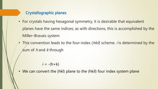
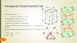
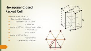
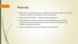
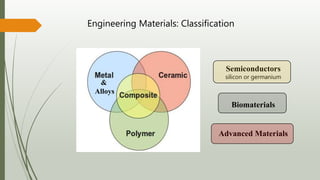
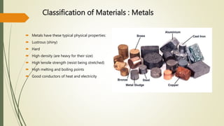
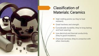
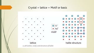
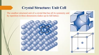
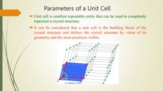
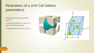
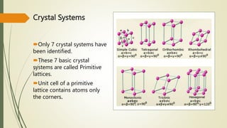
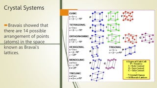
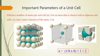
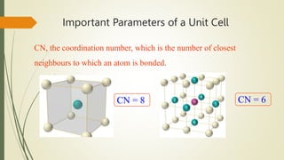
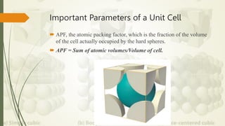
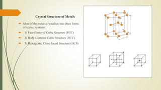
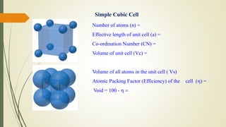
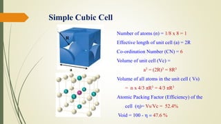
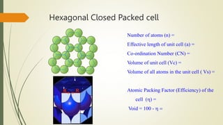
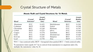
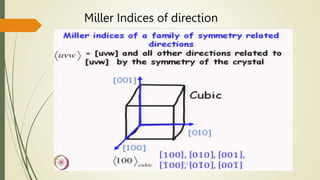
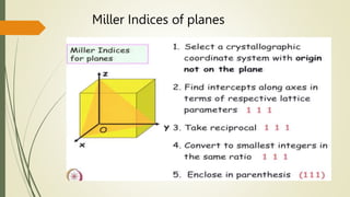
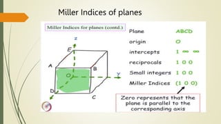
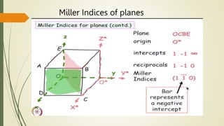
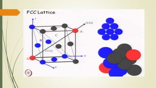
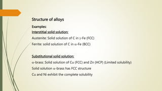
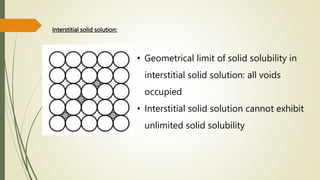
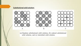
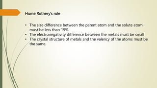
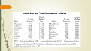
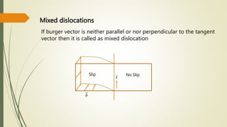
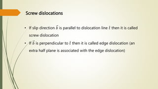
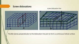
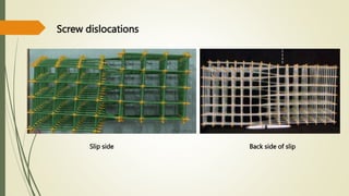
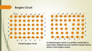
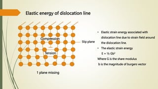
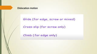
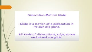
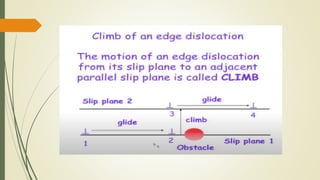
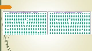
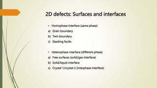
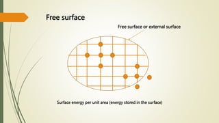
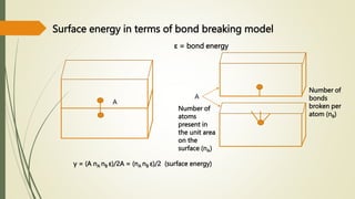
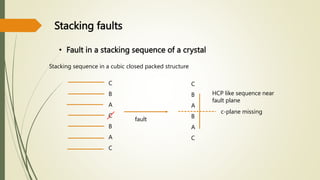
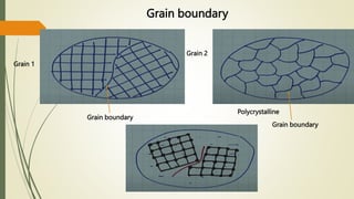
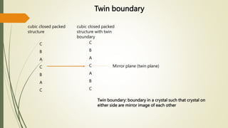
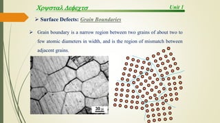
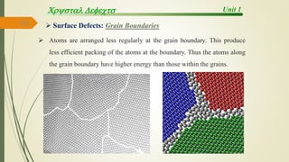
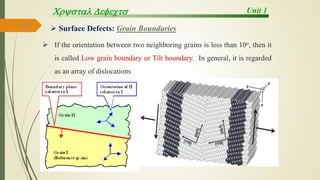
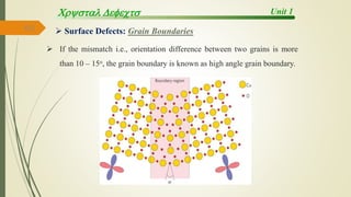
The document discusses materials science, focusing on the classification, properties, and structures of materials like metals, ceramics, and polymers. It details crystal geometry, unit cells, and different crystal systems including FCC, BCC, and HCP, along with the properties of alloys and defects in crystals. Additionally, it distinguishes between crystalline and non-crystalline materials, emphasizing the importance of crystalline structures in technology.

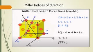
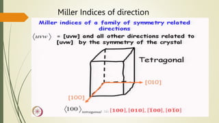
![Miller Indices of direction
Put in square brackets [1 0 0]](https://image.slidesharecdn.com/materialsscience-copy-240626111231-488ba925/85/Materials-Science-notes-ppt-for-1st-year-mechanical-engineering-pptx-28-320.jpg)
![Hexagonal Crystals
• The three and axes are all contained within a single plane (called the basal
plane) and are at 120 degree angles to one another.
• The z axis is perpendicular to this basal plane.
• Directional indices, will be denoted by four indices, as [uvtw];
Conversion from the three-index system to the four-index system](https://image.slidesharecdn.com/materialsscience-copy-240626111231-488ba925/85/Materials-Science-notes-ppt-for-1st-year-mechanical-engineering-pptx-108-320.jpg)