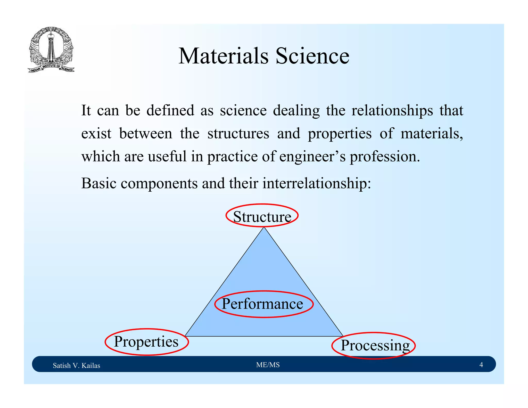
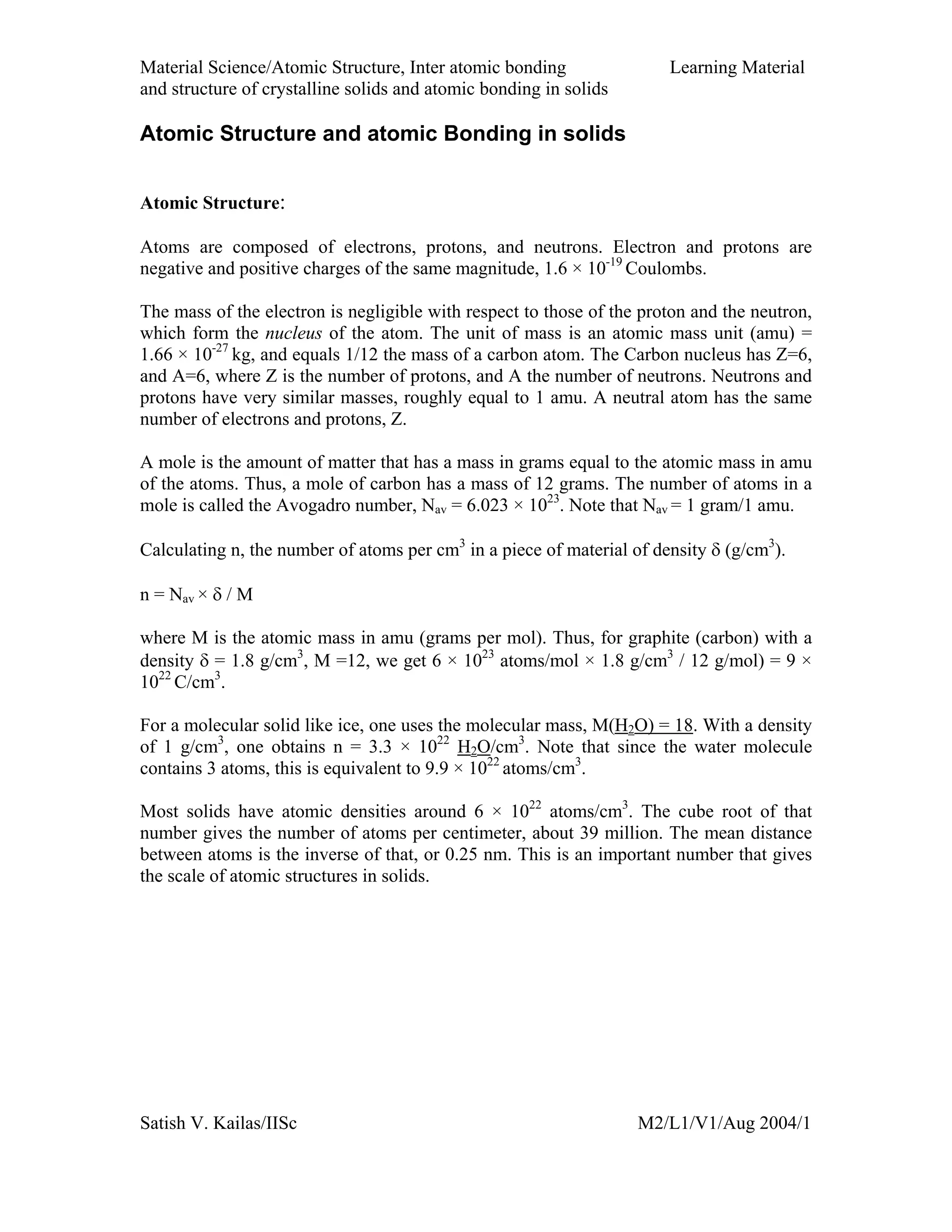
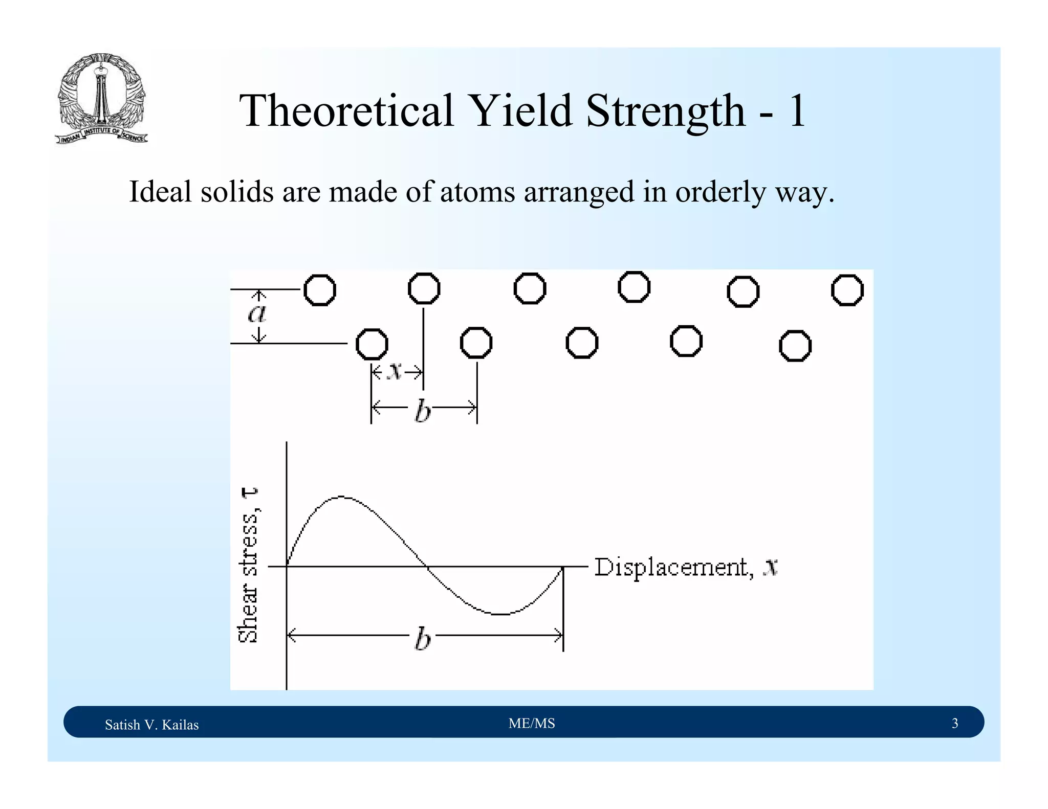
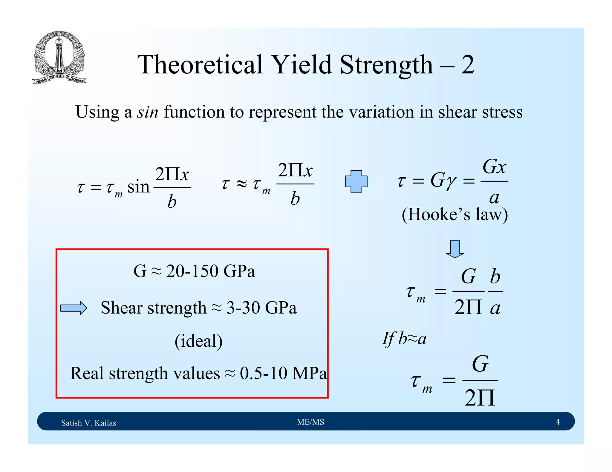
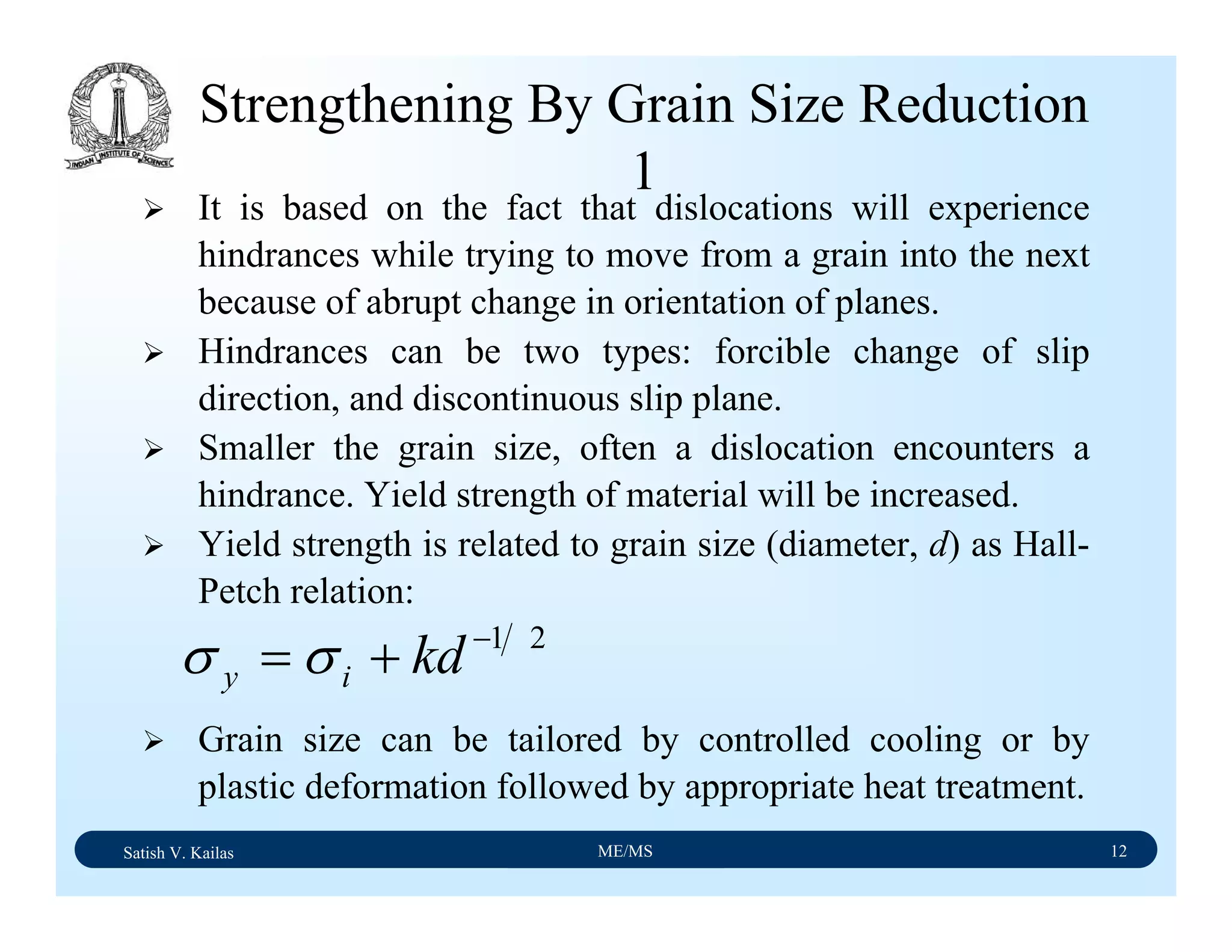
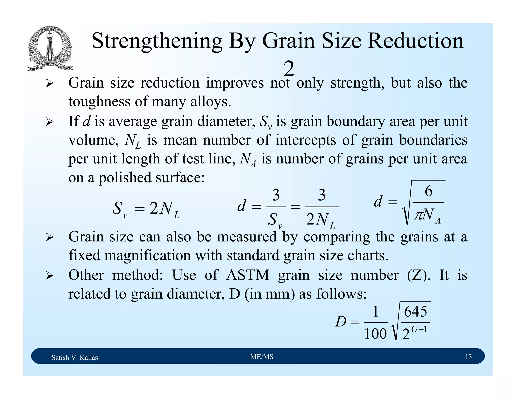
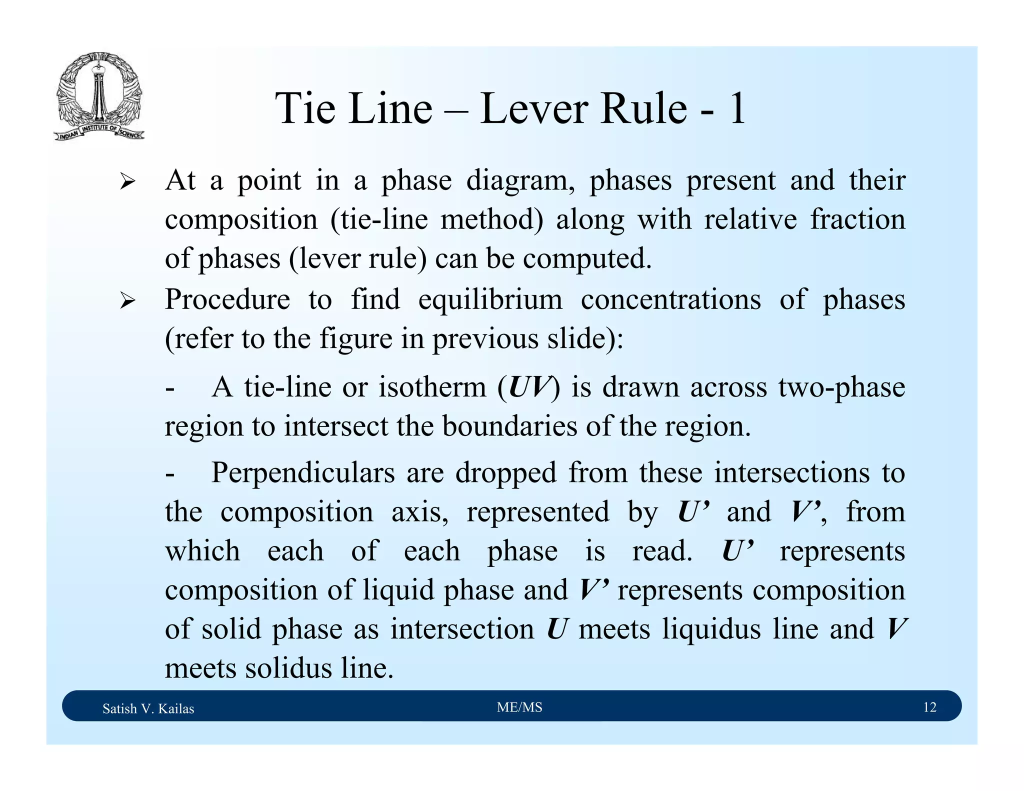
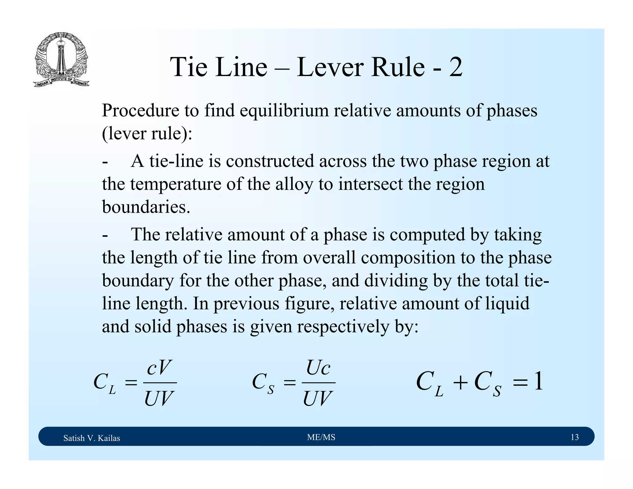
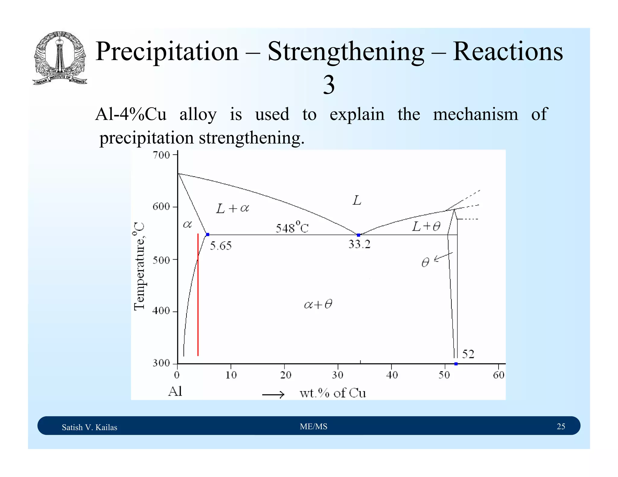
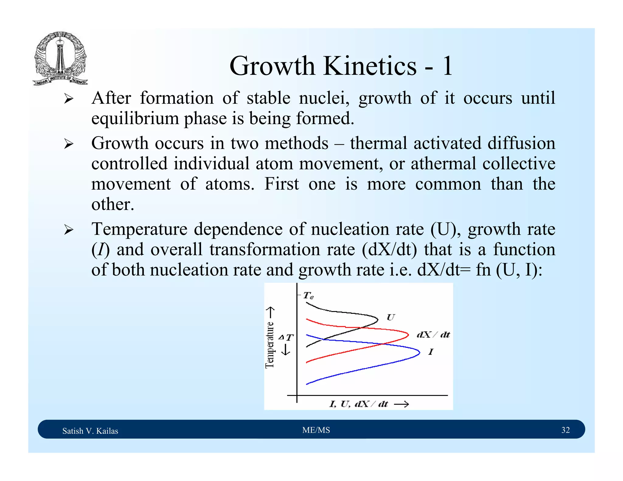
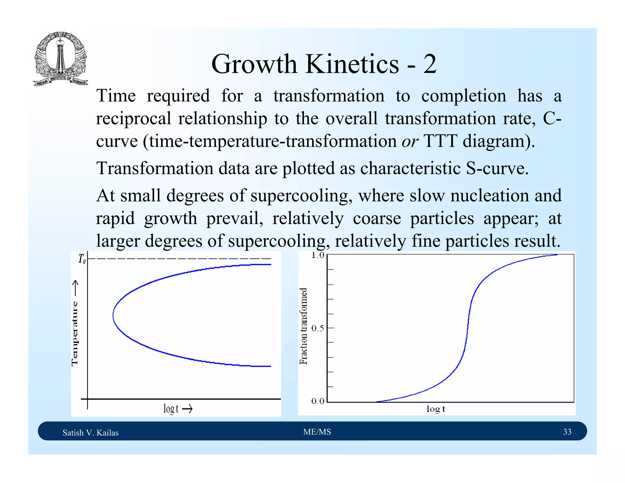
The document outlines the syllabus for a Material Science course with the following aims:
1) Provide an understanding of the mechanics, physical and chemical properties of materials including metals, ceramics, polymers and composites.
2) Cover 18 modules on topics ranging from atomic structure and bonding to mechanical properties, phase diagrams, applications and processing of different materials.
3) Total of 60 lecture hours to cover the various modules and learning units within each module.

![Satish V. Kailas ME/MS 19
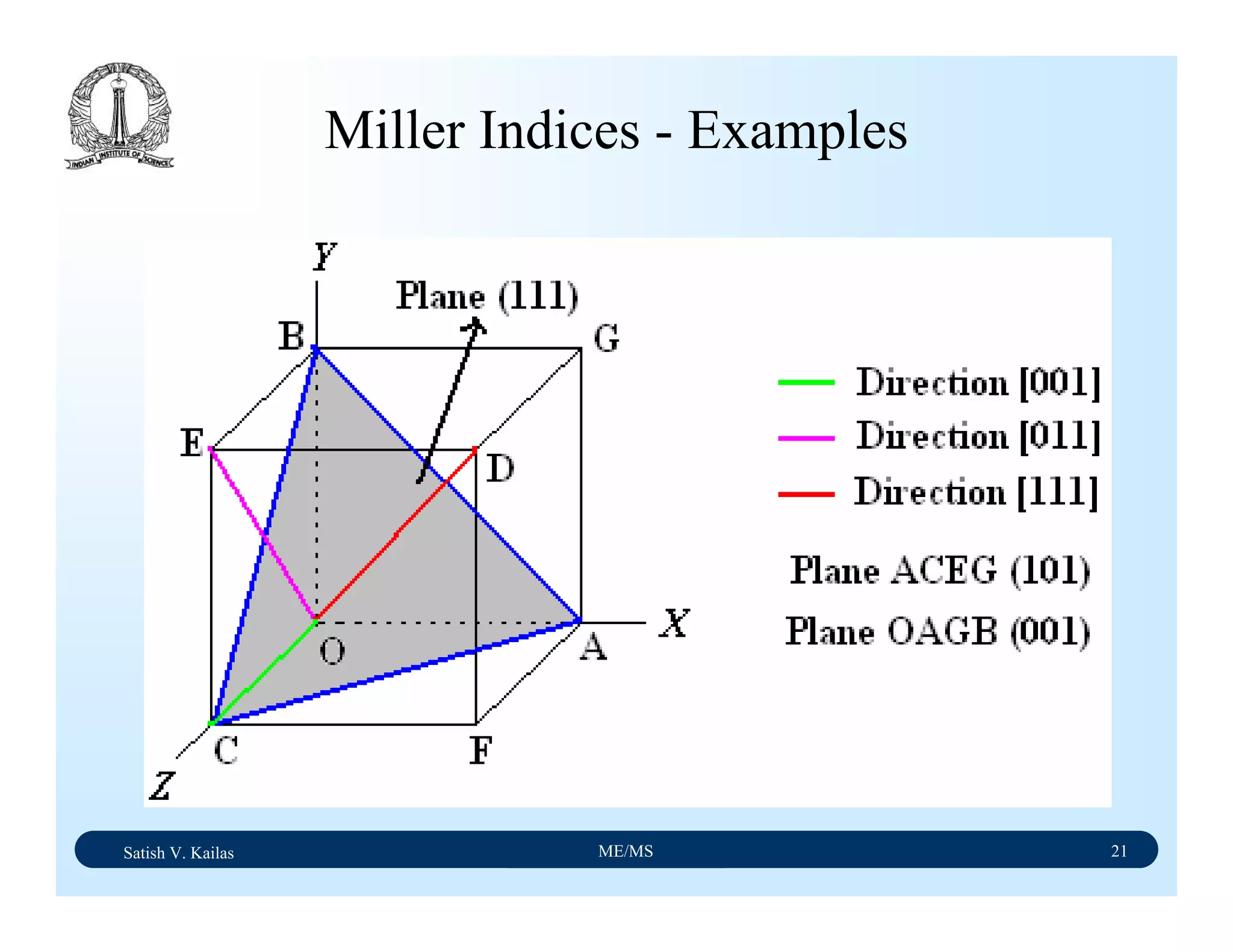
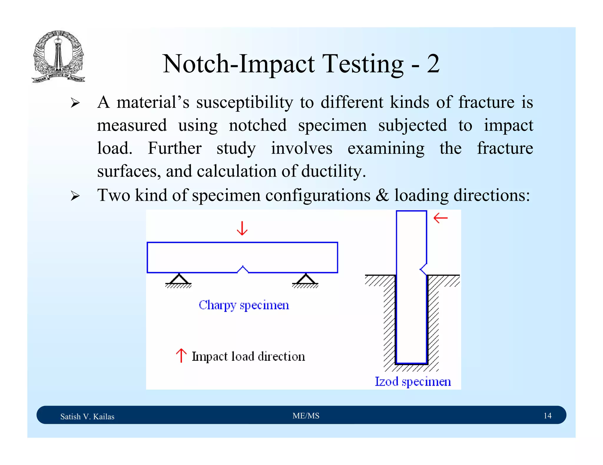
Miller Indices - Direction
A vector of convenient length is placed parallel to the
required direction
The length of the vector projection on each of three axes are
measured in terms of unit cell dimensions
These three numbers are made to smallest integer values,
known as indices, by multiplying or dividing by a common
factor
The three indices are enclosed in square brackets, [uvw].
A family of directions is represented by <uvw>](https://image.slidesharecdn.com/materialscience-160106071247/75/Material-science-notes-58-2048.jpg)
![Satish V. Kailas ME/MS 23
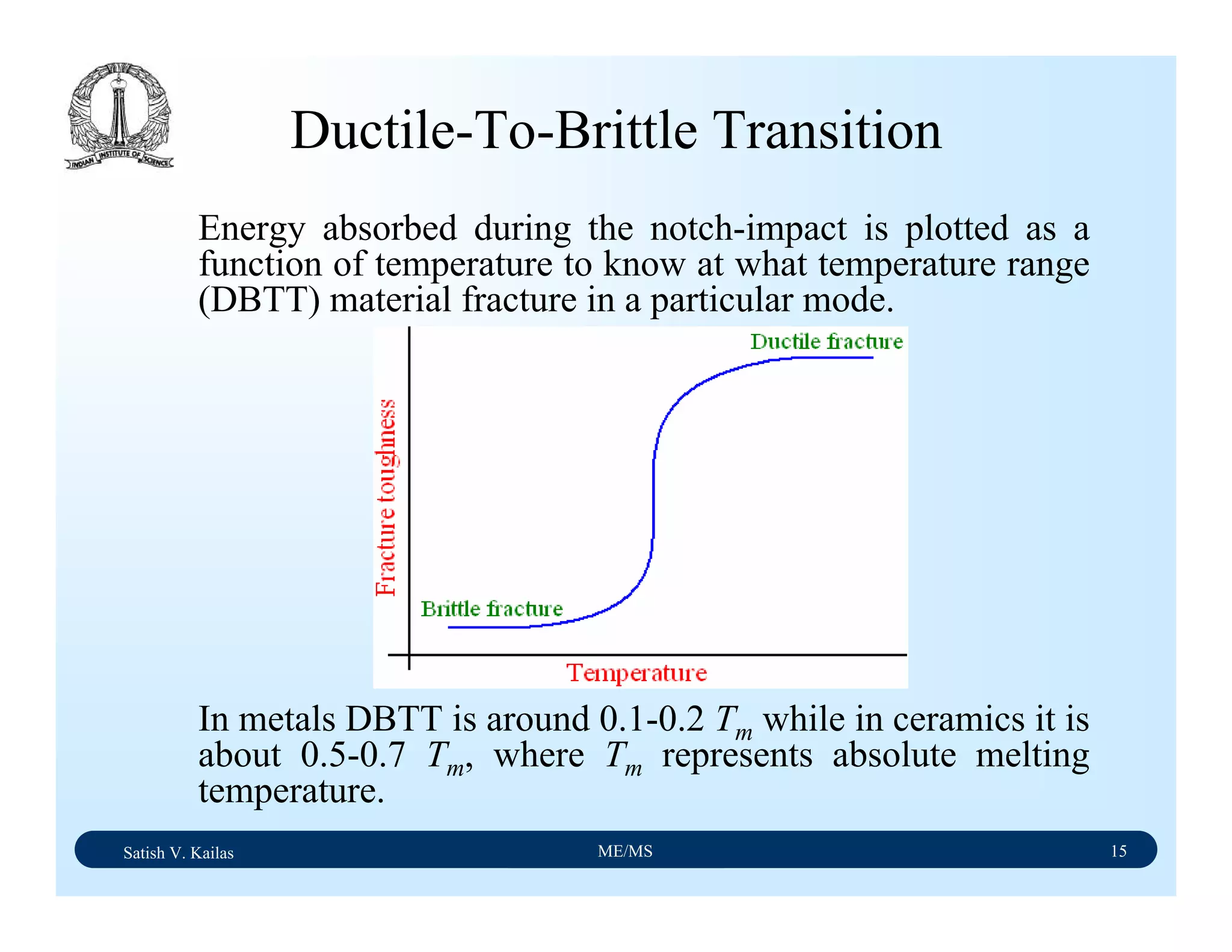
Useful Conventions For Cubic Crystals
[uvw] is normal to (hkl) if u = h, v = k, and w = l. E.g.: (111)
┴ [111]
[uvw] is parallel to (hkl) if hu + kv + lw = 0
Two planes (h1k1l1) and (h2k2l2) are normal if h1h2 + k1k2
+ l1l2=0
Two directions (u1v1w1) and (u2v2w2) are normal if u1u2 +
v1v2 + w1w2=0
Inter-planar distance between family of planes {hkl} is given
by:
Angle between two planes is given by:
222
}{
lkh
a
d hkl
++
=
2
2
2
2
2
2
2
1
2
1
2
1
212121
cos
lkhlkh
llkkhh
++++
++
=θ](https://image.slidesharecdn.com/materialscience-160106071247/75/Material-science-notes-62-2048.jpg)
![Satish V. Kailas ME/MS 24
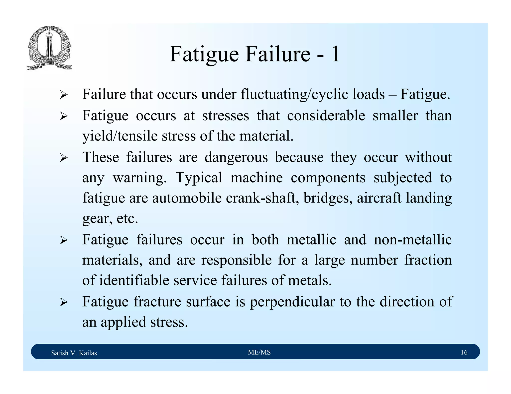
Miller-Bravis Indices
Miller indices can describe all possible planes/directions in
any crystal.
However, Miller-Bravis indices are used in hexagonal
systems as they can reveal hexagonal symmetry more clearly
Indices are based on four axes – three are coplanar on basal
plane at 120˚ apart, fourth axis is perpendicular to basal
plane
Both for planes/directions, extra index is given by
t = -(u+v), i = -(h+k)
where plane is represented as [uvtw], and a direction is
represented by (hkil)
E.g.: Basal plane – (0001), Prismatic plane – (10ֿ10)](https://image.slidesharecdn.com/materialscience-160106071247/75/Material-science-notes-63-2048.jpg)


![Satish V. Kailas ME/MS 18
Yielding Under Multi-Axial Stress
With on-set of necking, uni-axial stress condition turns
into tri-axial stress as geometry changes tales place. Thus
flow curve need to be corrected from a point
corresponding to tensile strength. Correction has been
proposed by Bridgman.
[ ])2/1ln()/21(
)(
RaaR
avgx
++
=
σ
σ
where
(σx)avg measured stress in the axial direction,
a – smallest radius in the neck region,
R – radius of the curvature of neck](https://image.slidesharecdn.com/materialscience-160106071247/75/Material-science-notes-122-2048.jpg)
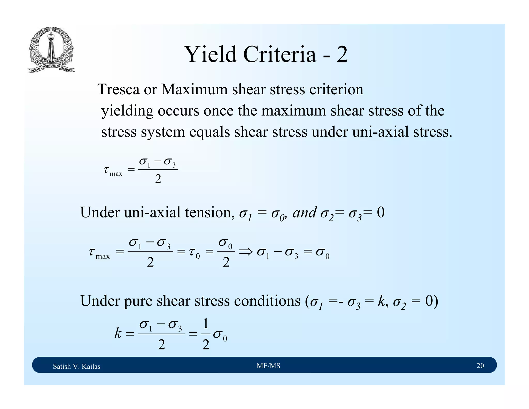
![Satish V. Kailas ME/MS 19
Yield Criteria - 1
Von Mises or Distortion energy criterion:
yielding occurs once second invariant of stress deviator
(J2) reaches a critical value. In other terms, yield starts
once the distortion energy reaches a critical value.
2
2 kJ = [ ]2
13
2
32
2
212 )()()(
6
1
σσσσσσ −+−+−=J
Under uni-axial tension, σ1 = σ0, and σ2= σ3= 0
[ ] 2
1
2
13
2
32
2
210
0
22
0
2
0
)()()(
2
1
3)(
6
1
σσσσσσσ
σσσ
−+−+−=⇒
=⇒=+ kk
00 577.0
3
1
σσ ==k where k – yield stress under shear](https://image.slidesharecdn.com/materialscience-160106071247/75/Material-science-notes-123-2048.jpg)

Zn, Cd, Mg, TiHCP
[111](112)α-Fe, TaBCC
[112](111)Ag, Au, CuFCC
Twin
direction
Twin planeExampleCrystal](https://image.slidesharecdn.com/materialscience-160106071247/75/Material-science-notes-159-2048.jpg)

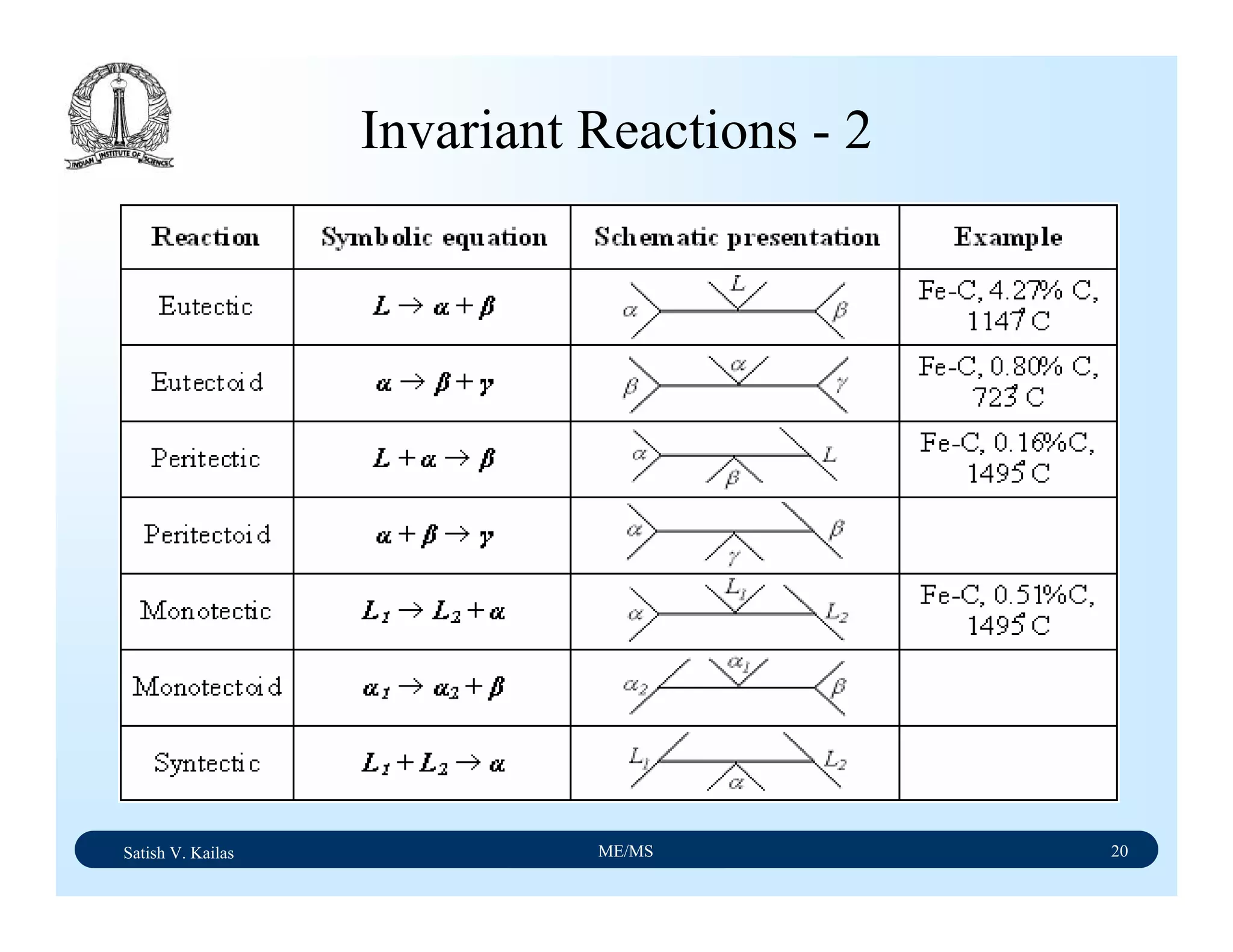
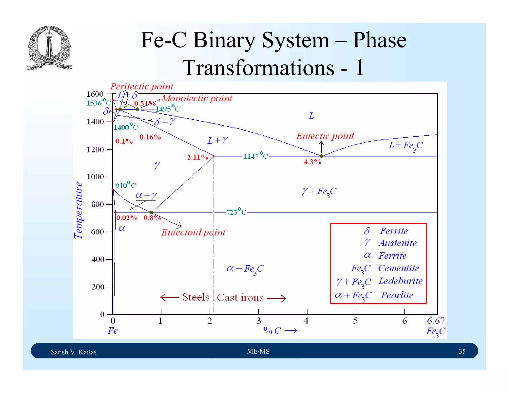
![Satish V. Kailas ME/MS 36
Fe-C Binary System – Phase
Transformations - 2
Fe-Fe3C phase diagram is characterized by five individual
phases,: α–ferrite (BCC) Fe-C solid solution, γ-austenite
(FCC) Fe-C solid solution, δ-ferrite (BCC) Fe-C solid
solution, Fe3C (iron carbide) or cementite - an inter-metallic
compound and liquid Fe-C solution and four invariant
reactions:
- peritectic reaction at 1495 ْC and 0.16%C, δ-ferrite + L
↔ γ-iron (austenite)
- monotectic reaction 1495 ْC and 0.51%C, L ↔ L + γ-iron
(austenite)
- eutectic reaction at 1147 ْC and 4.3 %C, L ↔ γ-iron +
Fe3C (cementite) [ledeburite]
- eutectoid reaction at 723 ْC and 0.8%C, γ-iron ↔ α–
ferrite + Fe3C (cementite) [pearlite]](https://image.slidesharecdn.com/materialscience-160106071247/75/Material-science-notes-223-2048.jpg)
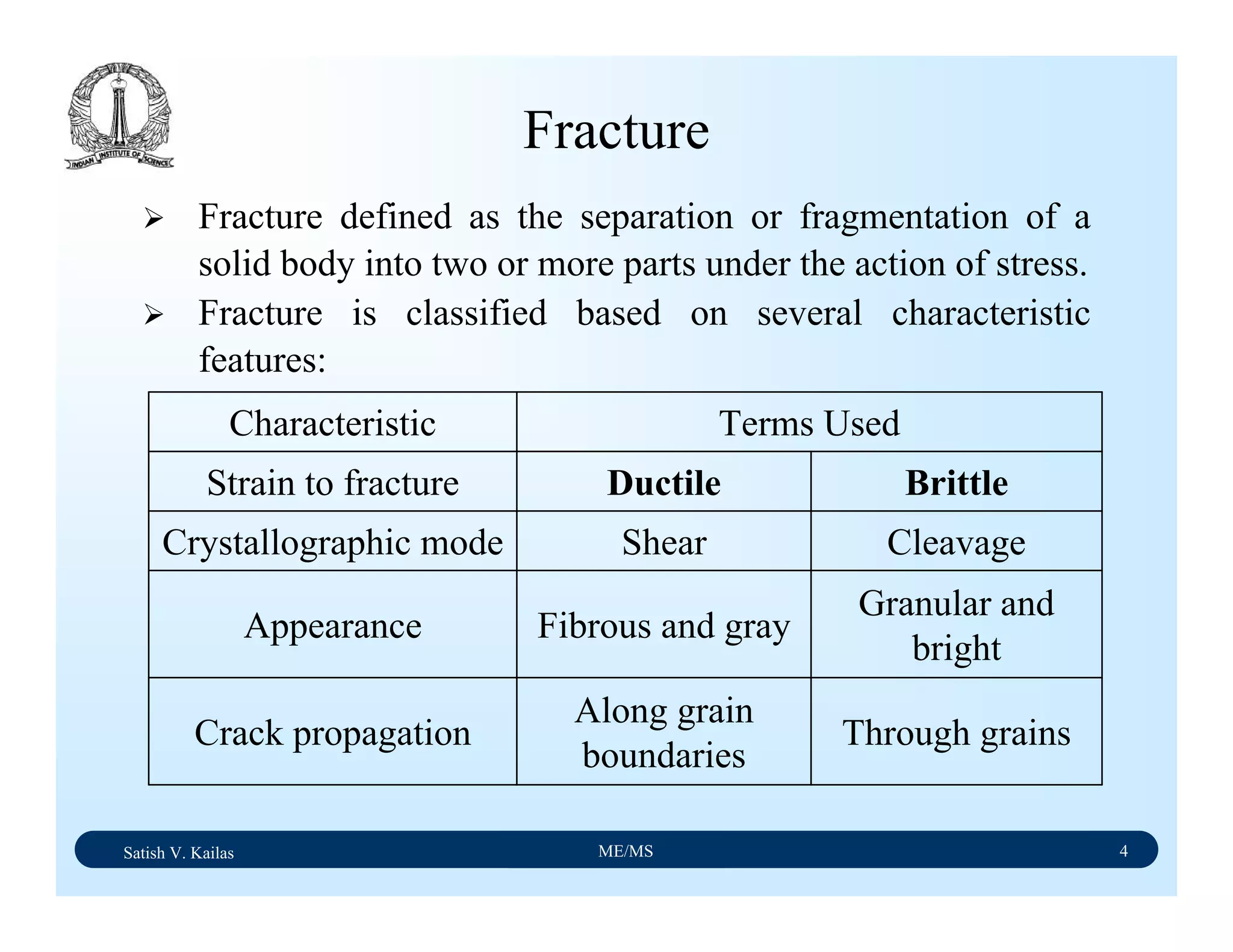
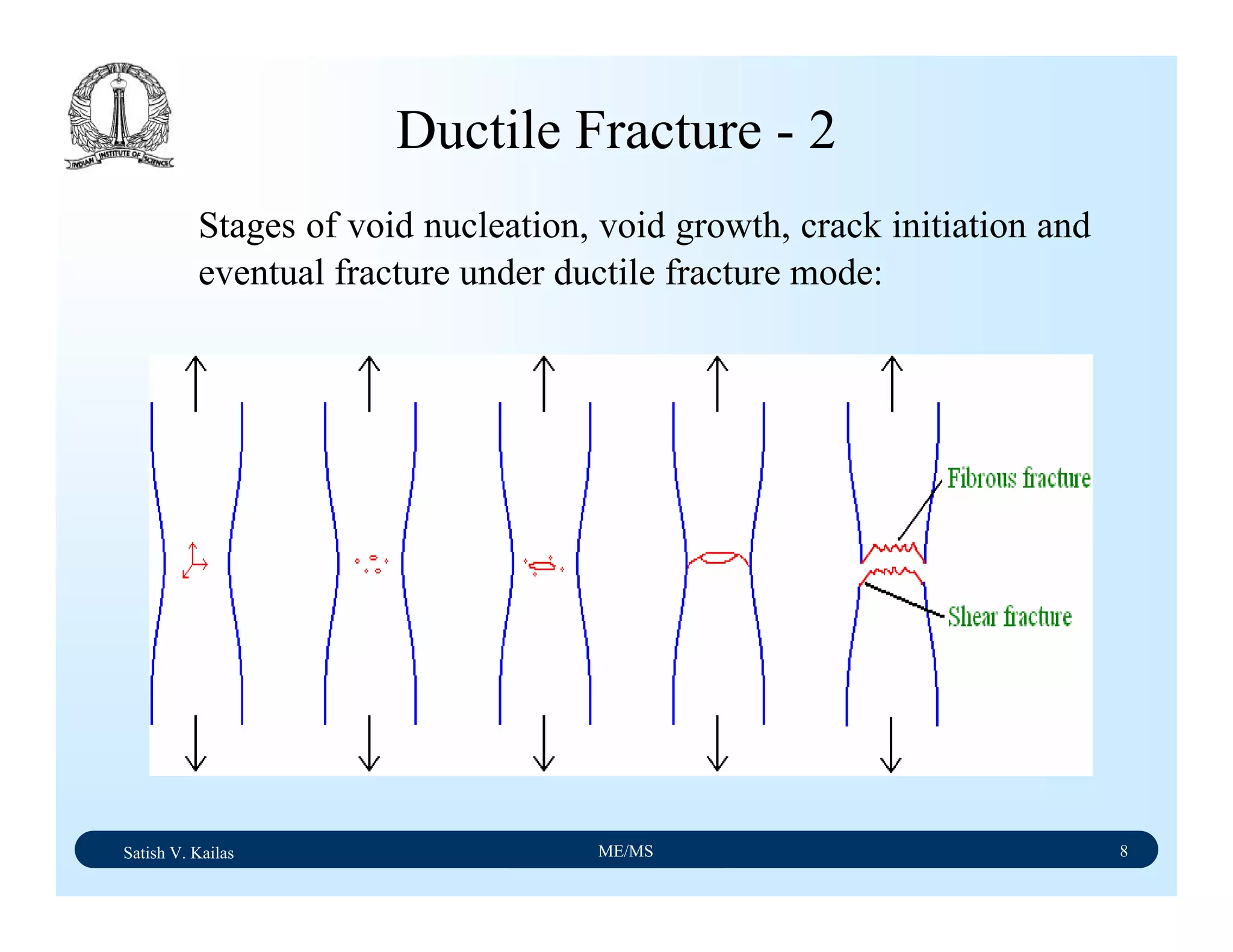
![Satish V. Kailas ME/MS 7
Ductile Fracture - 1
Ductile fracture in tension occurs after appreciable plastic
deformation.
It is usually preceded by necking.
It exhibits three stages - (1) formation of cavities (2)
growth of cavities (3) final failure involving rapid crack
propagation at about 45ْto the tensile axis.
Fractography of ductile fracture reveals numerous spherical
dimples separated by thin walls on the fractured surface.
McClintock’s strain to ductile fracture, εf,
[ ])32()()1(sinh
)2ln()1( 00
σσσ
ε
ba
f
n
bln
+−
−
=](https://image.slidesharecdn.com/materialscience-160106071247/75/Material-science-notes-242-2048.jpg)
![Material Science/Applications and Processing of Ceramics Lecture Notes
Satish Kailash Vasu/IISc, Bangalore M10/L1/V1/feb2005/2
compounds, including sulfur and carbon. The powder and petrurgic methods were
explored, and gave us products with different phases and microstructures. For the
sintering experiments, we mixed calcined ash powder with various amounts (10-50wt%)
of borosilicate (Pyrex) glass. The powder mixtures were uniaxial cold pressed to a
cylindrical shape and sintered in air at temperatures in the range of 1,000-1,500°C for
periods of up to 15 hours. Using the petrurgic method, coal ash was mixed with soda-
lime glass powder. The mixture was melted at 1,500°C and cooled to room temperature
at rates of between 1-10°C per minute.
Glass-Ceramic Composites
Work to date has largely concentrated on composites with a matrix of the slag-based
Silceram glass-ceramic (a glass-ceramic for floor and wall tiles and wear components).
We have investigated both particulate- (SiC and TiC) and fibre-reinforcement (SiC).
Properties measured include the fundamental mechanical properties but also more
complex properties such as thermal shock resistance and erosion resistance. As
mentioned previously, the thermal shock resistance of glass-ceramics is superior to the
parent glasses, and the shock resistance is further improved by particulate reinforcement.
For example, monolithic Silceram has a thermal shock critical temperature of 180°C,
whereas a 20wt%SiC composite has a value of 270°C. Erosion resistance may also be
improved by particulate reinforcement, e.g., for TiC reinforced Silceram - the larger the
reinforcement particle size and the greater the volume fraction, the lower the erosion rate.
Results indicate a way for transforming vitrified silicate residues into useful products
with broad application potential. The glass-ceramics obtained are candidate materials for
applications in floors of industrial buildings and in construction, and for outside and
inside facing walls. We are currently addressing issues associated with the effect of
environmental influences on the chemical durability and toxic potential of the materials,
which may be compromised by the presence of heavy metals incorporated in the glass or
crystalline phases. Public acceptance of the use and exploitation of glass-ceramic-based
materials in such applications will strongly depend on a satisfactory consideration of
these issues.
2) Refractories -Refractories are materials needed for handling high temperature liquids,
gases and solids, e.g., for industrial processing. Applications include solar furnaces,
casting molds for molten materials, heat exchangers, and aerobraking heat shields.
Industrial refractory needs can be satisfied by sintered calcia (CaO), silica (SiO2),
magnesia (MgO), alumina (Al2O3) and titania (TiO2), with the desired porosity. Of
course, these stable materials are commonly used on Earth for the same purposes, due to
their great resistance to heat, oxidation (they are already fully oxidized), corrosion and
abrasion. Minerals such as olivine [(MgFe)2SiO4] and anorthite (CaAl2Si2O8) are also
useful for making refractory bricks and ceramics. Some refractories and their ceramics
have low expansion due to heat and are attractive for space environments where a wide
range of temperatures are experienced.](https://image.slidesharecdn.com/materialscience-160106071247/75/Material-science-notes-293-2048.jpg)
![Material Science/Applications and Processing of Ceramics Lecture Notes
Satish Kailash Vasu/IISc, Bangalore M10/L1/V1/feb2005/8
processing has enabled the development of direct-fabrication processes. Furthermore, we
are developing phenomenological sintering models to enhance both ceramic component
design and manufacturing capability.
Ceramic Synthesis and Processing Research Briefs:
Constrained Sintering of Multi-Material Systems
Development of A Predictive Model for Ceramic Powder Compaction
ESP (Engineered Stress Profile) Glass - Unique Opportunities for Performance
and Reliability
Molecular Dynamics Simulations of Reactive Wetting in Ceramic-Metal Systems
PZT 95/5 Material Development for Neuron Generator Applications
Precursor's Structure Effects on Thin-Film Densification of TiO2
Relationship between Interfacial Interactions and Fracture Stress for Adhesive
Joints in Mode II Loading
Robocasting : Layered Manufacturing by Slurry Extrusion
Synthesis and Processing of Composites by Reactive Metal Penetration
10.3 Electrical conduction in ionic ceramics and in polymers:
This requires creation of electron [e'] and hole [h⋅] pairs in ionic solid according to the
symbolic chemical reaction, which describes creation of carriers due to thermal activation
(this process results in intrinsic conductivity):
nil ⇔ e' + h⋅
K = [e'] + [h⋅ ] = n . p = exp (- ∆G0
/RT) = exp (∆S0
/R) exp (-Eg /RT)
Accordingly, a supply of "band gap" energy Eg is necessary, hence the strong
dependence of conductivity on temperature. The equilibrium constant of the above
reaction can be approximately expressed as: n.p ≈ 1019exp(Eg/kT), or, the carrier
concentration (assuming the same concentration of holes p and electrons e), c ≈
109.5exp(Eg/2kT).](https://image.slidesharecdn.com/materialscience-160106071247/75/Material-science-notes-299-2048.jpg)
![Material Science/Applications and Processing of Ceramics Lecture Notes
Satish Kailash Vasu/IISc, Bangalore M10/L1/V1/feb2005/9
The magnitude of the band gap Eg determines ability of a material to conduct. For Eg > 6
eV, materials are considered as insulators . This wide energy gap is typical for the
ionic oxides of metals having a single stable oxidation state: groups IA, IIA, IIIA. The
electrical resistivity of most stable insulators correlates with the ionic character of their
bond: the larger difference of electronegativity, the larger % of ionic bond, and the larger
energy gap Eg.
The band gap magnitude correlates also with the ionic bond energy, i.e. the most stable
ionic ceramic are also the best insulators. For example, the bond energy of alumina is
~6eV/equivalent (1/3 Al2O3) and Eg = ~7eV; the bond energy of one equivalent of
cadmium oxide (CdO) is ~4 eV/equivalent and Eg = ~2eV.
The oxides of metals able to have multiple oxidation states (such as transition elements,
with partially filled "d" orbitals) have narrower band gaps of the order of 2-5eV, resulting
in intrinsic semiconducting properties. The presence of point defects in ionic solids
(such as solutes, vacancies, interstistials) can dramatically decrease the energy required
for the creation of electron/hole pairs.
This is because these defects are typically located “within” the energy gap, either close to
the valence band (acceptors) or conduction band (donors). An example is KCl
containing VK', VCl
•, CaK
• , or MgO containing VMg'', VO
•,VMg', VC
0, AlMg
•.
The point defects are the key feature of extrinsic semiconductors, the basic components
of modern electronics.
Mixed and Ionic Ceramic Conductors
The variety of point defects present in ceramics gives frequently a mixed ionic and
electronic type of electrical conduction. To some extent, every ionic crystal is a mixed
conductor, but the share of electronic conductivity, expressed through the charge
transference number for electrons, can be negligible. If Ohm’s law is expressed in
terms of current density J [A/m2
], material conductivity σ [A/Vm] and electric field Ee,
[V/m] following relationship results:
J = - σ.Ee](https://image.slidesharecdn.com/materialscience-160106071247/75/Material-science-notes-300-2048.jpg)
![Material Science/Applications and Processing of Ceramics Lecture Notes
Satish Kailash Vasu/IISc, Bangalore M10/L1/V1/feb2005/10
where, for mixed a conductor, σ = Σσi, the sum of conductvities due to the various
charge-carrying species, i.e. ions, holes and electrons. The transference number ti of a
given species is then defined as: tj = σj/Σσi
For ionic conductors, the aim is to maximize the charge transference due to the
movement of ions and minimize the transference due to electrons and holes movement.
That is, tion ≈ 1 , te,h ≈ 0 . This is principle behind the operation of solid
electrolytes. The sub-class of solid electrolytes useful for solid-state electrochemical
devices (batteries, sensors) can be defined as "fast ionic conductors" as long as:
1. The activation energy Ed for diffusion is LOW, less than ~0.1 eV/atom, or
2.5 kcal/mole, or 10 kJ/mole, or ~10% of the energy needed to form a point defect in a
close packed ionic solid.
2. The corresponding D0 value (diffusion coefficient D = D0exp[-Ed/kT], so
D = D0 at T = ∞) is HIGH (D0 >10-4 cm2/s) and therefore the corresponding σ0 value
(ionic conductivity σ=σ0exp[-E/kT]) is HIGH, σ0 > 0.1 1/Ω.cm.
If the above conditions are fulfilled, the diffusivity at room temperature will be D > 10-6
cm2/s, and room temperature ionic conductivity will be σ > 0.01 1/Ωcm, or resistivity ρ
= 100 Ωcm . This magnitude of conductivity allows the use of solid state ionic
conductors in devices like batteries, sensors and fuel cells.
The resistivity of ionic conductor is the primary factor that determines internal resistance
of the cell, and thus maximum current that can be drawn from the cell. As resistance R
= ρ L/A (L being electrolyte thickness, typically 0.1-1 cm, and A area, typically 10-1000
cm2
), then the internal resistance of such battery is typically 1 Ω .](https://image.slidesharecdn.com/materialscience-160106071247/75/Material-science-notes-301-2048.jpg)


![[S.L._Kakani]_Material_Science_(New_Age_Pub.,_2006(BookSee.org).pdf](https://cdn.slidesharecdn.com/ss_thumbnails/s-230301071329-4f25d7e9-thumbnail.jpg?width=640&height=640&fit=bounds)


