Downloaded 460 times


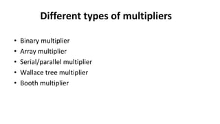
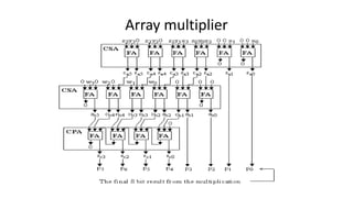

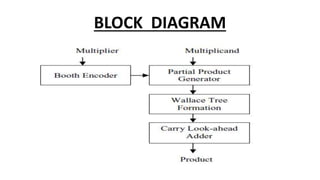

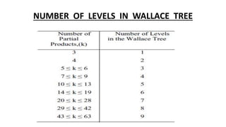

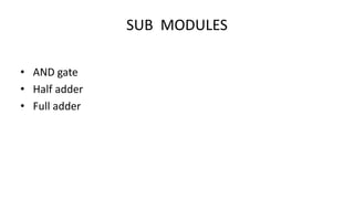


This document describes the design of a Wallace tree multiplier using Verilog. It discusses different types of multipliers such as array, serial/parallel, and Booth multipliers. It provides details on the Wallace tree multiplier design including its block diagram, partitioning of partial products, number of levels, submodules like AND gates and full adders, and comparison of its power consumption and results. The dumping process in an FPGA kit is also covered along with the advantage of small delay and disadvantage of complex layout for the Wallace tree multiplier.