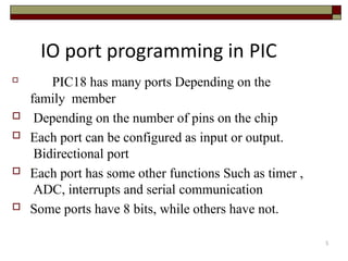
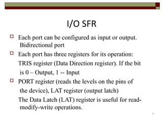
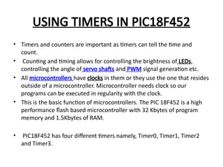
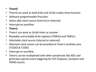
Department of Electronics & Telecommunication Engineering
_______________________________________________________________________________________________________________________
Unit-05
PIC Microcontroller Architecture
Lecture 1
Assist.Prof. C.K.Kalawade
(M.E.(Electronics &Telecommunication ))
MCU Support Devices




ToCON
2
3
4
{}
{}
{}
5
IO port programming in PIC

PIC18 has many ports Depending on the
family member
 Depending on the number of pins on the chip
 Each port can be configured as input or output.
Bidirectional port
 Each port has some other functions Such as timer ,
ADC, interrupts and serial communication
 Some ports have 8 bits, while others have not.
6
I/O SFR
 Each port can be configured as input or output.
Bidirectional port
 Each port has three registers for its operation:
TRIS register (Data Direction register). If the bit
is 0 – Output, 1 -- Input
 PORT register (reads the levels on the pins of
the device), LAT register (output latch)
The Data Latch (LAT) register is useful for read-
modify-write operations.
LED interfacing with PIC18fxxx
Programming steps:
1. Configure the TRISB register to make PortB as
output port.
2. Set all the bits of PORTB register High (1) to
glow all LEDs.
3. Provide some delay.
4. Set all the bits of PORTB register Low (0) to
turn off the LEDs.
5. Provide some delay.
6. Repeat the process from step 2.
#include<p18f4520.h>
void delay (unsigned int itime);
#pragma config OSC=HS
#pragma config PWRT=OFF
#pragma config WDT=OFF
#pragma config DEBUG=OFF, LVP=OFF
void main()
{
TRISB = 0; // PORTB AS OUTPUT PORT
while(1)
{
• PORTB = 0X00; // PORTB AS HIGH
• delay(100);
• PORTB = 0Xff; // PORTB AS LOW
• delay (100);
}
}
• void delay (unsigned int itime)
• {
• int i,j;
• for(i=0;i<=itime;i++)
• for(j=0;j<=1275;j++);
• }
• The ‘#pragma’ directive is the method
specified by the C standard for providing
additional information to the compiler,
beyond what is conveyed in the language
itself.
Department of Electronics & Telecommunication Engineering
_______________________________________________________________________________________________________________________
Unit-05
PIC Microcontroller Architecture
Lecture 2
Assist.Prof. C.K.Kalawade
(M.E.(Electronics &Telecommunication ))
LCD Display
LCD interfacing with PIC 18fxxx in 8bit mode
Steps in programming
• 1) initialize port pins connected to lcd as o/p
• 2)initialize LCd display
• 3)send data to lcd for diplaying on it
Lcd initializations
• lcdcmd(0x38); /*Double Line Display Command
• lcdcmd(0x0C); /*display on cursor off*/
• lcdcmd(0x01); /*Clear Display Command
• lcdcmd(0x06); /*Auto Increment Location Address Command
• lcdcmd(0x81); /*first line first position
Command loop
void lcdcmd (unsigned char value)
{
ldata=value;
rs=0;
rw=0;
en=1;
msdelay(1);
en=0;
}
Lcd data loop
void lcddata (unsigned char value)
{
ldata=value;
rs=1;
rw=0;
en=1;
msdelay(1);
en=0;
}
Department of Electronics & Telecommunication Engineering
_______________________________________________________________________________________________________________________
Unit-05
PIC Microcontroller Architecture
Lecture 3
Assist.Prof. C.K.Kalawade
(M.E.(Electronics &Telecommunication ))
Pic 187f458 interfacing with LCD in 4-bit Mode
• In 4-bit mode, data/command is sent in a 4-bit
(nibble) format.
• To do this 1st send Higher 4-bit and then send
lower 4-bit of data/command.
Why 4bit mode
• Only 4 data (D4 - D7) pins of 16x2 of LCD are
connected to the microcontroller and other
control pins i.e. RS (Register select), RW
(Read/write), E (Enable) are connected to
other GPIO Pins of the controller.
• Therefore, due to such connections, we can
save four GPIO pins which can be used for
another application.
void lcdcmd (unsigned char value)
{
unsigned char temp;
temp=value;
value=value & 0xf0;
ldata=value;
rs=0;
rw=0;
en=1;
msdelay(1);
en=0;
value=temp;
value=value << 4;
ldata=value;
en=1;
msdelay(1);
en=0;
}
Department of Electronics & Telecommunication Engineering
_______________________________________________________________________________________________________________________
Unit-05
PIC Microcontroller Architecture
Lecture 4
Assist.Prof. C.K.Kalawade
(M.E.(Electronics &Telecommunication ))
USING TIMERS IN PIC18F452
• Timers and counters are important as timers can tell the time and
count.
• Counting and timing allows for controlling the brightness of LEDs,
controlling the angle of servo shafts and PWM signal generation etc.
• All microcontrollers have clocks in them or they use the one that resides
outside of a microcontroller. Microcontroller needs clock so our
programs can be executed in regularity with the clock.
• This is the basic function of microcontrollers. The PIC 18F452 is a high
performance flash based microcontroller with 32 Kbytes of program
memory and 1.5Kbytes of RAM.
• PIC18F452 has four different timers namely, Timer0, Timer1, Timer2
and Timer3.
• Timer0:
• Timer0 can work as both 8-bit and 16-bit modes timer/counter
• Software programmable Prescaler
• Select able clock source (internal or external)
• Interrupt on overflow
• Timer1:
• Timer1 can work as 16-bit timer or counter
• Readable and writable 8-bit registers (TMR1H and TMR1L)
• Selectable clock source (internal or external)
• Alternate clock source can be provided at Timer1 oscillator pins
(T1OSO & T1OSI)
• Interrupt on overflow
• Timer1 can be multiplexed with other peripherals like ADC and
generates special event triggering for CCP (Capture, Compare and
PWM) events.
• Timer2:
• 8-bit Timer and Period registers (TMR2 and PR2, respectively)
• Software programmable prescaler (1:1, 1:4 and 1:16)
• Software programmable postscaler (1:1 – 1:16)
• Interrupt on TMR2 to PR2 match
• Timer3:
• Timer3 can work as 16-bit timer or counter
• Readable and writable 8-bit registers (TMR3H and TMR3L)
• Selectable clock source (internal or external)
• Alternate clock source can be provided at Timer1 oscillator pins
(T1OSO & T1OSI)
• Interrupt on overflow
• Timer3 can be multiplexed with other peripherals like ADC and
generates special event triggering for CCP (Capture, Compare and
PWM) events.
Timer0 Control Register:
• TMR0ON: Timer0 on/off bit
• This bit is set to high to enable the Timer0.
• 1 = Enable the Timer0
0 = to stop Timer0
• TMR0IE: Timer0 Interrupt Enable
• This bit is used to enable/disable the Timer0 overflow interrupt.
• 1 = TMR0 Interrupt enabled
0 = TMR0 Interrupt disabled
• TMR0 (Timer0 Register):
• This register is divided into registers
• TMR0H
• TMR0L
• #include <P18f4520.h>
• #pragma config OSC=HS
• #pragma config PWRT=OFF
• #pragma config WDT=OFF
• #pragma config DEBUG=OFF, LVP=OFF
• unsigned char data;
• void timer0(void);
• void main()
• {
• TRISB=0X00; // COnfigurePortB as output Port.
• PORTB=0x00;
• ADCON1=0x0F;
• while(1)
• {
• PORTB=~PORTB;
• timer0();
• }
• }
• void timer0(void)
• {
• T0CON=0x01;
• TMR0H=0x00; //Placing hiogher byte in TMR0H
• TMR0L=0X00; // Placing Lower byte in TMR0L
• T0CONbits.TMR0ON=1; // Timer0 On
• while(INTCONbits.TMR0IF==0); //Wait until TMR0IF
• gets flagged
•
• T0CONbits.TMR0ON=0; // Timer0 Off
• INTCONbits.TMR0IF=0; // Clear Timer0 interrupt flag
• }

pic microcontroller unit 5 detailed .pptx

  • 1.
    Department of Electronics& Telecommunication Engineering _______________________________________________________________________________________________________________________ Unit-05 PIC Microcontroller Architecture Lecture 1 Assist.Prof. C.K.Kalawade (M.E.(Electronics &Telecommunication ))
  • 2.
  • 3.
  • 4.
  • 5.
    5 IO port programmingin PIC  PIC18 has many ports Depending on the family member  Depending on the number of pins on the chip  Each port can be configured as input or output. Bidirectional port  Each port has some other functions Such as timer , ADC, interrupts and serial communication  Some ports have 8 bits, while others have not.
  • 6.
    6 I/O SFR  Eachport can be configured as input or output. Bidirectional port  Each port has three registers for its operation: TRIS register (Data Direction register). If the bit is 0 – Output, 1 -- Input  PORT register (reads the levels on the pins of the device), LAT register (output latch) The Data Latch (LAT) register is useful for read- modify-write operations.
  • 7.
  • 8.
    Programming steps: 1. Configurethe TRISB register to make PortB as output port. 2. Set all the bits of PORTB register High (1) to glow all LEDs. 3. Provide some delay. 4. Set all the bits of PORTB register Low (0) to turn off the LEDs. 5. Provide some delay. 6. Repeat the process from step 2.
  • 10.
    #include<p18f4520.h> void delay (unsignedint itime); #pragma config OSC=HS #pragma config PWRT=OFF #pragma config WDT=OFF #pragma config DEBUG=OFF, LVP=OFF void main() { TRISB = 0; // PORTB AS OUTPUT PORT while(1) { • PORTB = 0X00; // PORTB AS HIGH • delay(100); • PORTB = 0Xff; // PORTB AS LOW • delay (100); } }
  • 11.
    • void delay(unsigned int itime) • { • int i,j; • for(i=0;i<=itime;i++) • for(j=0;j<=1275;j++); • }
  • 12.
    • The ‘#pragma’directive is the method specified by the C standard for providing additional information to the compiler, beyond what is conveyed in the language itself.
  • 13.
    Department of Electronics& Telecommunication Engineering _______________________________________________________________________________________________________________________ Unit-05 PIC Microcontroller Architecture Lecture 2 Assist.Prof. C.K.Kalawade (M.E.(Electronics &Telecommunication ))
  • 14.
  • 15.
    LCD interfacing withPIC 18fxxx in 8bit mode
  • 16.
    Steps in programming •1) initialize port pins connected to lcd as o/p • 2)initialize LCd display • 3)send data to lcd for diplaying on it
  • 17.
    Lcd initializations • lcdcmd(0x38);/*Double Line Display Command • lcdcmd(0x0C); /*display on cursor off*/ • lcdcmd(0x01); /*Clear Display Command • lcdcmd(0x06); /*Auto Increment Location Address Command • lcdcmd(0x81); /*first line first position
  • 18.
    Command loop void lcdcmd(unsigned char value) { ldata=value; rs=0; rw=0; en=1; msdelay(1); en=0; }
  • 19.
    Lcd data loop voidlcddata (unsigned char value) { ldata=value; rs=1; rw=0; en=1; msdelay(1); en=0; }
  • 20.
    Department of Electronics& Telecommunication Engineering _______________________________________________________________________________________________________________________ Unit-05 PIC Microcontroller Architecture Lecture 3 Assist.Prof. C.K.Kalawade (M.E.(Electronics &Telecommunication ))
  • 21.
    Pic 187f458 interfacingwith LCD in 4-bit Mode • In 4-bit mode, data/command is sent in a 4-bit (nibble) format. • To do this 1st send Higher 4-bit and then send lower 4-bit of data/command.
  • 22.
    Why 4bit mode •Only 4 data (D4 - D7) pins of 16x2 of LCD are connected to the microcontroller and other control pins i.e. RS (Register select), RW (Read/write), E (Enable) are connected to other GPIO Pins of the controller. • Therefore, due to such connections, we can save four GPIO pins which can be used for another application.
  • 24.
    void lcdcmd (unsignedchar value) { unsigned char temp; temp=value; value=value & 0xf0; ldata=value; rs=0; rw=0; en=1; msdelay(1); en=0; value=temp; value=value << 4; ldata=value; en=1; msdelay(1); en=0; }
  • 25.
    Department of Electronics& Telecommunication Engineering _______________________________________________________________________________________________________________________ Unit-05 PIC Microcontroller Architecture Lecture 4 Assist.Prof. C.K.Kalawade (M.E.(Electronics &Telecommunication ))
  • 26.
    USING TIMERS INPIC18F452 • Timers and counters are important as timers can tell the time and count. • Counting and timing allows for controlling the brightness of LEDs, controlling the angle of servo shafts and PWM signal generation etc. • All microcontrollers have clocks in them or they use the one that resides outside of a microcontroller. Microcontroller needs clock so our programs can be executed in regularity with the clock. • This is the basic function of microcontrollers. The PIC 18F452 is a high performance flash based microcontroller with 32 Kbytes of program memory and 1.5Kbytes of RAM. • PIC18F452 has four different timers namely, Timer0, Timer1, Timer2 and Timer3.
  • 27.
    • Timer0: • Timer0can work as both 8-bit and 16-bit modes timer/counter • Software programmable Prescaler • Select able clock source (internal or external) • Interrupt on overflow • Timer1: • Timer1 can work as 16-bit timer or counter • Readable and writable 8-bit registers (TMR1H and TMR1L) • Selectable clock source (internal or external) • Alternate clock source can be provided at Timer1 oscillator pins (T1OSO & T1OSI) • Interrupt on overflow • Timer1 can be multiplexed with other peripherals like ADC and generates special event triggering for CCP (Capture, Compare and PWM) events.
  • 28.
    • Timer2: • 8-bitTimer and Period registers (TMR2 and PR2, respectively) • Software programmable prescaler (1:1, 1:4 and 1:16) • Software programmable postscaler (1:1 – 1:16) • Interrupt on TMR2 to PR2 match • Timer3: • Timer3 can work as 16-bit timer or counter • Readable and writable 8-bit registers (TMR3H and TMR3L) • Selectable clock source (internal or external) • Alternate clock source can be provided at Timer1 oscillator pins (T1OSO & T1OSI) • Interrupt on overflow • Timer3 can be multiplexed with other peripherals like ADC and generates special event triggering for CCP (Capture, Compare and PWM) events.
  • 29.
    Timer0 Control Register: •TMR0ON: Timer0 on/off bit • This bit is set to high to enable the Timer0. • 1 = Enable the Timer0 0 = to stop Timer0 • TMR0IE: Timer0 Interrupt Enable • This bit is used to enable/disable the Timer0 overflow interrupt. • 1 = TMR0 Interrupt enabled 0 = TMR0 Interrupt disabled • TMR0 (Timer0 Register): • This register is divided into registers • TMR0H • TMR0L
  • 31.
    • #include <P18f4520.h> •#pragma config OSC=HS • #pragma config PWRT=OFF • #pragma config WDT=OFF • #pragma config DEBUG=OFF, LVP=OFF • unsigned char data; • void timer0(void); • void main() • { • TRISB=0X00; // COnfigurePortB as output Port. • PORTB=0x00; • ADCON1=0x0F; • while(1) • { • PORTB=~PORTB; • timer0(); • } • }
  • 32.
    • void timer0(void) •{ • T0CON=0x01; • TMR0H=0x00; //Placing hiogher byte in TMR0H • TMR0L=0X00; // Placing Lower byte in TMR0L • T0CONbits.TMR0ON=1; // Timer0 On • while(INTCONbits.TMR0IF==0); //Wait until TMR0IF • gets flagged • • T0CONbits.TMR0ON=0; // Timer0 Off • INTCONbits.TMR0IF=0; // Clear Timer0 interrupt flag • }