Download to read offline
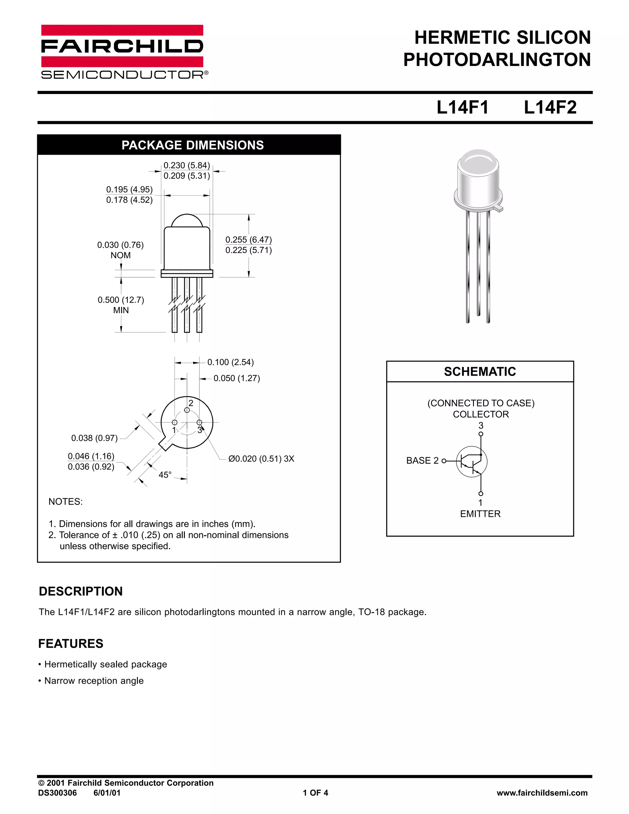
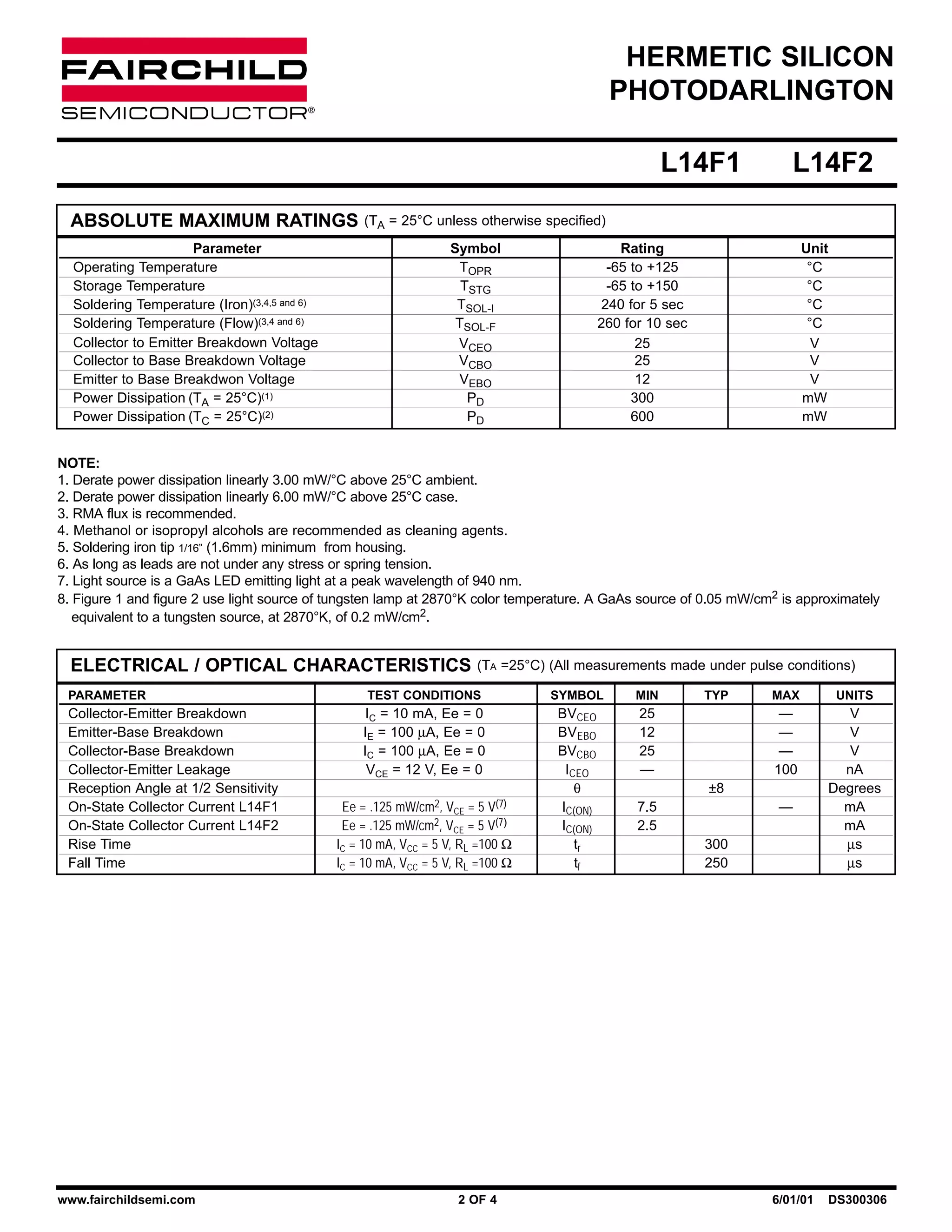
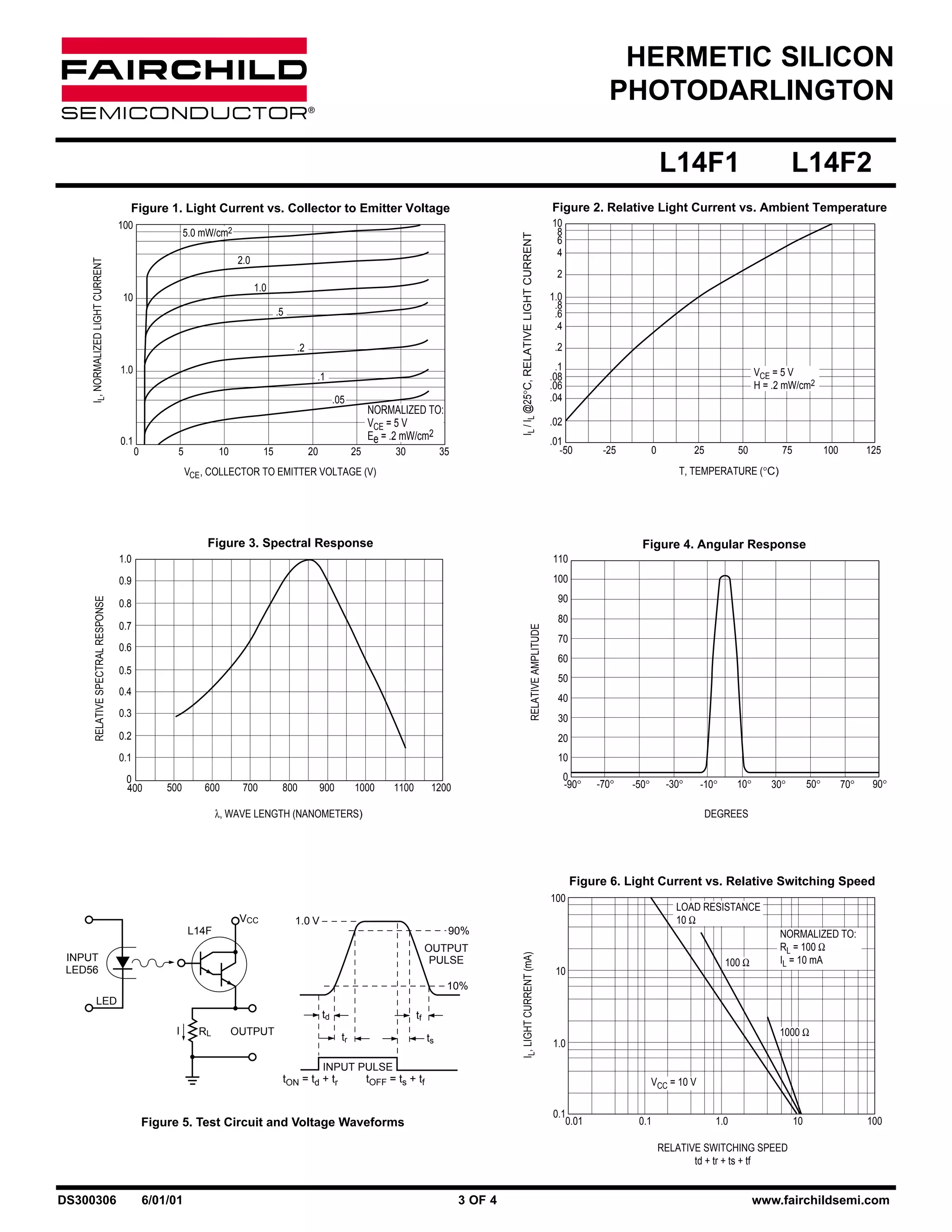

This document provides specifications for the L14F1 and L14F2 hermetic silicon photodarlingtons. It includes maximum ratings, electrical and optical characteristics, and test conditions. Key features are that they are hermetically sealed photodarlingtons packaged in a narrow angle TO-18 case. Graphs show characteristics such as light current vs voltage and temperature, spectral response, and angular response.


